Embed Size (px)
Citation preview

ACTAUNIVERSITATIS
UPSALIENSISUPPSALA
2017
Digital Comprehensive Summaries of Uppsala Dissertationsfrom the Faculty of Science and Technology 1519
On the Low Frequency Noise inIon Sensing
DA ZHANG
ISSN 1651-6214ISBN 978-91-554-9919-8urn:nbn:se:uu:diva-320544

Dissertation presented at Uppsala University to be publicly examined in Polhemssalen,Ångströmlaboratoriet, Lägerhyddsvägen 1, Uppsala, Friday, 9 June 2017 at 13:15 for thedegree of Doctor of Philosophy. The examination will be conducted in English. Facultyexaminer: Docent Michel Calame (Basel University).
AbstractZhang, D. 2017. On the Low Frequency Noise in Ion Sensing. Digital ComprehensiveSummaries of Uppsala Dissertations from the Faculty of Science and Technology 1519. 73 pp.Uppsala: Acta Universitatis Upsaliensis. ISBN 978-91-554-9919-8.
Ion sensing represents a grand research challenge. It finds a vast variety of applications in, e.g.,gas sensing for domestic gases and ion detection in electrolytes for chemical-biological-medicalmonitoring. Semiconductor genome sequencing exemplifies a revolutionary application of thelatter. For such sensing applications, the signal mostly spans in the low frequency regime.Therefore, low-frequency noise (LFN) present in the same frequency domain places a limit onthe minimum detectable variation of the sensing signal and constitutes a major research anddevelopment objective of ion sensing devices. This thesis focuses on understanding LFN in ionsensing based on both experimental and theoretical studies.
The thesis starts with demonstrating a novel device concept, i.e., ion-gated bipolar amplifier(IGBA), aiming at boosting the signal for mitigating the interference by external noise. AnIGBA device consists of a modified ion-sensitive field-effect transistors (ISFET) intimatelyintegrated with a bipolar junction transistor as the internal current amplifier with an achievedinternal amplification of 70. The efficacy of IGBA in suppressing the external interference isclearly demonstrated by comparing its noise performance to that of the ISFET counterpart.
Among the various noise sources of an ISFET, the solid/liquid interfacial noise is poorlystudied. A differential microelectrode cell is developed for characterizing this noise componentby employing potentiometry and electrochemical impedance spectroscopy. With the cell, themeasured noise of the TiN/electrolyte interface is found to be of thermal nature. The interfacialnoise is further found to be comparable or larger than that of the state-of-the-art MOSFETs.Therefore, its influence cannot be overlooked for design of future ion sensors.
To understand the solid/liquid interfacial noise, an electrochemical impedance model isdeveloped based on the dynamic site-binding reactions of surface hydrogen ions with surfaceOH groups. The model incorporates both thermodynamic and kinetic properties of the bindingreactions. By considering the distributed nature of the reaction energy barriers, the model caninterpret the interfacial impedance with a constant-phase-element behavior. Since the modeldirectly correlates the interfacial noise to the properties of the sensing surface, the dependenciesof noise on the reaction rate constants and binding site density are systematically investigated.
Keywords: low frequency noise, ion sensor, ISFET, electrochemical impedance spectroscopy,constant phase element, surface chemistry, CMOS technology
Da Zhang, Department of Engineering Sciences, Solid State Electronics, Box 534, UppsalaUniversity, SE-75121 Uppsala, Sweden.
© Da Zhang 2017
ISSN 1651-6214ISBN 978-91-554-9919-8urn:nbn:se:uu:diva-320544 (http://urn.kb.se/resolve?urn=urn:nbn:se:uu:diva-320544)

To my beloved wife


List of Papers
This thesis is based on the following papers, which are referred to in the text by their Roman numerals.
I Zhang, D. Gao X., Chen S., Norström H., Smith U., Solomon
P., Zhang S.L., Zhang Z. (2008) An ion-gated bipolar amplifier for ion sensing with enhanced signal and improved noise per-formance. Applied Physics Letters, 105(8):802102
II Zhang D., Must I., Netzer N.L., Xu X., Solomon P., Zhang S.L., Zhang Z. (2016) Direct assessment of solid-liquid interface noise in ion sensing using a differential method. Applied Phys-ics Letters, 108(15), 151603
III Zhang D., Solomon P., Zhang S.L., Zhang Z (2017) Low-frequency noise originating from the dynamic hydrogen ion re-activity at the solid/liquid interface of ion sensors. Sensors and Actuators B, submitted
IV Zhang D., Solomon P., Zhang S.L., Zhang Z (2017) Correlation of Low-Frequency Noise to the Dynamic Properties of the Sensing Surface in Electrolytes. ACS sensors, Submitted
Reprints were made with permission from the respective publishers.

Author’s Contributions
I Minor part of planning and the device fabrication, all of the TCAD simulation and measurement, and most of the data anal-ysis and the writing.
II Major part of planning, all of the device design and fabrication, EIS measurement and SEM, most of the data analysis, and all of the writing.
III Major part of planning, most of the model development, and all of the measurement, the data analysis and the writing.
IV All of the planning, most of the data analysis, and all of the writing.

Table of Contents
1. Introduction ............................................................................................... 13 1.1. Background ....................................................................................... 13
1.1.1. ISFET technology ...................................................................... 13 1.1.2. Noise sources in ISFET systems ................................................ 17
1.2. Research objectives ........................................................................... 18 1.3. Thesis organization ........................................................................... 19
2. Fundamentals ............................................................................................ 20 2.1. Sensing signal of ISFETs .................................................................. 20
2.1.1. Electrical double layer ............................................................... 20 2.1.2. Site-binding model and signal of ISFET ................................... 21
2.2. Thermal noise in ion-sensing systems ............................................... 23 2.2.1. Fluctuation-dissipation theorem ................................................ 23 2.2.2. Electrochemical impedance spectroscopy ................................. 23 2.2.3. Constant phase element and 1/f noise ........................................ 24
3. Enhance SNR via Internal Amplification ................................................. 27 3.1. Internal signal amplification .............................................................. 27 3.2. Integration of internal current amplifier ............................................ 29 3.3. DC Measurement of IGBA ................................................................ 31 3.4. SNR Enhancement via IGBA ............................................................ 32
3.4.1. Characterization details ............................................................. 32 3.4.2. Results and discussion ............................................................... 32
4. Assessment of Solid/Liquid Interface Noise in Ion-Sensing .................... 35 4.1. Differential microelectrode cell ......................................................... 35
4.1.1. Differential electrode configuration ........................................... 35 4.1.2. Fabrication of the differential microelectrode cell ..................... 36
4.2. Measurement methods ....................................................................... 37 4.2.1. Potentiometric noise .................................................................. 37 4.2.2. Thermal noise ............................................................................ 38
4.3. Result and discussion ........................................................................ 38 4.3.1. 1/f γ nature of oxide/electrolyte interfacial noise ....................... 38 4.3.2. Significant extrinsic noise in ISFETs ........................................ 40
5. Electrochemical Impedance Modelling for Solid/Liquid Interface........... 42 5.1. Model development ........................................................................... 42

5.1.1 Interfacial impedance based on site-binding reactions ............... 42 5.1.2 Variability in surface properties ................................................. 43
5.2. Application of the proposed impedance model ................................. 45 5.2.1 Experimental procedure and parameter extraction ..................... 45 5.2.2. K-distribution vs c-distribution .................................................. 46
6. Understanding Oxide/Electrolyte Interface Noise .................................... 49 6.1. Noise modeling analysis .................................................................... 49
6.1.1. Parameter extraction .................................................................. 49 6.1.2. Noise dependence on the site-binding admittance ..................... 50 6.1.3. Averaging of distributed interfacial properties .......................... 52
6.2. Correlation of LFN to surface dynamic properties ............................ 53 6.2.1. Effect of reaction rate constant .................................................. 53 6.2.2. Effect of site density .................................................................. 55 6.2.3. Summarized remarks ................................................................. 55
7. Concluding Remarks and Future Perspective ........................................... 57
Summary of the Appended Papers ................................................................ 59
Sammanfattning på svenska .......................................................................... 61
Acknowledgement ........................................................................................ 64
Reference ...................................................................................................... 66

Abbreviations and Symbols
ALD Atomic layer deposition BJT Bipolar junction transistor CE Counter electrode CMOS Complementary metal oxide semiconductor CPE Constant phase element EDL Electrical double layer EIS Electrochemical impedance spectroscopy dNTP Deoxynucleoside triphosphate EG Extended gate GCS Gouy-Chapman-Stern HGP Human genome project IGBA Ion-gated bipolar amplifier ISFET Ion-sensitive field-effect transistor J-N Johnson- Nyquist LDMOS Laterally diffused metal oxide semiconductor LFN Low-frequency noise LPCVD chemical vapor deposition MOSFET Metal oxide semiconductor field-effect transistor NGS Next-generation sequencing OCV Open-circuit voltage PCR Polymerase chain reaction PDMS polydimethylsiloxane PSD Power spectrum density PZC Point of zero charge RE Reference electrode RIE Reactive ion etching RMS Root-mean-square SEM Scanning electron microscope SBM Site-binding model SMU Source and measurement unit SNR Signal-to-noise ratio TEOS Tetraethyl orthosilicate WE Working electrode
Sa Surface hydrogen ion concentration buffC Buffer capacitance

DLC Electrical double layer capacitance diffC Diffuse layer capacitance SternC Electrical double layer capacitance
A B( )c c Reaction rate constant of protonation A0 B0( )c c A B( )c c at energy center
adAE ( ad
BE ) Activation energy for protonation reaction cE Distributed kinetic energy barrier KE Distributed Gibbs energy change
cf Corner frequency Mf Measurement frequency
A B( )G GΔ Δ Gibbs energy change mDg ( mCg ) Transconductance of ISFET(IGBA)
BI Base current CI Collector current DI Drain current EI Emitter current SI Source current
Di Internal current noise of ISFET ni Input current noise of readout circuitry
A B( )K K Equilibrium constant A0 B0( )K K A B( )K K at energy center SN Density of surface OH group SSN SN per unit energy
pHS Surface pH bR Liquid bulk resistance
A B( )r r Reaction rate constant of deprotonation HpS pH sensitivity
VS Noise PSD potVS Potentiometric noise PSD thVS Thermal noise PSD
inSNR Internal SNR exSNRα External SNR without internal amplification exSNRα External SNR with internal amplification
DV Drain voltage EV Emitter voltage GV Gate voltage TV Threshhold voltage nv Input voltage noise of readout circuitry SBY Site-binding admittance SBy SBY per unit energy CPEZ Impedance spectrum of a CPE intZ Solid/liquid interfacial impedance SBZ Site-binding impedance
β Current amplification of BJT

intβ Intrinsic buffer capacity +Θ Fraction of positively charged OH group
Θ− Fraction of negatively charged OH group 0Θ Fraction of neutral OH group 0σ Surface charge density ( )c Kσ σ Standard deviation of energy distribution
0ϕ Surface potential

12

13
1. Introduction
Noise is a stochastic process, appearing spontaneously as random time and/or space series of dynamic variables of interest [1]. Elimination of noise is impossible, because any substrate is subjected to thermal fluctuation, as long as the temperature is above 0 K. This thesis will look into this ubiqui-tous and everlasting phenomena present in ion-sensing applications. In Sec-tion 1.1, let’s use an example of ion-sensing applied in cutting edge technol-ogy to demonstrate the importance of addressing noise in the ion-sensing applications, which motivates the research objects of the thesis in Section 1.2 and thesis organization in Section 1.3.
1.1. Background 1.1.1. ISFET technology Human genome project (HGP) [2], genechips [3], personalized molecular diagnosis [4], etc., all such eye-catching concepts in life science and research are closely linked to a field – genome sequencing, the process of finding out the precise sequence of the four nucleotide base pairs in a DNA molecule. A DNA molecule comprises genes that bear the complete genetic information of a living organism. Therefore, accurate acquisition of the genetic infor-mation of the organism always has tremendous significance for the study of life science. The genome sequencing establishes a valuable method that guides people to find genes much more easily and quickly, which becomes an important progress towards understanding the complexity and diversity of lives.
Generally, the genome sequencing refers to any method or technology that can be used to determine the sequence of the bases. Based on the selec-tive incorporation of chain-terminating dideoxynucleotides by DNA poly-merase chain reaction (PCR) [5], [6], the Sanger sequencing method was developed in 1977 [5], prevailing approximately from the 1980s until the mid-2000s. However, the Sanger method is tremendously costly and time-inefficient. Initiated in 1990, the HGP based on the Sanger method con-sumed 2.7 billion dollars when it was declared complete in 2003 [7]. In the next decade, however, revolutionary technological advances reached the sequencing market [8]–[12], leading to much more efficient sequencing at

14
lower costs. The human genome can be sequenced within one day, at a cost of as low as around $ 1,000 in 2015 [13]. The emergence of fast and afford-able DNA sequencing is an important step towards personalized medicine, and revolutionized genomics and molecular biology.
Featured with high-throughput parallel sequencing, the set of the modern advanced sequencing technologies is collectively referred to as next-generation sequencing (NGS) [8], [9]. Among various cutting-edge ap-proaches, the ion-semiconductor, or Ion Torrent, sequencing technology [16] is one of the important players in the NGS arena, owing to its rapid and cost-effective test method[17], as well as its system-level integration using com-plementary metal oxide semiconductor (CMOS) technology. As shown in Figure 1(a), the Ion Torrent sequencing system is integrated as a bench-top platform, and its core component is a disposable sequencing chip, illustrated in Figure 1(b). On each sequencing chip, millions of microwells are fabri-cated, and each well contains a bead that bears over 10,000 replications of a single-stranded DNA template to be sequenced, as illustrated in Figure 1(c). During a sequencing process, the wells are sequentially flooded with A, C, G or T deoxynucleoside triphosphate (dNTP).[18]–[20] If the incoming dNTP is complementary to the next unpaired base on the DNA template, the dNTP molecule reacts with the nucleotide on each DNA strand to form a base pair, releasing a hydrogen ion (H+).
Figure 1. (a) Ion Torrent bench-top DNA sequencing platform, and its (b) Sequenc-ing chip. (c) The schematic cross-section of an ISFET fabricated on the sequencing chip as a pH sensor, by courtesy of J.M. Rothberg el.[16] On top of it is the liquid well where an acrylamide bead is placed to bear the DNA template.

15
Therefore, thousands of H+ released from the DNA replications decreases the local pH in the well, and the pH change is then detected by a metal-oxide-sensing gate beneath the well that is connected to the metal gate of a metal oxide field effect transistor (MOSFET), as marked in Figure 1(c). The MOSFET with an extended sensing gate is also called extended-gated ion sensitive field effect transistor (EG-ISFET)[21]–[23].
To understand the working principle of an ISFET, it is instructive to un-derstand the operation of its archetype configuration: a MOSFET. A typical MOSFET has three terminals, known as source, drain and gate, as depicted in Figure 2(a), i). The voltage VG applied to the gate can modulate the re-sistance between the source (S) and the drain (D), and hence the current ID flowing between them, provided that a certain voltage VDS is applied be-tween the source and drain. This ID - VG relation of an MOSFET, schemati-cally depicted in Figure 2(a), ii), is also known as transfer characteristics of the MOSFET. As seen in the figure, ID “turns on” as VG goes beyond a cer-tain knee point voltage denoted with VT. The corresponding theories have been extensively detailed in standard textbooks [24].
Figure 2. i) Cross-sectional sketches and ii) typical transfer characteristics of (a) a MOSFT and (b) an ISFET. The transfer characteristics are depicted with two distinct VT for the MOSFET, while with two pH values for the ISFET. At certain VRE, ΔID caused by changing pH for the ISFET is schematically depicted in iii) as well.
As to an ISEFT, a more general configuration than those with extended gates is illustrated in Figure 2(b), i), in which the solid metal gate of a MOSFET is replaced by a liquid under test. To operate the ISFET, a reference electrode

16
is submerged in the liquid and biased with VRE to anchor the electrochemical potential of the liquid. Therefore, ID - VRE relation represents the transfer characteristics of the ISFET. As pH of the liquid varies, to maintain surface equilibrium, amphoteric hydroxyl (OH) groups on the oxide surface can capture/release H+, accordingly, resulting in surface charge variation. Thus, the oxide surface electric potential φ0 with respect to the liquid bulk will change, modulating the resistance between S and D and then causing a change in ID. Therefore, the transfer curve shifts as the pH value changes, as illustrated in Figure 2(b), ii). ΔID caused by ΔpH at a certain VRE is referred to as the signal of the ISFET. The quantification of φ0 – pH relation becomes a crucial concern for understanding the operation principle of an ISFET, which has been well addressed by the site-binding model (SBM) and will be briefly discussed in next section.
The ISFET applied in Ion Torrent technology is fabricated with the stand-ard CMOS technology, granting it another significant advantage: the ability to scale with Moore’s Law. Moore's law, based on the observed trend over the past decades, states that roughly every two years the amount of transis-tors in a single integrated circuit chip doubles, leading to more high-performance chips with denser packages. It means that the throughput of the Ion Torrent sequencing system can be brought even higher, with a denser ISFET array, which is readily achieved by scaling down the ISFET’s sizes via the CMOS technology [25].
However, ultra-scale integration of ISFET is not always beneficial, in terms of the noise performance of the ISFET. As Figure 3[16] shows, nota-ble fluctuation appears at the signal baseline (0 count), as the diameter of the liquid well on top of the ISFET decreases, which may be caused by various mechanisms, such as the higher potential noise with smaller sensing gate area, and boosted cross-talk from the denser integration, etc.
Figure 3. Sequencing signal (measured in the voltage counts) v.s. base flow for the Ion Torrent sequencer from (a) 3.5 µm diameter well and (b) 1.3 µm well of its ISFETs, by courtesy of J.M. Rothberg el.[16] Note the larger fluctuation at the signal base for the smaller size.
Since complete elimination of the noise is impossible, in any sensing system, the noise will ultimately determine the sensing resolution, by placing a limit on the minimum detectable variation of signal. For sensing applications like
17
Ion Torrent sequencing, a single base incorporation leads to a 0.02 pH varia-tion [16], corresponding to around 1 mV change in the surface potential pro-vided the Nernst response applies. To measure such a small potential change, the noise in the sensing system must be mitigated to an appreciable extend.
1.1.2. Noise sources in ISFET systems The major contribution to the noise in ion-sensing applications dominates in the low-frequency regime, where sensing experiments are typically per-formed [26]. Besides, heavy metallization in sensing chips is subject to low frequency noise coupling which can interfere with biomedical signals that mostly span in the same frequency domain [27]. Hence, low-frequency noise (LFN) becomes an significant performance-limiting factor for ion-/bio-sensitive FET systems, which has thus received extensive in-depth investiga-tions [26], [28]–[46]. The noise sources of an ISFET system are sorted out as follows.
In an ISFET-based ion sensing system, any noise sources outside the ISFET itself are referred to as the external noise, such as environmental in-terference and instrument noise from terminal read-out circuits [47] etc., as illustrated in Figure 4. It can be demanding or even impossible to mitigate the external noise, but their interference can be diminished by internally amplifying the signals, as will be discussed in next chapter,
Figure 4. Noise sources appearing in an ion sensing system consisting of an ISFET and characterization instrument. The noise associated with the solid/liquid interfacial interaction is a research focus of this thesis.
Noise present inside an ISFET is referred to as the internal noise of the ISFET, falling into intrinsic and extrinsic parts, which is also illustrated in Figure 4. The intrinsic noise refers to that appearing in the solid part of an ISFET. It consists of, among other possible sources, the channel noise [28], [30]–[32], [36], [38], [41], [43] caused by fluctuation of the carrier number (ΔN) and/or mobility (Δµ), the thermal noise associated with the dielectric

18
absorption [40], [42], the shot noise arising from the electrical potential bar-rier [48], and thermal noise associated with the contact resistance of the source and drain terminals [33]. On the other hand, the noise of an ISFET can also originate from the liquid part of the ISFET, referred to as extrinsic noise of the ISFET. The extrinsic noise is generally rooted in ionic interac-tion at the liquid/oxide interface [26], [37], [39], [44], [46], electrochemical process between liquid and RE [29], as well as thermal noise from the liquid bulk.
The theoretical and experimental concerns behind the intrinsic noise sources have been well understood in the literatures. The extrinsic noise originates from the RE and liquid bulk can be accounted for by well-established models [29], owing to the simplicity of the associated electro-chemical process. The major challenge of addressing the noise of the ISFET lies in understanding the solid/liquid interfacial noise.
1.2. Research objectives This thesis work aims at a systematic investigation of the LFN present in the field-effect ion sensing systems, and, in particular, understanding the noise originating from the solid/liquid interface where the signal to be detected is generated and the corresponding sensing mechanisms are sought for. First, to diminish the external interference, technology of the internal amplification needs to be explored. Second, one major challenge is to accurately assess the solid/liquid interfacial noise, which motivates a dedicated characterization tool. Last, understanding the noise significantly relies on a theoretical model that incorporates the physical properties of the solid/liquid interface, in order to establish the relationship between the noise and such properties.
In terms of the above experimental and theoretical concerns, the tasks of the thesis are summarized as • to design and fabricate the dedicated device for internal amplification. • to design and fabricate the dedicated device for the solid/liquid interfa-
cial noise study, • to develop a theoretical model that links the interfacial noise to the phys-
ical properties of the interface, and • to utilize the model to interpret the noise behavior, as well as its depend-
ence on the interface properties.

19
1.3. Thesis organization The thesis is structured as follows:
Chapter 2 introduces the electrical double layer (EDL) structure as well as SBM for explaining the pH-sensing principle of the ISFET, as well as the theoretical background of the thermal noise present in ion-sensing.
Chapter 3 demonstrates the novel device concept towards signal-to-noise ratio (SNR) enhancement for the ISFET systems by suppressing the interfer-ence from the external noise. The conceptualized internal amplification, as the operation principles of the device, is described. The CMOS technology-based fabrication flow for the device is detailed as well. The DC and noise spectrum characterizations of the device are shown to indicate its efficacy of achieving greater SNR.
Chapter 4 introduces a differential microelectrode array dedicated for characterizing the solid/liquid interfacial noise. The working principle of the differential measurement and the fabrication details are described. The noise measurement setups based on potentiometry and electrochemical impedance spectroscopy for the electrode cell are described, and the measurement re-sults are summarized and discussed.
In Chapter 5, an electrochemical impedance model, based on the hydro-gen ion reactivity at the oxide/electrolyte interface, is developed for studying the physical mechanism behind the interfacial noise. The modeling method is detailed, and the validity of the model is justified through the extracted modeling parameters.
In Chapter 6, the proposed impedance model is explored in detail, in or-der to find out the dependence of the interfacial noise on the surface dynamic properties.
The thesis is concluded in Chapter 7 with a general summary and a future outlook. In Chapter 8 an overview of the appended papers is provided.

20
2. Fundamentals
Noise can be rooted in variety of mechanisms. From the standpoint of elec-tronic ion sensing, the noise refers to the unwanted fluctuation superimposed on an electrical signal. In this chapter, the fundamentals pertaining to the noise present in electronic sensing systems, particularly ISFET, are briefly reviewed. In section 2.1, the structure of electric double layer (EDL) as well as site-binding model (SBM) will be discussed firstly, in order to quantify the ISFET signal. Then, the basics and characterization of thermal noise will be discussed in section 2.2.
2.1. Sensing signal of ISFETs 2.1.1. Electrical double layer
Figure 5. Schematic of an EDL at the interface between a negatively charged oxide and and electrolyte. The distribution of electrical potential φ from the oxide surface to the liquid bulk is also illustrated.
When a solid electrode is brought in contact with a liquid, two spatially sep-arated charge layers from the liquid will appear on top of the electrode sur-

21
face, referred to as EDL. The EDL structure plays a fundamental role in the surface charging. Therefore, understanding the EDL structure at the ox-ide/electrolyte interface is import for understanding the corresponding charg-ing mechanism. Many EDL models have been applied successfully in their respective regard, in which the Gouy-Chapman-Stern (GCS) model has been extensively employed for ISFET applications [49]. In Figure 5, the EDL structure described with the GCS model is schematically depicted for a nega-tively-charged oxide in contact with an electrolyte. As shown in the figure, the first layer of the EDL, i.e. the Stern layer, consists of the solvated ions adsorbed onto the oxide surface due to chemical interactions [50]. The sec-ond layer, i.e. the diffuse layer, comprises the ions attracted electrostatically by the surface charge, loosely surrounding the oxide surface [50]. Then, the surface potential φ0 is the potential drop across both layers, and the EDL capacitance CDL is the series connection of the Stern capacitance CStern and the diffuse layer capacitance Cdiff, as expressed with the following relation:
1 1 1DL Stern diffC C C− − −= + (2.1)
2.1.2. Site-binding model and signal of ISFET The well-known Nernstian equation predicts that the variation of Sϕ with one pH unit change of solution, also known as pH sensitivity, is 59.2 mV at room temperature. In the case of oxide/liquid systems, however, the ob-served pH sensitivity is generally less than 59 mV. To explain the deviation, the site-binding model [51], as well as its derivatives[52], [53], was devel-oped to describe the charging for an oxide/liquid interface, which successful-ly interprets the observed non-Nernstian sensitivity and has been widely accepted as the primary charging mechanism of the oxide-liquid interfaces. In the context of SBM, the oxide charging is ascribed to the H+ adsorption to/desorption from the amphoteric OH group, i.e. protonation/deprotonation, on the oxide surface, as summarized by the following reversible reactions:
M–OH↔M–O + H (2.2a)
M–OH ↔M–OH + H (2.2b)
where, SH+ denotes the surface H+. In thermal equilibrium, the two reactions are equilibrated by the following detailed balances:
A S A[M-O ] [M-OH]c a r− = (2.3a)
B S B 2[M-OH] [M-OH ]c a r += (2.3b)

22
where, [M-O ]− , 2[M-OH ]+ , and [M-OH] denote the density of deprotonat-ed, protonated, and uncharged surface OH groups, respectively, and aS the
SH+ concentration; c and r represent the reaction rate constant for the H+ adsorption and desorption, with subscripts A and B referring them to reac-tions (2.2a) and (2.2b), respectively. By definition, cA and cB are related to the kinetic barriers of the H+ adsorption ad
AE and adBE via:
ad adA B
A A Bexp , expB
E Ec c c c
kT kT
′ ′= − = −
(2.4)
where Ac′ and Bc′ are constants, k is the Boltzmann constant, T the tempera-ture. Likewise, rA and rB are functions of the kinetic energy of the H+ desorp-tion, with the same form as cA and cB. Therefore, the surface equilibria can be characterized by two thermodynamic equilibrium constants as follows:
A A B BA A B B
A B
exp , expr G r G
K K K Kc kT c kT
Δ Δ ′ ′= = − = = −
(2.5)
in which, AK ′ and BK ′ are constants, and the two ΔG:s denote the Gibbs free energy changes for reactions (2.2a) and (2.2b), respectively. In practice, KA and KB are often featured with their logarithmic potential, i.e.
A 10 AK log ( )p K= − and B 10 BK log ( )p K= − . The surface charging condi-tion, and thus 0ϕ , at a certain pH can be solved with the known values of KA and KB, which, however, is a clumsy process with the classic site-binding model [52].
To overcome the complexity of the classic SBM, van Hal el. developed a general approach [53] to calculate the pH sensitivity. In their approach, the surface H+ buffer capacity, intβ , was introduced, to quantify the capability of an oxide surface to buffer the variation of the SH+ concentration, so that a concise but physically meaningful expression for the pH sensitivity, HpS , was found as follow:
0H
D L2
int
59 .2 m V / H2.3H 1
p
pS
kTCpq
ϕ
β
ΔΔ
= =+
(2.6)
where, q is the elementary charge. The calculation of intβ and CDL depend on the charging mechanism and the EDL model to be applied, respectively. For the aforementioned SBM, intβ can be expressed as [53]:
0 2 B Sint S 2
S 1
d12.3
d H
D K aN
q p D
σβ = = (2.7)

23
where 0σ denotes the surface charge density, NS the density of surface OH group, and 2
1 A B B S SD K K K a a= + + and 21 A B A S S4D K K K a a= + + . On the
other hand, CDL can be calculated via the GCS model [50]. Hence, the 0 Hpϕ − relation, featured with HpS in Eq (2.6), can be accurately deter-
mined, given that intβ and CDL are evaluated via Eqs. (2.6) and (2.7). For the detailed calculation procedure the reader is referred to the cited literature. The signal of an ISFET, i.e. the change of ID caused by that of pH, can then be quantified, in accordance to the known transfer characteristic and HpS of the ISFET.
2.2. Thermal noise in ion-sensing systems 2.2.1. Fluctuation-dissipation theorem Thermal noise, also known as Johnson- Nyquist (J-N) noise, is caused by the random motion of charge carriers agitated thermally in an electrical conduc-tor. It was detected by J. B. Johnson [54], and then was interpreted by H, Nyquist [55], with the thermally-agitated electromotive force in conductors. This noise is present in any substances that include charge carriers beyond T=0 K. Particularly in ion-sensing systems where liquid is involved, the elec-trons and holes in the solid electrodes and the ions in the liquid are all sub-jected to the thermal agitation, and thus generate the J-N noise. Its power spectral density (PSD) in terms of electrical potential is proportional to the real part of the electrical impedance spectrum Z( f ) of the systems under test, which is expressed as [55]:
V ( ) 4 Re[ ( )]S f kT Z f= (2.8)
where, f denotes frequency. Eq. (2.8) insightfully reveals the physical nature of the thermal noise of the charge carriers, generalized with the fluctuation-dissipation theorem [56]: the process in which the thermal agitation causes the random fluctuation of the carriers is equal to its reversed process where the kinetic energy of the moving carriers is transferred into heat throughRe[ ( )]Z f .
2.2.2. Electrochemical impedance spectroscopy Eq. (2.8) is significant, not only because it provides fundamental understand-ing for the thermal noise, but the equation also points out that the thermal noise of a system can be probed by measuring its impedance spectrum. For ion-sensing systems in particular, the characterization of ( )Z f refers to electrochemical impedance spectroscopy (EIS) [57], which usually employs a three-electrode measurement setup consisting of a working electrode

24
(WE), a counter electrode (CE) and a reference electrode (RE), as schemati-cally shown in Figure 6. The WE is the electrode where electrochemical processes of interest are present; the CE is used to balance the current pass-ing through the WE; the RE, with a known fixed electrode potential, acts as reference point for measuring and gauging the WE potential, ideally with no current flowing through it.
Figure 6. Three-electrode setup for EIS characterization. WE, RE and CE represent working, reference and counter electrode, respectively.
To perform an EIS measurement, a desired DC potential of the WE is firstly biased with respect to the RE, by applying a potential between the WE and CE. Then, an AC voltage at a certain frequency is applied on the WE with respect to the RE as well, and the responding AC current is recorded concur-rently by an ammeter in the same current loop. Finally, ( )Z f is obtained by dividing the AC voltage with the responding AC current at various sampling frequencies. All the controlling and measuring electronics, as well as data acquisition and analyzer, can be integrated as a compact instrument known as a potentiostat.
2.2.3. Constant phase element and 1/f noise For purely resistive components such as metal leads, semiconductor and liquid bulk, Re[ ( )]Z f in Eq. (2.8) is reduced to a resistor, making VS inde-pendent of f at a certain temperature, also known as white noise. However, more complicated impedance behaviors can appear locally, such as at sol-id/liquid interfaces, where Re[ ( )]Z f can be dependent on frequency and becomes significant under low frequencies.
The impedance for a charge-transferring Faradaic interface is expected to be a semicircle in a Nyquist diagram, centered on the x-axis, which can be represented by a simple equivalent circuit model consisting of a resistor R connected in parallel with a capacitor C [58]. However, the Nyquist plot of

25
the experimentally measured impedance data usually becomes a semicircle rotated around its high-frequency endpoint (left end), with its center lying below the x-axis [58]–[60], as illustrated in Figure 7(a). On the other hand, for blocking non-Faradaic systems such as insulating oxide/liquid interfaces, the electrochemical impedance in a Nyquist diagram often exhibits a straight line rotated around the high-frequency endpoint (lower end), with a phase angle smaller than 90°, instead of a vertical line represented by a pure C [59], as illustrated in Figure 7(b).
Figure 7. Typical impedance spectrum with CPE behaviors plotted in Nyquist dia-grams for (a) Faradaic and (b) non-Faradaic systems, respectively.
These impedance behaviors cannot be accounted for by any simple R-C net-work, and are often represented by an phenomenological circuit component referred to as the constant phase element (CPE) [57], [61], with the imped-ance spectrum expressed as CPE ( ) 1 ( )Z f Q if γ= , where i is the imaginary unit, Q a CPE parameter and γ ranges from 0 to 1 in an electrochemical sys-tem [60]. Therefore, VS of the thermal noise featured with the CPE behavior can be found as:
V CPE
cos( 2) 1( ) 4 Re( )
(2 )S f kT Z
Q fγ γπγπ
= = (2.9)
Note that V ( ) 1S f f γ∝ , and hence the J-N noise featured with the CPE behavior can be appreciably large as the frequency decreases. The noise with PSD subjected to this form is generally called 1/f noise. In the context of electrochemical systems, the physical interpretation of the CPE behavior is still under debate, although it is generally accepted [61], [62] either to root in spatial structural heterogeneities of electrodes [63]–[69] or to arise from varying time constants associated with different physical processes distribut-ed at the electrode surface [70]–[76].

26
It should be noted that the 1/f noise appears in more than the liquid-involved systems. Some noise in the solid phases of the ion-sensing systems is also of the 1/f form, such as the channel fluctuation as discussed in Chap-ter 1. The latter, however, has been well addressed in the literature, and is beyond the scope of this thesis.

27
3. Enhance SNR via Internal Amplification
As discussed in Chapter 2, an ISFET system is inevitably faced with the interference from external noise. In terms of measurement practice, amplify-ing the internal signal without bringing in extra noise is an intuitive way to suppress the external interference, and thus improve SNR for the ISFET systems. This can be achieved by the new device concept demonstrated in this chapter. First, section 3.1 will discuss how the SNR is boosted via am-plifying the internal signals, and then bipolar junction transistors (BJTs) will be introduced for the internal current amplification. The fabrication details of the designed amplifier will be described in section 3.2. Last, the DC perfor-mance of the fabricated device will be discussed in section 3.3, and noise performance benefiting from the device will be analyzed and discussed in section 3.4.
3.1. Internal signal amplification Since signal current of an ISFET, ∆ , is relatively small, an external readout circuitry is commonly used to amplify the signal, as depicted in Figure 8.
Figure 8. Schematic representation of an ISFET measurement system with an exter-nal readout. The red dashed line represents the signal flow with internal amplifica-tion. The external SNR with ( exSNRα ) and without ( exSNRβ ) internal amplification (β) are formulated, indicating SNR is boosted with the internal amplification.

28
Both ∆ and the internal current noise of the ISFET are amplified simul-taneously. However, extra input current and voltage noise associated with the external readout circuitry, represented with and in Figure 8, is am-plified and thus contributes to the total noise as well, making the external SNR ( exSNRα ), as formulated in the figure, inferior to the internal one (SNRin).
In terms of the measurement practice, if the internal current of the ISFET, i.e. ∆ + , can be amplified before the external readout stage, without introducing extra noise, the external SNR will be altered to exSNRβ , as for-mulated in Figure 8. As long as β is large enough, the internal items, ∆ and , in the exSNRβ expression will dominate compared to the external noise, which leads to ex exSNR SNRβ α> . This means the SNR in practice is improved by the internal amplification.
To avoid introducing additional noise, the internal amplifier should not introduce extra noise, and be placed as close to the output terminal of ISFET as possible. This can be achieved by a BJT which can be integrated with the ISFET tightly using standard CMOS technology. BJTs have two doping configurations, pnp and npn. Taking pnp type as an example, the BJT has two back-to-back PN junctions, forming three doped regions with different charge concentrations and polarities, as illustrated in Figure 9. The three regions of the BJT are p-doped emitter (E), n-doped base (B) and p-doped collector (C), respectively. The E region is heavily doped, while the doping levels of the other two are similar.
Figure 9. n-channel ISFET with drain connected to the base of a pnp BJT as the current amplifier. The typical log(I)-VE plot of a BJT shows current amplification.

29
To operate the BJT, the E-B junction is forward biased, whereas the B-C junction is reverse biased, which can be performed by biasing a positive voltage between terminals E and C, as illustrated in Figure 9. Under the forward bias, many holes (h+) in heavily doped E region are injected into lightly doped B region, whereas few electrons (e-) diffuse back from B to E. On the other hand, minority of h+ coming from the E region recombine with e- in B region, while majority of them diffuse through the base and then be swept into the C region by the strong electric field between B and C caused by the reverse biased B-C junction. In terms of current through each termi-nal, the collector current IC, almost identical to the emitter current IE, is greater than the base current IB, with a certain amplification ratio β= IC/ IB, as illustrated in Figure 9.
3.2. Integration of internal current amplifier The tight integration of the BJT to the ISFET was facilitated by designing
a novel device, ion-gated bipolar amplifier (IGBA). The cross-sectional rep-resentation of the IGBA device is schematically shown in Figure 10. In the design, a laterally-diffused metal-oxide-semiconductor field-effect transistor (LDMOS-FET), acting as the modified ISFET, is laterally connected to the base of a vertical BJT. This way, the drain current, ID, of the ISFET is im-mediately amplified by the BJT and leaves the device as a significantly en-hanced collector current, IC. As used in Ion Torrent technology and many other ion-sensing applications [77]–[80], an extended gate (EG) setup was employed for pH sensing demonstration. The EG structure in our setup is also schematically depicted in Figure 10, where, 1-µm-thick aluminum is
Figure 10. Schematic cross section of the IGBA device, as well as the EG-based pH measurement setup.
sputtered on a glass sheet, followed with the deposition of a 100-nm atomic-layer-deposited Al2O3 layer as the pH sensing material. A polydime-

30
thylsiloxane (PDMS) liquid container is glued on the EG, with a Ag/AgCl RE immersed in the solution to bias it.
Figure 11. Simulated doping profile for (a) the whole IGBA device and (b) the zoom-in on the LDMOS-FET.
The IGBA device was fabricated via the standard silicon technology, and the simulated doping profile is shown in Figure 11(a). The substrate is a Boron-doped (5×1018 cm-3) p+ (100)-bulk wafer with a 6.5-µm-thick Boron-doped (1×1015 cm-3) epitaxial layer. The p+ substrate serves as the C region of the BJT, being accessed with a p-ring plugged-in around the active area. The n region, formed by compensated Phosphorus implantation and thermal drive-in, acts not only as the base of the vertical pnp BJT but also the drain of the n-channel LDMOS-FET. 25-nm-thick SiO2, as labeled in Figure 11(b), was then grown by thermal oxidation, above which the poly-silicon gate stack was formed via low-pressure chemical vapor deposition (LPCVD) and reac-tive ion etching (RIE). The p-well was formed by B+ implantation, followed by a thermal annealing aiming not only to activate the dopants, but also to form a laterally diffused p-region under the gate stack as the n-
Figure 12. (a) Layout of contacting pads in photo lithography mask for the IGBA device. (b) Top-view of the central part of the fabricated device by SEM.
channel of the LDMOS-FET, as noted in Figure 11(b). The four heavily doped regions are the electrical accesses to the n-drain (D), the p-substrate

31
and the n+ source (S) of the LDMOS FET, and the p+ E region of the BJT, respectively. 400-nm-thick tetraethyl orthosilicate (TEOS) was, then, coated as a preliminary passivation. Consequentially, other than terminals E and C of the BJT, the IGBA has another two terminals, source S and gate G, as depicted in the Figure 10. At the end of the fabrication flow, a layer of Alu-minum was sputter-deposited, followed by RIE to form the contacting pads for all the terminals. The contacting pad layout of the designed device in the photo lithography mask is shown in Figure 12(a), and the top-view of the fabricated device via scanning electron microscopy (SEM) is shown in Fig-ure 12(b).
3.3. DC Measurement of IGBA
The DC transfer characteristics, as well as the current amplification of the IGBA were characterized using an HP4155 precision semiconductor analyz-er, as illustrated in Figure 13(a). During all the measurements, terminals S and C were biased at 0 V via two source measurement units (SMUs) of the HP4155 with respective to the common ground of the analyzer. For charac-terizing the transfer characteristics, the E terminal was biased with another
Figure 13. (a) IC-VG transfer and gmC characteristics of the IGBA compared to ID-VG and gmD of its reference ISFET and (b) IC-t measurement for pH sensing with the IGBA compared to ID-t of its reference ISFET, as well as the respective measure-ment setup. Note that ID is equal to the measured IS.

32
SMU at a certain potential VE=0.75 V above the built-in potential (about 0.6 V at room temperature) of the p+-n emitter-base junction to turn on the ver-tical BJT, and thus the whole device. Since IS is almost equal to ID of the ISFET, the measured value of IS is regarded as ID of the ISFET. ID and IC of the BJT were recorded simultaneously by the corresponding SMUs at vary-ing VG, and they, as functions of VG, are depicted in Figure 13(a), in which the corresponding transconductances gmD and gmC, defined as gmD=dID/dVG and gmC=dIC/dVG , are also shown. The threshold voltage, VT, is indicted in the figure with vertical broken lines. As seen, the current gain of the IGBA over the ISFET itself, i.e., IC/ID, is 60–80 in both weak inversion (subthresh-old) (below VT) and moderate inversion (above VT) regions
For demonstrating pH measurement in electrolytes, the Al2O3/Al EG was bonded to terminal G, as illustration in Figure 13(b). The RE was then bi-ased at a constant potential VRE=1.5 V, and the variations of ID and IC with time, t, at different pH values in solution were monitored, as depicted in Figure 13(b). The pH values in the figure are nominal. They were altered manually by the titration of hydrogen chloride (HCl) into the solution. The results in the figure clearly demonstrate significant signal amplification of the IGBA in pH sensing applications
3.4. SNR Enhancement via IGBA 3.4.1. Characterization details For the LFN characterization, the IGBA and its internal ISFET were ana-lyzed separately. In both measurements, VG was identical and so was VS (grounded). IC of the IGBA, as a function of time, was monitored at a cer-tain VE while VC was grounded. The variation of ID of the ISFET with the time was accessed via an additional contact to its drain terminal with a bias VD (not shown in Fig. 1) while leaving terminals C and E unconnected. In order to make a fair comparison, VD for the ISFET was set to render ID iden-tical to IS of the IGBA. The biases in the terminals were applied using bat-teries. The fluctuation in ID and IC was first amplified by a TI TL071 low- noise preamplifier and then monitored at a sampling rate of 1000 Hz for 20 seconds using an Agilent B1530A Waveform Generator/Fast Measurement Unit. The current noise spectrum was analyzed using the signal processing toolbox in Matlab.
3.4.2. Results and discussion The noise on ID is inevitably amplified by the internal BJT. To quantify the noise and SNR, the PSD of the current noise as a function of f, was first characterized for IC of the IGBA, denoted as , and ID of the internal

33
ISFET, as . The VG-referred PSD of voltage noise, SV, was then ob-tained by employing the following relationship:
IGBA ISFET
IGBA ISFETI IV V2 2
mD mC
, S S
S Sg g
= = (3.2)
The resultant and measured at VE=0.75 V, with VG biased at 0.25, 0.3 and 0.38 V are depicted in Figure 14(a), (b) and (c), which corre-spond to the subthreshold, weak inversion and strong inversion regimes, respectively. The dashed lines show the thermal noise of the ISFET under the same bias conditions for the corresponding case, calculated via =2 3⁄ × 4 ⁄ . Two important observations can be found. First, the curve is almost 10 times lower than the ones in the entire measure-ment range from f=1 Hz to f=500 Hz. Second, the large spikes at 50 Hz and its higher harmonics in the ISFET are completely suppressed in the IGBA since they are smaller than the amplified signal.
Figure 14. The measured SV-f characteristics for the IGBA and its ISFET counter-part, at VE=0.75 V and (a) VG=0.25 V, (b) VG=0.30 V and (c) VG=0.38 V with the dashed line showing the corresponding calculated thermal noise of the ISFET under the same bias conditions. (d) Gain_SNR at different VG for two frequency integra-tion intervals in (a).

34
This much desired advantage with improved noise performance of the IGBA primarily results from signal amplification before it becomes contaminated by external interferences including noise generated by the low-noise pream-plifier in the characterization system. As expected, the difference between
and diminishes when VG is increased above VT at which both IC and ID increase by more than 100 times and the sensors themselves become noisier. Hence, the gain in SNR for the IGBA with referenced to the ISFET, which is calculated as:
ISFET2 2VmC mD
IGBA ISFET IGBAI I V
dGain_SNR=
d d d
S fg g
S f S f S f=
(3.3)
asymptotically approaches unity with increasing VG, cf. Figure 14(b). The remaining SNR-benefit for the IGBA at VG≥VT is simply a consequence of the effective suppression of the spikes associated with 50 Hz and its harmon-ics. The effect of the spikes on Gain_SNR is better elucidated by including them in the SI integral from f=1 Hz to f=500 Hz; Gain_SNR is found to in-crease from 2-3 when the integration spans from f=1 Hz to f=50 Hz to around 6 when the integration range extends to f=500 Hz.

35
4. Assessment of Solid/Liquid Interface Noise in Ion-Sensing
In terms of the measurement practice, the noise performance for ion-sensing applications can be enhanced externally with the novel device concept, as detailed in Chapter 3. The internal SNR in ion sensing, however, cannot benefit from the same technology. On the other hand, reliable characteriza-tion tools for extracting the detailed information associated with the internal noise in ion sensing should always be the very first step on the way towards understanding the noise and even improving noise performance. Developing the tool will be the focus of the chapter. Section 4.1 will deal with the design and fabrication of the electrode cell dedicated for LFN characterization of an electrochemical system. Based on the electrode cell, related characterization techniques used will be detailed in section 4.2. At last, in section 4.3, the result of the noise measurement will be analyzed and discussed.
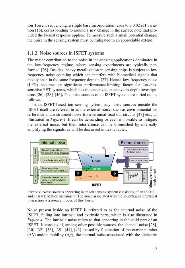
4.1. Differential microelectrode cell 4.1.1. Differential electrode configuration As discussed in chapter 2, the noise characterization for the ISFETs is spe-cialized on investigating the noise originating from the solid/liquid interfac-es, which can be fulfilled with the differential electrode configuration, as will be introduced immediately.
Bearing native oxide that has a pH sensitivity close to the ideal Nernstian response with 59 mV/pH at room temperature [81], electrically conductive titanium nitride (TiN) was chosen as prototype sensing material of the elec-trode cell, in order to demostsrate its working principle. As schematically shown in Figure 15, the electrode cell was designed to have two identical TiN electrodes, in order to facilitate a direct assessment of the voltage noise via differential measurements. In the differential measurement, equal amount of DC potentials across the EDL build up at the two identical TiN|TiOx|liquid intefaces, at a given pH value. As sensing surfaces are face-to-face in the measurement loop, their DC components ( ) would cancel out with each other. In contrast, two identical AC voltage noise sources, denoted as would be in series and independent of each other, as indicated in the schematics. Note that as long as the liquid concentration is high
36
Figure 15. Schematic diagram of the differential microelectrode cell, in which represents the DC potential across the EDLs, and denotes the AC voltage noise sources.
enough so that the associated J-N noise is trivial, the total measured noise power would, then, be a summation of the contributions from the bulk elec-trolyte and the two EDLs.
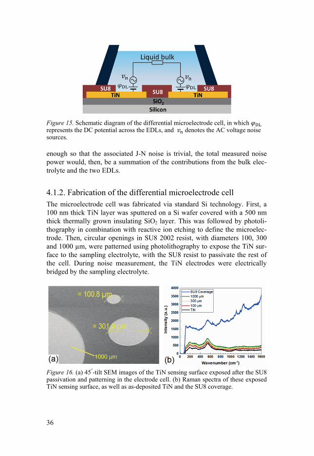
4.1.2. Fabrication of the differential microelectrode cell The microelectrode cell was fabricated via standard Si technology. First, a 100 nm thick TiN layer was sputtered on a Si wafer covered with a 500 nm thick thermally grown insulating SiO2 layer. This was followed by photoli-thography in combination with reactive ion etching to define the microelec-trode. Then, circular openings in SU8 2002 resist, with diameters 100, 300 and 1000 µm, were patterned using photolithography to expose the TiN sur-face to the sampling electrolyte, with the SU8 resist to passivate the rest of the cell. During noise measurement, the TiN electrodes were electrically bridged by the sampling electrolyte.
Figure 16. (a) 45°-tilt SEM images of the TiN sensing surface exposed after the SU8 passivation and patterning in the electrode cell. (b) Raman spectra of these exposed TiN sensing surface, as well as as-deposited TiN and the SU8 coverage.

37
The SU8 openings, inspected by SEM as presented in Figure 16(a), were confined within the patterned TiN area, thereby ensuring exposure of only the TiN surface to the electrolyte. The surfaces of the TiN electrodes were free from SU8 contamination within the detection limit of Raman spectros-copy, as shown in Figure 16(b).
4.2. Measurement methods 4.2.1. Potentiometric noise The potentiometric measurement setup is schematically shown in Figure 17. The measurement loop comprises the two TiN electrodes and a KCl (Merck) aqueous solution as the sampling electrolyte, because KCl electrolyte is widely applied in (bio-) chemical sensing. The KCl concentration was varied from 1 mM to 1 M at two pH values 6 and 2. To measure the voltage noise, a preamplifier with a 0.1 Hz – 1 kHz bandpass filter and a gain of 10k was constructed using OPA140 operational amplifiers, and the signal was digit-ized using a Keysight U2351a multifunction data acquisition device. The electrical potential variation between the two electrodes was sampled at 10 kHz and 4 million data points were used to generate its voltage PSD, . The noise PSD was divided by 2 so as to normalize it to a single electrode.
Figure 17. Schematic noise measurement setups for the TiN/KCl system with the differential microelectrode cell, via potentiometry specified in section 4.2.1 and EIS in section 4.2.2. It should be noted that the two measurement systems should work alternatively, which means only one of them is connected to the cell at a time.

38
4.2.2. Thermal noise A comparison between the potentiometric and thermal noise give rise to insightful understandings of the interfacial noise. Thus, the thermal noise of the samples was characterized in the same solution as well. As discussed in Chapter 2, the thermal noise of liquid/solid systems can be probed via = 4 Re[ ( )], in which ( ) is the electrochemical impedance spec-trum measured with a potentiostat via the three-electrode setup. For a differ-ential configuration, however, the RE is no longer necessary, which is also a bonus of using the designed cell for EIS. As depicted in Figure 17, the EIS characterization with the designed cell was performed with a Bio-Logic VSP-300 potentiostat. The impedance spectrum was measured at 10 mV root-mean-square (RMS) AC from 100 mHz to 1 MHz. The measurement data was averaged over 30 cycles for each frequency point, and it was also divided by 2 to normalize it to a single electrode.
4.3. Result and discussion 4.3.1. 1/f
γ nature of oxide/electrolyte interfacial noise Firstly, the measured and of all the electrode areas are depicted together in Figure 18as the function of for different TiN electrode areas. For the largest area in our design with a diameter of 1000 µm, the lowest values of are equal to the floor noise, of the amplifier, for > 50Hz.
Figure 18. The measured and vs. f for all the three electrode areas. , depicted with the dashed-line, is the noise floor of the amplifier used in the potenti-ometric measurement.
39
As seen in the figure, for the smaller two sensing areas, an excellent agree-ment between and in the entire measurement frequency range. For the biggest area, also matches with to a great extent, by subtracting the influence of the noise floor. This verifies the absence of any major noise component other than J-N noise in the system [82].
In log-log scale, is observed to be linearly dependent on with a slope – for all TiN electrode areas displayed. As discussed in Chapter 2, the low-frequency behavior of the electrochemical impedance can be de-scribed phenomenologically with the CPE [83], with ( ) = 1 ( )⁄ , and the frequency dependency of on f follows a 1⁄ relation, as featured with Eq. (2.9). Here, we obtain = 0.77 by linear fitting, as shown in Fig-ure 18.
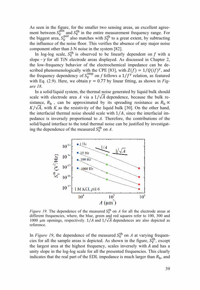
In a solid/liquid system, the thermal noise generated by liquid bulk should scale with electrode area A via a 1 √⁄ dependence, because the bulk re-sistance, , can be approximated by its spreading resistance as ∝√⁄ , with K as the resistivity of the liquid bulk [30]. On the other hand, the interfacial thermal noise should scale with 1⁄ , since the interfacial im-pedance is inversely proportional to A. Therefore, the contributions of the solid/liquid interface to the total thermal noise can be justified by investigat-ing the dependence of the measured on A.
Figure 19. The dependence of the measured on A for all the electrode areas at different frequencies, where, the blue, green and red squares refer to 100, 300 and 1000 µm openings, respectively. 1⁄ and 1 √⁄ dependences are also depicted as reference.
In Figure 19, the dependence of the measured on A at varying frequen-cies for all the sample areas is depicted. As shown in the figure, , except the largest area at the highest frequency, scales inversely with and has a unity slope in the log-log scale for all the presented frequencies. This clearly indicates that the real part of the EDL impedance is much larger than , and

40
thus the interfacial thermal noise, with respect to that of the liquid bulk, pre-vails in the given experimental conditions.
Since potVS is in a great accordance with as illustrated in Figure 18, it
can be inferred that the solid/liquid interfacial noise is subjected to the 1⁄ form, showing its association with complex electrochemical processes at the interfaces.
4.3.2. Significant extrinsic noise in ISFETs Finally, the area-normalized of the 300 µm diameter TiN electrode is compared, in Figure 20, to the area-normalized input-referred noise of sev-eral state-of-the-art MOSFETs [84]–[86]. The comparison is made at 1 Hz and 10 Hz and includes different combinations of KCl concentration and pH value for the TiN electrode. It is apparent that the EDL noise is comparable or even higher than that of the reported advanced MOSFETs and cannot be neglected. Additionally, when the KCl concentration was reduced from 1 M to 1 mM at pH=6 with a negligible proton concentration, the observed change in was too small to associate to an increase in by about three orders of magnitude. This further confirms the minor role of the noise gener-ated in the electrolyte bulk.
Figure 20. Comparison of area-normilized solid/liquid noise with the input-referred noise of several state-of-the-art MOSFETs at 1 and 10 Hz [84]–[86].
In contrast to the assumptions of others [30], [34], the real part of the meas-ured sample impedance is much larger than the liquid impedance. We specu-late that this is due to a rate limiting interfacial interaction or diffusion pro-cess at the liquid-solid boundary. It is striking, and has also been document-ed in the literature [82] that the voltage noise so closely follows the J-N for-mula. We believe that this is due to the fact that the presented oxide/liquid

41
system, measured under conditions of negligible current flow, is close to thermal equilibrium. Since the noise frequency dispersion is close to 1/f, it may be inferred that even 1/f noise obeys the J-N relation for systems close to thermal equilibrium. Another ubiquitous feature of these systems is the existence of the CPE with a phase between -π/4 and –π/2. No physical elec-trical network can give this relationship but it could be approximated by a non-uniform distributed network, which will be the topic of next chapter.

42
5. Electrochemical Impedance Modelling for Solid/Liquid Interface
In Chapter 4, it was concluded, from experimental viewpoint, that the LFN originating from the solid/liquid interface is of thermal nature, based on the excellent agreement between the potentiometric LFN and the real part of electrochemical impedance spectrum of the solid/liquid systems. Also, the interfacial noise was found to be subjected to a 1⁄ form. In order to un-cover the physics behind the 1⁄ nature of the interfacial noise, in this chapter an impedance model is developed, based on the dynamic hydrogen ion binding reactions at oxide/electrolyte interface. Firstly, the modeling process will be presented in Section 5.1. The validity of the proposed model will then be justified in section 5.2, taking ALD TiO2 films with different growth cycles as model samples.
5.1. Model development 5.1.1 Interfacial impedance based on site-binding reactions Modelling the dynamics of a system is concerned with solving the corre-sponding dynamic equations. The dynamic rate equations for the H+ site-binding reactions (2.2a) and (2.2b) are given as
-A S A
d[M-OH][M-O ] [M-OH] ,
dc a r
t= − (5.1a)
+
+2B S B 2
d[M-OH ][M-OH] [M-OH ]
dc a r
t= − (5.1b)
In the context of impedance modeling, the solving process focuses on find-ing the dynamic current-voltage relations. For the oxide/electrolyte interface, the dynamic current arising from the dynamic processes described with Eqs. (5.1a) and (5.1b) are:
0A S A S A
d[M-OH]( ),
dI q qN c a r
tΘ Θ−= = − (5.2a)
+
02B S B S B
d[M-OH ]( )
dI q qN c a r
tΘ Θ+= = − (5.2b)

43
where, Θ+ , Θ− , and 0Θ denote the fractions of protonated, deprotonated, and neutral OH groups, respectively. Θ+ , Θ− , and 0Θ can be expressed as [53]:
2
0S B SA B
1 1 1
, , ,a K aK K
D D DΘ Θ Θ+ −= = = (5.3)
where, aS, cA, cB, and D1 represent the same meanings respectively as in chapter 2. The solution of Eq. (5.2) is of the form of a two-branch admit-tance that naturally corresponds to the site-binding reaction, which can be solved by adding an AC voltage perturbation and making the small-signal approximation. The solving details can be found in Supporting Information (SI) of attached Paper III. The final expression for the site-binding admit-tance is:
S Abuff
2 A B
SB 2S B S A
1 A B 1 A B
11
1
a KsC s
D c cY
a K a Ks s
D c c D c c
+ +
= + ++ + +
(5.4)
where, s jω= with j as the imaginary unit and ω as angular frequency; buffC is the capacitance associated with the buffer capacity intβ , calculated with:
2
0 S S 2 B Sbuff int 2
S S 1
d d H
d d
p q N D K aC
kT D
σ βϕ ϕ
= = = (5.5)
The EDL capacitance DLC parallels with SBY network. Therefore, the to-
tal electrochemical impedance for the oxide/liquid interface, denoted as intZ , can be expressed as:
int
DL SB
1Z
sC Y=
+ (5.6)
5.1.2 Variability in surface properties It should be noted that a finite number of components appear in the circuit in Figure 21(a), which yields a semicircle centered on the x-axis in a Nyquist, and thus cannot interpret the CPE behaviors observed at the solid/liquid in-terfaces. A broad distribution of the surface properties needs to be taken into consideration in order to account for the CPE behavior, and it can be achieved by investigating possible mechanisms that would cause the varia-
44
tion of the kinetic parameters cA and cB, as well as thermodynamic parame-ters KA and KB.
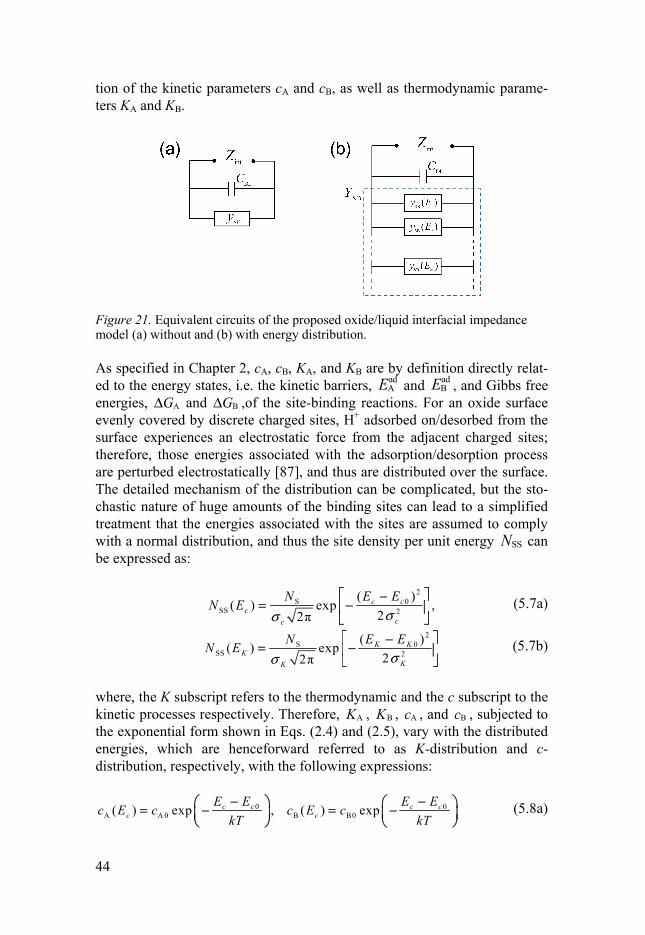
Figure 21. Equivalent circuits of the proposed oxide/liquid interfacial impedance model (a) without and (b) with energy distribution.
As specified in Chapter 2, cA, cB, KA, and KB are by definition directly relat-ed to the energy states, i.e. the kinetic barriers, ad
AE and adBE , and Gibbs free
energies, AGΔ and BGΔ ,of the site-binding reactions. For an oxide surface evenly covered by discrete charged sites, H+ adsorbed on/desorbed from the surface experiences an electrostatic force from the adjacent charged sites; therefore, those energies associated with the adsorption/desorption process are perturbed electrostatically [87], and thus are distributed over the surface. The detailed mechanism of the distribution can be complicated, but the sto-chastic nature of huge amounts of the binding sites can lead to a simplified treatment that the energies associated with the sites are assumed to comply with a normal distribution, and thus the site density per unit energy SSN can be expressed as:
2
S 0SS 2
( )( ) exp ,
22πc c
ccc
N E EN E
σσ −
= −
(5.7a)
2
S 0SS 2
( )( ) exp
22πK K
KKK
N E EN E
σσ −
= −
(5.7b)
where, the K subscript refers to the thermodynamic and the c subscript to the kinetic processes respectively. Therefore, AK , BK , Ac , and Bc , subjected to the exponential form shown in Eqs. (2.4) and (2.5), vary with the distributed energies, which are henceforward referred to as K-distribution and c-distribution, respectively, with the following expressions:
0 0A A 0 B B0( ) exp , ( ) expc c c c
c c
E E E Ec E c c E c
kT kT
− − = − = −
(5.8a)

45
0 0A A 0 B B0( ) exp , ( ) expK K K K
K K
E E E EK E K K E K
kT kT
− − = − = −
(5.8b)
in which, the subscript 0 refers the variables to their respective values at E0. Note that the K-distribution implies a distribution in the thermodynamic equilibria of the reactions, whereas the c-distribution implies that in their kinetic barrier.
In general, these four distributions may be correlated to any degree or in-dependent of each other. For simplicity in this treatment, the K-distributions, and likewise the c-distributions, are assumed to be completely correlated, while either the K or the c distributions will be investigated in turn, to see which matches the experimental data best.
Since SBY is a function of SN , Ac , Bc , AK , BK represented with Eqs. (5.3), it is also dependent on the distributed energy, so that intZ with the dis-tributed energies should be expressed as:
int
DL SB
1
( )dZ
sC y E E=
+ (5.9)
where, SBy denotes the density of SBY in the energy space. Eq. (5.9) is repre-sented with the equivalent circuit in Figure 21(b), with SBy represented as its discrete form.
5.2. Application of the proposed impedance model 5.2.1 Experimental procedure and parameter extraction TiO2 has received much attention in pH-sensing applications [77], [79], [88], due to its superior chemical and physical stability. Thus, it was chosen as our sampling oxide. Concerning the electrode fabrication, a 100 nm thick Ti layer was first sputter-deposited on a glass wafer, which was followed by the deposition of a 40 nm thick TiN layer in the same sputtering system but in the presence of N2. This was followed by ALD of TiO2 at 200 °C with TiCl4 and H2O as the reaction precursors. The deposition rate was estimated to be 0.045 nm per growth cycle by means of spectroscopic ellipsometry, yielding nominally a 1.8 nm thick TiO2 fil with 40 cycles. The wafer was then diced into 10 mm × 10 mm chips.
The schematic representation of the EIS measurement setup for the fabri-cated TiO2 chips is depicted in Figure 22(a). In the setup, the TiO2/TiN stack acts as the working electrode. The 0.2 M buffer solution (Merck Titrisol) was loaded in the reservoir glued on top of TiO2, while an Ag/AgCl/3 M NaCl

46
RE and a Pt electrode as a counter electrode were submerged in the buffer. The pH value of the sampling buffer was 7.
The open circuit voltage (OCV) on TiN was firstly recorded using the Bio-Logic VSP-300 potentiostat. When the OCV readout became stable, the EIS measurement was performed. The impedance spectrum was measured at 10 mV RMS AC from 100 mHz to 1 MHz. The measurement data was aver-aged over 30 cycles for each frequency point.
Figure 22. (a) Sketches of the electrode cell and the EIS measurement setup (b) Equivalent circuit of the buffer/TiO2/TiN impedance totZ , with S BY in its discrete representation.
Note that both the liquid bulk resistance bR and the TiO2 capacitance oxC are in series with intZ , as featured with the equivalent circuit in Figure 22 (b). The parameters of the impedance model for intZ proposed in section 5.1 can be extracted by numerically fitting the theoretical total impedance
tot int ox b1Z Z sC R= + + to the measurement data, with oxC and bR as mod-eling parameters as well. The details of the regression process can be found in SI of Paper III attached.
5.2.2. K-distribution vs c-distribution As mentioned in section 5.1, the validities of K- and c- distributions should be justified by evaluating which one fits the experimental data best. Hence, the simulated intZ , with either distribution considered at a time, is compared with experiment for the 40 cycle TiO2 at pH=7, as depicted in Figure 23. The optimized modeling parameters are summarized in Table 1, where,
S 10 SH log ( )p a= − , as well as + 0, , and Θ Θ Θ− calculated via Eq. (5.3), are also listed.

47
Figure 23. Comparison between simulation (curves and crosses) and measurement (squares and triangles) for the impedance with (i) the c-distribution and (ii) the K-distribution, depicted in (a) Bode plot and (b) Nyquist plot. Red symbols and curves refer to the K-distribution, while blue ones to the c-distribution. Black symbols refer to the measurement.
For the K-distribution, the simulation was also carried out with A0K and B0K as fitting parameters, depicted with red curves and crosses in plot ii) in
Figure 23(a) and (b). Although the fitting is fairly good, it leads to a 100% negatively charged surface and negative pK values in Table 1, which is physically unreasonable. In addition, the obtained pHS value at 13.4, as listed in Table 1, is unreasonably high, because it should be kept close to point of zero charge (PZC), around 6.2 for TiO2 via PZC=(pKA+pKB)/2, owing to the large intrinsic buffer capacity of the oxide. All these results invalidate the K-distribution.
For the c-distribution, the simulation agrees well with the measurement. As the black curve in the Nyquist diagram shown in Figure 23 (b) indicates, the proposed model accurately describes the CPE behavior of the TiO2/electrolyte interface. The resulting surface charging is in a thermody-namic favorable condition where only a small fraction of the OH group is charged with the occupancy of -O− site being slightly higher than that of
2-OH+ , as shown in Table 1. The fitted CDL value is comparable to our measured value of CDL ranging from 0.2 to 0.3 Fm-2 on a Pt electrode in the same solutions, as well as to the literature reported Stern capacitance CStern ranging from 0.2 to 1.4 Fm-2 [53]. Moreover, the extracted binding site den-sity 18 2
S 8.8 10 mN −= × is close to the reported range of 5-7× 18 210 m− for TiO2 anatase [89]–[91].

48
Table 1. Extracted modeling parameters for the K- and c-distributions for the 40 cycle TiO2 in a pH=7 buffer. KA0 and KB0 refer to the values of KA and KB at the energy centroid, and likewise cA0 and cB0 to cA and cB.
K-distribution c-distribution
Mod
elli
ng p
aram
eter
s Rb, Ω 68 68
Cox, Fm-2 0.34 0.52
CDL, Fm-2 0.37 0.26
, M-1s-2 2.8×10¹⁰ 80.1
, M-1s-2 5.4×10⁷ 3.0×10⁻⁴
pKA -3.2 7.7*
pKB -4.2 4.7*
aS 4.2×10⁻⁸ 0.57
NS, 10-18m-2 7.3×10⁶ 9.0
σK or σc, eV 0.18 0.18
Der
ived
pr
oper
ties pHS 13.4 6.24
Θ+ 0.0% 2.7%
Θ0 0.0% 94.0%
Θ- 100.0% 3.3%
* Specified as the reported values[89], [90] The better agreement achieved with the c-distribution than the K-
distribution indicates that the thermodynamic properties of the surface, rep-resented by AK and BK , tend to be uniform over the surface, while the ki-netic parameters would be strongly affected. This can be understood based on the notion that a conservative electrostatic potential can hardly change the Gibbs free energy of the binding reactions; the reaction kinetic barrier, how-ever, can be readily affected by such electrostatic forces.

49
6. Understanding Oxide/Electrolyte Interface Noise
Based on the impedance model proposed in the last chapter, various surface properties of the solid/liquid interface can be extracted by comparing the theoretical impedance to the measurement data. The LFN originating from the interface, in turn, is linked to these surface properties. In this chapter, a comprehensive discussion will be made regarding how the noise is affected by the dynamic properties of the oxide/electrolyte interfaces. Except for the 40 cycle sample presented in the last chapter, two more samples with 20 and 60 cycle fabricated under the same conditions are added in the analysis, in order to introduce varying surface potteries. In Section 6.1 the noise model-ing mothed will be analyzed. The results will then be presented and dis-cussed in Section 6.2.
6.1. Noise modeling analysis 6.1.1. Parameter extraction The main weakness of parameter extraction method for the proposed imped-ance model, as discussed in section 5.2.3, is the large number of parameters involved in the fitting procedure. In order to further constrain the modeling process, the values of Sa , SN , and DLC were solved by the classic SBM [53], with HpS was measured for all the TiO2 samples. The details can be found in SI of Paper IV appended. The oxide is believed not to contribute to the real part of the measured impedance, and then the noise of the TiO2/buffer systems is attributed merely to the interfacial effect, and oxC is on longer included for the noise analysis. Therefore, only A0c , B0c , and Eσ need to be determined numerically in terms of the noise analysis, and this can be achieved by numerically fitting the real part of Zint in Eq. (5.8) to that of the measured TiO2/buffer impedance. As mentioned at the beginning of this chapter, the 20 and 60 cycle samples fabricated in the same conditions are added in the analysis, in order to introduce varying surface potteries.
In Figure 24, the simulated interfacial noise nVS , calculated via
nV int( ) 4 Re[ ( )]S f kT Z f= , is depicted as a function of frequency, and com-
pared with experimental (calculated from the real part of the measured

50
Figure 24. Comparison between simulated noise spectrum density depicted as solid lines and the experimental data calculated from real part of the measured impedance, depicted as triangels, for all the samples. Black, red and blue represent 20, 40, and 60 cycle samples, respectively
impedance via the same equation) for all the samples at pH 7, in which the bulk resistance bR , extracted from high frequency data, has been subtracted. Note that excellent agreement is obtained in all cases. The values of all the modeling parameters are summarized in Table 2.
Table 2. Parameters for modeling the noise of the three processed samples at pH 7
Modelling para. Note 20 cycle 40 cycle 60 cycle
SpH, mV/pH Meas. 55.4 55 53.9
NS 1018
Calc. via SpH 10.0 9.0 7.0
CDL, Fm-2 0.26 0.26 0.26
pKA Reported [89], [90]
7.7 7.7 7.7
pKB 4.7 4.7 4.7
, M-1m-2 Numerical fitting
7.8×10⁻³ 78.8 7.5×10³
, M-1m-2 1.3×10⁻¹⁴ 2.4×10⁻⁴ 1.6×10²
σc, eV 0.327 0.179 0.116
6.1.2. Noise dependence on the site-binding admittance As discussed in Section 5.1, both the interfacial admittance SBY and DLC contribute to intZ , and thus the interfacial noise. A static aspect, DLC , how-ever, is not related to the surface dynamic properties. It is thus only SBY that reflects the contribution of the surface dynamics to the noise. For noise study, investigation of the real part of SBY , compared to its imaginary part, is

51
more instructive because the interfacial noise, nV int( ) 4 Re[ ( )]S f kT Z f= , is
linked to SBRe( )Y via the following expression:
int int SB2 2
int int
1 1Re( ) Re( ) Re( )Z Y Y
Y Y= = (6.1)
Hence, Re(YSB), instead of the noise per se, acts as an indicator for investi-gating the noise dependence on the dynamic properties, which avoids clumsy consideration of CDL. Specifically, the sample-dependent trend of Re(YSB) extracted from the measurement, as depicted in Figure 25(a), becomes the benchmark to which the trend of Re(YSB) calculated with the sample-dependent dynamic properties will be compared, as will be discussed mo-mentarily.
Figure 25. (a) Re(YSB) extracted from the EIS measurement at varying frequencies in order of the samples. (b) The dependance of Re(Zint) on Re(YSB) extracted from the EIS measurement at varying frequencies for all the samples, in which the dependance of Re(Zint) on Re(YSB) with Im(YSB) deliberately excluded is also depicted, shown as the solid curves.
The dependence of Re(Zint) on Re(YSB) extracted from the EIS measurement, as represented with the colored squares in Figure 25(b), can be analyzed semi-quantitatively by deliberately removing Im(YSB) from the Zin network, which is featured with equivalent circuit in the figure. As the solid curves representing the circuit shown in Figure 25(b), for all the presented frequen-cies, Re(Zint) linearly increases with Re(YSB), as Re(YSB) is smaller than ωCDL; but the trend reverses from linearly increasing to decreasing, as Re(YSB) goes beyond ωCDL. This predicted trend is followed well by the observed Re(Zint)–Re(YSB) relation, as shown in the figure. Therefore, the dependence of the noise on Re(YSB) is determined by the relative size of the susceptance of CDL to Re(YSB) .

52
6.1.3. Averaging of distributed interfacial properties As discussed in Section 5.1.2, the binding site density SN per unit energy, i.e. SSN , is subjected to the normally distributed kinetic barrier Ec. Since the corresponding reaction rate constants Ac and Bc are exponentially depend-ent on Ec, it is expected that only a portion of the sites can respond to the external stimulation of EIS measurement, and thus contribute to the noise at a certain frequency, and so do the values of Ac and Bc . One has to find out the representatives of these distributed properties for the whole surface, to order to facilitate the analysis of the noise dependence. This can be achieved by averaging their distributions with the distributed site-binding admittance ySB(Ec) as a weighting factor. Choosing ySB(Ec) as the weighting factor is based on the notion that the sites contribute to the noise by summing up ySB(Ec) over the surface. Owing to the same reason discussed in the last sub-section, Re[(ySB(Ec)] is used as the weighting factor.
Figure 26. Re[(ySB(Ec)] dependent on the reaction barreir Ec, at (a) 1 Hz and (b) 10 Hz for all the samples.
In Figure 26, Re[(ySB(Ec)] as a function of Ec is depicted at (a) 1 Hz and (b) 10 Hz, respectively. Only the sites SS( )cN E , and thus the corresponding

53
A ( )cc E and B ( )cc E , within the small ranges around the peaks of ySB(Ec) contribute effectively. Their averages, i.e. SSN , Ac and Bc , can then be calculated via:
0 0A A 0 B B 0exp , exp
c c c cE E E Ec c c c
kT kT
− −= = (6.2a)
2
0SSS 2exp
22πc c
cc
E ENN
σσ−
= − (6.2b)
where 0c cE E− is calculated with:
0 SB
0
SB
( ) R e ( ) d
R e ( ) d
c c c
c c
c
E E y E EE E
y E E
− − =
(6.3)
The average of ySB(E), i.e. SBy , can then be represented as well by substi-tuting SS( )N E , A ( )c E and B ( )c E in Eq. (5.4) with their average values.
6.2. Correlation of LFN to surface dynamic properties 6.2.1. Effect of reaction rate constant In Figure 27(a), Ac and Bc , calculated with Eq. (6.2a), are depicted in order of ALD samples at three different frequencies, 0.1, 1, and 10 Hz. As seen, both Ac and Bc are dependent on f; at a given f, Ac is almost identical for all samples independent of the number of deposition cycles, but
Bc increases by 10 orders of magnitude as the ALD process increases from 20 to 60 cycles. To elucidate this, the schematic frequency response of the real part of a single branch SBy is plotted in Figure 27(b), where SBRe( )Y, as the envelope of several SBy branches, is also plotted. It is seen that each branch contributes to SBRe( )Y mainly near its corner frequency fc, which corresponds to the admittance contribution within a narrow Ec range at a certain frequency, as shown in Figure 26. Therefore, at a given measurement frequency fM, only the branches that have fc close to fM will contribute to
SBRe( )Y . The relationship between fc and the surface properties was found to be proportional to A ( )cc E for any branch (see SI of Paper IV). Thus, at a specified fM, Ac should be proportional to fM, estimated as (see SI of Paper IV):
AS
2Mc f
a
π= (6.4)

54
Since Sa is kept constant by a large Cbuff for similar surfaces at the same pH, Ac will be determined mainly by fM and is not expected to vary much from
sample to sample. Eq. (6.4) also clearly indicates that at low fM, the sites with low Ac (high kinetic barrier Ec) contribute dominantly to SBRe( )Y and thus LFN, while those with high Ac (low Ec) contribute only at higher fM. However, since YSB is in parallel with CDL, the contribution from the sites with low Ec to the noise will be shorted by CDL at high frequencies. Since fc is observed to be independent of Bc , it becomes apparent that the –O- sites, rather than the neutral –OH sites, determine the surface dynamics and thus the noise, as a result of the much larger reaction rate of the –O- sites than that of the –OH sites. By substituting Ac and Bc for each samples in Eq. (5.4), 2
SS ( ) /q N E kT -normalized SBRe[ ]y is depicted in Figure 27(c) at the three frequencies. As seen, the increment of the normalized SBRe[ ]y at a given frequency is less than a factor of 2 from 20 to 60 growth cycles, which is the direct result of the invariability of Ac and thus distinctly dif-fers from the observed trend of SBRe( )Y in Figure 25(a).
Figure 27. (a) Sample-dependent Ac and Bc at varying frequencies. (b) Sche-matic frequency responses of SBRe( )y and SBRe( )Y . Details of the equivalent circuit of the single branch can be found in Paper III. (c) NSS-normalized SBRe[ ]y in order of the samples at the three different frequencies.s

55
6.2.2. Effect of site density As for the contribution of SSN to the interfacial LFN, similar to Ac and
Bc , SSN was first calculated via Eq. (6.2b) and then depicted in order of samples at varying frequencies in Figure 28(a). As depicted in the figure,
SSN increases from 20 to 60 cycles sample at a certain f. Using Ac and Bc , SBRe[ ]y was calculated and depicted in order of samples at the three
frequencies in Figure 28(b). SBRe[ ]y resembles well the observed sample-dependent variation of SBRe( )Y in Figure 25(a). Since the variations of Ac and Bc hardly interpret the trend of SBRe( )Y , the variation of SSN should account for it, and thus for the LFN.
Figure 28. Figure 6. (a) SSN and (b) SBRe( )y calculated with SSN , Ac and
Bc at varying frequencies in (b).
6.2.3. Summarized remarks As shown in Figure 29 with three site-binding branches characterized by Ec1 to Ec3 for illustration, the noise spectrum envelope consists of contributions from distributed site-binding branches with different kinetic barriers Ec. It is the sites with large Ec that would contribute most to the noise in the low-frequency regime; the amplitude of the LFN is primarily determined by Nss with large Ec. Therefore, to minimize the LFN, reducing the Nss with large Ec can be an effective approach.

56
Figure 29. Schematic dependence of LFN on Ec, as well as and its freqeuncy spectrum. The three colored lines illustrate contributions from three site-binding reaction branches with different kinetic energy barriers, Ec1, Ec2, and Ec3.

57
7. Concluding Remarks and Future Perspective
In summary, this thesis peruses an insightful understanding of the LFN aris-ing in ion sensing devices, with ISFETs as a particular focus. For this pur-pose, the research work starts firstly with the discussion of the proposed semiconductor device for an enhanced SNR for the ISFETs. Then, the fabri-cation and characterization of the differential microelectrode array archives the accurate measurement of solid/liquid interfacial noise. At the end, elec-trochemical impedance model is developed based on the interfacial proper-ties for interpreting the interfacial noise, which is immediately followed by a thorough discussion about the dependence of the noise on the surface dy-namic properties. Upon the extensive work, the major achievements are summarized as follows:
1. Motivated with the internal amplification to diminish the external inter-ference, the IGBA device was designed and fabricated, which is featured with the intimate integration of an ISFET with a low-noise vertical BJT. The internal amplification was achieved by the immediate and direct current am-plification of the BJT, yielding a 70-fold internal current gain, and the IG-BA’s efficacy of enhancing SNR was clearly demonstrated by comparing its noise performance to that of the ISFET alone. The high current gain also applies when the device is used for pH sensing. These characteristics make the IGBA competitive in applications such as genome sequencing which are prone to be affected by the external interference owing to a dense integration of ion sensors.
2. The differential microelectrode array was fabricated, and the sol-id/liquid interfacial noise was accurately assessed based on the fabricated cell. The characterization incorporated both potentiometry and EIS concur-rently for the noise measurement. The measured poteiometric noise is found to coincide quantitatively with the thermal noise calculated from the meas-ured impedance, evidencing the noise originating from the TiN/electrolyte interface is of thermal nature.
3. The solid/liquid interface noise is found to be comparable or even larg-er than the input-referred noise of the state-of-the-art MOSFETs. Therefore, its influence cannot be overlooked for design of future ion sensors
4. Based on the SBM describing the H+ reactivity at the oxide/liquid inter-faces, a dedicated electrochemical impedance model was derived. The model not only incorporates both thermodynamic and kinetic properties of the site-binding reactions, but further takes into consideration the distributed nature

58
of the characteristic energy of the binding sites, so as to account for the inter-facial impedance featured with the CPE behavior. With the model, the sol-id/liquid interfacial LFN is clearly linked to the thermodynamic and kinetic properties of the oxide surface.
5. The derived impedance model was used to investigate the correlation of the LFN to the averaged reaction rate constants and binding site density. Ac is found to be determined mainly by the measurement frequency fM. At a given fM, it will not vary too much among samples, and thus cannot account for the corresponding noise variation.
6. The noise spectrum consists of contributions from distributed site-binding branches with different kinetic barriers Ec. It is the sites with large Ec that would contribute dominantly to the noise in the low-frequency re-gime; the amplitude of the LFN is primarily determined by Nss with large Ec.
Through this work, the extensive knowledge regarding the origination and mechanism of the noise of solid/liquid systems has been gained, being a dispensable step towards even more insightful understanding of the sol-id/liquid systems. To this end, extra efforts can be placed as follows:
1. The extended-gate configuration can be integrated tightly with the IG-BA devices in the same chip, in order to minimize any possible coupling of external interference. On the other hand, the integration of the two compo-nents as a robust pH measurement platform has vast potential to benefit the corresponding sensing applications.
2. The over-simplified model for super thin oxide layers would limit ap-plication of the proposed interfacial impedance model. A more accurate model can be applied to the oxide, which should be assisted with more de-tailed characterizations on the oxide surface morphology, thickness and die-lectric properties etc.
3. It is intereting to explore other mechanisms behind the distributed en-ergy proposed in the model than the static charging on the surface. In partic-ular, the physical meaning of σc can be explored.
4. It is interesting to explore the dependence of the solid/liquid interfacial noise on the interfacial thermodynamic properties, i.e. KA and KB, which can be performed by investigating the solid/liquid noise of varying oxides.

59
Summary of the Appended Papers
Paper I presents an ion-gated bipolar amplifier (IGBA) featured with inter-nal current amplification. The IGBA device, fabricated with standard CMOS technology, consist of an ISFET tightly integrated with a low-noise vertical BJT for internally amplifying signal current from the ISFET up to 70-fold. The internal amplification significantly suppresses the interference from external noise, which leads to an SNR improvement compared to its ISFET reference. The high current gain also applies when the device is used for pH sensing. Applications like genome sequencing are susceptible to the external interference due to a dense integration of huge amount of sensors. Thus, the efficacy of suppressing external interference makes the IGBA-based sensors suitable for these applications.
Paper II presents the fabrication and characterization of a microelectrode cell dedicated for assessment of the solid/liquid interface noise without re-course to a reference electrode. In the electrode cell, two identical TiN elec-trodes of various sizes are designed for differential measurements. Both po-tentiometry and EIS were applied to the fabricated electrode cell for the as-sessing the interfacial noise. The measured poteiometric noise almost equals to the thermal noise calculated from the measured impedance, indicating the noise from the TiN/electrolyte system is of thermal nature. Scaling inversely with electrode area, the noise is concluded to mainly arise from the solid–liquid interface. Besides, the solid/liquid interface noise is found to be com-parable or even larger than the input-referred noise of the state-of-the-art MOSFETs. Therefore, its influence cannot be overlooked for design of fu-ture ion sensors
In Paper III, a dedicated electrochemical impedance model is developed, based on the H+ reactivity at the oxide/liquid interfaces described by the SBM. The model is derived from the dynamic rate equations of the ampho-teric H+ site-binding reactions, incorporating both thermodynamic and kinet-ic properties of the reactions. By taking into account the distributed nature of the kinetic barriers of the binding sites, the model is found to give an excel-lent agreement with the measured impedance including attaining reasonable modeling parameters, which confirms that the CPE behavior of the sol-id/liquid interface can be accounted for by the variability of the kinetic barri-ers of the H+ site-binding reactions. With the model, the solid/liquid interfa-cial LFN is linked to the thermodynamic and kinetic properties of the oxide surface.

60
Paper IV investigates the dependence of the noise on the averaged reaction rate constants and binding site density by using the impedance model devel-oped in Paper III. The study unveils that the variation of interfacial noise is primarily caused by that of averaged binding site density, rather than the reaction rate constants. The sites with large kinetic barriers Ec that would contribute dominantly to the noise in the low-frequency regime; the ampli-tude of the LFN is primarily determined by Nss with large Ec. Therefore, to minimize the LFN, reducing the Nss with large Ec can be an effective ap-proach.

61
Sammanfattning på svenska
Den enorma vetenskaplig och kommersiell betydelse som finns av att de-chiffrera den mänskliga genetiska koden har startat en revolution inom ge-nom-sekvenseringstekniken. Den första fullständiga sekvenseringen av män-niskans genom uppnåddes genom det humana genomprojekt (HGP) 2003, då genom att använda den traditionella Sanger-metoden. Under årtiondena efter HGP hade slutförts kom en uppsjö av tekniska innovationer ut till forsk-ningsgemenskapen och sekvenseringsmarknaden. Alla dessa innovativa se-kvenseringstekniker har bidragit till betydligt kortare testtider och till lägre kostnader jämfört med de traditionella metoderna, detta tyder på en framtid med prisvärd personlig diagnostik och behandling.
Jon Torrent-sekvenseringstekniken, en av de nyaste sekvenseringsme-toderna, har haft en stor påverkan på sekvenseringsfältet. Detta på grund av dess förmåga att integrera ytplacerade sensorer med avläsningskretsar på baksidan, tillverkade med CMOS-tekniken. Sekvenseringsprincipen för Jon Torrent-metoden är enkel. Det enkelsträngade DNA:t utsätts sekventiellt för de fyra typerna av deoxinukleosidtrifosfat (dNTP), A, C, G eller T. När en inkommande dNTP är komplementär till nästa icke-parade nukleotid på DNA kedjan reagerar dom och frigör en proton (H+) som sedan kan detekte-ras av proton -sensorer.
De protonsensorerna som används i Jon Torrent-sekvensering är jonkäns-liga fälteffekttransistorer (ISFET). En ISFET är en halvledarkomponent som kan tillverkas med standard CMOS-teknik. Vanligtvis tillverkas dessa av ett måttligt dopat kiselsubstrat med två kraftigt dopade områden i motsatt pola-ritet till substratet, dessa verkar som source och drain. Mellan source och drain går det en ledande kanal med ett lager av oxid ovanpå. Under en mät-ning sätts oxidytan i kontakt med en vätska och när vätskans pH varierar för att bibehålla ytjämvikten kan de amfotära hydroxyl (OH) -grupperna på oxidytan fånga/släppa protonerna. Som följd av denna mekanism uppstår det en variation i ytladdningen. Sålunda kommer oxidens elektriska potential φ0
att förändras och den förändringen kommer att påverka kanalen under oxid-en, vilket orsakar en ändring i kanalens genomsläppta ström (ID). Förståelse för operationsprincipen hos en ISFET är beroende av hur φ0 varierar med pH:t. Detta har väl beskrivits genom platsbindningsmodellen (SBM) som beskriver hur proton-reaktiviteten vid oxid/vätskegränsskiktet korrekt kan kvantifieras.

62
Däremot är det inte så att integreringen av flera sensorer alltid är till nå-gon fördel. Försämringen av brusprestandan för ISFET-enheterna och allvar-liga internkontamineringar mellan de integrerade kretsarna kan markant på-verka sekvenseringsnoggrannheten. För Jon Torrent-sekvenseringen betyder en enkelbaskoppling till DNA:t en förändring av 0,02 i pH:t, detta motsvarar omkring 1 mV-förändring i φ0 enligt Nernst-ekvationen. För att mäta en sådan liten potentiell förändring så måste bruset i sensorn sänkas till en ac-ceptabel nivå. Den största delen av bruset i jonavkännande komponenter kan ses i lågfrekvensregimen, det är också där sensorexperimenten typiskt utförs. Dessutom så kan en hög densitet av metall delar i sensorchipset resultera i lågfrekventa interferenser som kan störa de biomedicinska signalerna som finns i samma frekvensdomän. Därför blir lågfrekvent brus (LFN) en av de viktigaste prestanda parametrarna för jonkänsliga FET-system
För ett ISFET-baserat sensorsystem kan bruset ha sitt ursprung utanför sensor, från t.ex. omgivningen och mätinstrumenten. Dessa yttre källor kan försummas genom att internt förstärka ISFET:s signaler, vilket förbättrar det mätta signal-brusförhållandet (SNR). Med den motiveringen av behovet av intern signalförstärkning designade och tillverkades nya jonavsensorer, dvs jonkontrollerad bipolär förstärkare (IGBA). IGBA-enheten är utrustad med en nära integration med en ISFET och en brusdämpande vertikal bipolär förbindelsestransistor (BJT). Den interna förstärkningen uppnåddes genom omedelbar och direkt koppling till BJT:n, vilket gav en 70-faldig intern-strömförstärkning. IGBA: s effektivitet för förbättring av SNR visades tyd-ligt genom att jämföra dess brusprestanda mot den av en ensam ISFET. Hög-strömförstärkningen gäller också när enheten används för pH-mätningar. Dessa egenskaper gör den IGBA-baserade jonsensorn särskilt attraktiv inom områden som genom-sekvensering vilket kräver storskaliga, tättintegrerade jon-sensorer som kan snabbt generera en stor mängd data.
Brus inuti en ISFET kallas för ISFET:s interna brus. För de olika interna bruskällorna saknas det en systematisk studie för det fasta/flytande gränssnit-tet. För att exakt kunna bedöma gränssnittet i en LFN tillverkades en specifik differential-mikroelektrodmatris som användes för att karakterisera TiN/elektrolytgränssnittet. Karakteriseringen av bruset bestod av både poten-tiometri och elektrokemisk impedansspektroskopi. Det uppmätta potentio-metriska bruset visade sig sammanfalla kvantitativt med det termiska bruset beräknat från den reella delen av den uppmätta impedansen. Detta visar att LFN som kommer från TiN/elektrolytgränssnittet är av termisk natur. Dessu-tom så är gränssnittsbruset jämförbart och till och med större än det mätta bruset från toppmoderna MOSFET:s. Denna felkälla kan därför inte förbises för design av framtida jon-sensorer
Bortsett från experimentella resultat ger den här avhandlingen en inblick i förståelsen av LFN som kommer från den jon interaktionen vid det fasta/flytande gränssnittet. För att klargöra detta presenteras här en elektro-kemisk impedansmodell baserad på de gränssnittsegenskaperna som kan
63
resultera i gränssnittets LFN. Modellen innefattar inte bara de termodyna-miska och kinetiska egenskaperna hos de adsorberande reaktionerna utan tar även hänsyn till den karakteristiska naturen hos bindningssätena. Detta tillå-ter modellen att hantera gränssnittsimpedansen som presenteras med det konstanta faselementets beteende. Med modellen är det fasta/flytande gräns-snittens beteende uppenbart kopplat till de termodynamiska och kinetiska egenskaperna hos oxidytan.
Den härledda impedansmodellen användes för att undersöka om bruset var beroendet av de genomsnittliga reaktionshastighetskonstanterna och bindningsstätheten. Det visade sig att variationen av gränssnittsstörningar huvudsakligen orsakades av den genomsnittliga bindningsställdensitet sna-rare än reaktionshastighetskonstanterna
Genom detta arbete har den omfattande kunskapen om brusets uppkomst och mekanism utvecklats, vilket är ett viktigt steg mot ännu mer insikt och förståelse av fasta/flytande gränsskikt.

64
Acknowledgement
I would like to express my deep appreciation and thanks to my advisor Do-cent Zhen Zhang. You gave helping hands when I was in a mess and had been supporting me through these tough years. I can’t do this without you. Thank you! I want to specially thank Professor Shili Zhang for giving me the chance to come to Sweden, which opens up a special phase of my life that means a lot to me. Also, I have learnt a lot from you about how to survive in the compet-ing academia, which is really appreciated. Dr. Paul Solomon is the one to who I couldn’t express more gratitude. You teach me science with inconceivable patience. It is you who guides me to complete every task in the doctoral project. You have been a tremendous mentor for me. China scholarship council is highly appreciated for the financial support via a scholarship. I would also like to thank Dr. Michel Calame for being the opponent to my defense. I’ve learnt a lot from them when I visited his group. Other defense committee members are greatly appreciated too. Special thanks are given to Dr. Hans Norström, Dr. Uwe Zimmermann and Professor Jörgen Olsson for helping me and giving advises from time to time. Dr. Uwe Zimmermann and Professor Jörgen Olsson are also thanked for screening my thesis. Thanks are also given to Dr. Tomas Kubart and Dr. Jonathan Scragg for helping with TiN/TiO2 deposition. Dr. Carl Hägglund is also appreciated for the ellipsometry characterization. I’m grateful to my group (former) fellows for being there and helping me. They are Dr. Si Chen, Dr. Xindong Gao, Dr. Zhiying Liu, Dr. Indrek Must, Dr. Nathan Netzer, Dr. Asta Makaravičiūtė, Dr. Shabnam Mardani, Xi Chen, Lukas Joblonka, Shuangshuang Zeng, Xingxing Xu, Chenyu Wen, Qitao Hu, Shiyu Li, Reza Moossavi, Elis Nycander.

65
Thanks are also given the Carbon group (former) members, Docent Zhibin Zhang, Dr. Seung-Hee Jeong, Dr. Patrik Ahlberg, Dr. Malkolm Hinnemo and Jie Zhao for their helps.
I’m grateful to other colleagues at FTE division. MSL staff is also appreciat-ed for their help in the cleanroom. Zhang Peng & Guo Yan, Ren Yi & Li Xiaowen, Chen Song & Li Shu, Lingguang Li, Xie Yuan & Wang Hao, Li Hu, Jiao Mingzhi, Huang Wen, I would like to thank you all for accompanying and encouraging me. A special thanks to my family. 爸爸妈妈谢谢你们的支持,鼓励,宽容,理解。三言两语无法表达我的感激之情。希望你们长命百岁,我爱你们。
I want to say“thank you”to Song Man, for being the best friend, wife and Hanna’s mother. Most importantly, thank you for being you who I love.

66
Reference
[1] B. J. West and M. Shlesinger, “The Noise in Natural Phenomena,” Am. Sci., vol. 78, no. 1, pp. 40–45, 1990.
[2] J. C. Venter, M. D. Adams, E. W. Myers, P. W. Li, R. J. Mural, G. G. Sutton, H. O. Smith, M. Yandell, C. A. Evans, R. A. Holt, J. D. Gocayne, P. Amanatides, R. M. Ballew, D. H. Huson, J. R. Wortman, Q. Zhang, C. D. Kodira, X. H. Zheng, L. Chen, M. Skupski, G. Subramanian, P. D. Thomas, J. Zhang, G. L. Gabor Miklos, C. Nelson, S. Broder, A. G. Clark, J. Nadeau, V. A. McKusick, N. Zinder, A. J. Levine, R. J. Roberts, M. Simon, C. Slayman, M. Hunkapiller, R. Bolanos, A. Delcher, I. Dew, D. Fasulo, M. Flanigan, L. Florea, A. Halpern, S. Hannenhalli, S. Kravitz, S. Levy, C. Mobarry, K. Reinert, K. Remington, J. Abu-Threideh, E. Beasley, K. Biddick, V. Bonazzi, R. Brandon, M. Cargill, I. Chandramouliswaran, R. Charlab, K. Chaturvedi, Z. Deng, V. Di Francesco, P. Dunn, K. Eilbeck, C. Evangelista, A. E. Gabrielian, W. Gan, W. Ge, F. Gong, Z. Gu, P. Guan, T. J. Heiman, M. E. Higgins, R.-R. Ji, Z. Ke, K. A. Ketchum, Z. Lai, Y. Lei, Z. Li, J. Li, Y. Liang, X. Lin, F. Lu, G. V Merkulov, N. Milshina, H. M. Moore, A. K. Naik, V. A. Narayan, B. Neelam, D. Nusskern, D. B. Rusch, S. Salzberg, W. Shao, B. Shue, J. Sun, Z. Y. Wang, A. Wang, X. Wang, J. Wang, M.-H. Wei, R. Wides, C. Xiao, C. Yan, A. Yao, J. Ye, M. Zhan, W. Zhang, H. Zhang, Q. Zhao, L. Zheng, F. Zhong, W. Zhong, S. C. Zhu, S. Zhao, D. Gilbert, S. Baumhueter, G. Spier, C. Carter, A. Cravchik, T. Woodage, F. Ali, H. An, A. Awe, D. Baldwin, H. Baden, M. Barnstead, I. Barrow, K. Beeson, D. Busam, A. Carver, A. Center, M. L. Cheng, L. Curry, S. Danaher, L. Davenport, R. Desilets, S. Dietz, K. Dodson, L. Doup, S. Ferriera, N. Garg, A. Gluecksmann, B. Hart, J. Haynes, C. Haynes, C. Heiner, S. Hladun, D. Hostin, J. Houck, T. Howland, C. Ibegwam, J. Johnson, F. Kalush, L. Kline, S. Koduru, A. Love, F. Mann, D. May, S. McCawley, T. McIntosh, I. McMullen, M. Moy, L. Moy, B. Murphy, K. Nelson, C. Pfannkoch, E. Pratts, V. Puri, H. Qureshi, M. Reardon, R. Rodriguez, Y.-H. Rogers, D. Romblad, B. Ruhfel, R. Scott, C. Sitter, M. Smallwood, E. Stewart, R. Strong, E. Suh, R. Thomas, N. N. Tint, S. Tse, C. Vech, G. Wang, J. Wetter, S. Williams, M. Williams, S. Windsor, E. Winn-Deen, K. Wolfe, J. Zaveri, K. Zaveri, J. F. Abril, R. Guigó, M. J. Campbell, K. V Sjolander, B. Karlak, A. Kejariwal, H. Mi, B. Lazareva, T. Hatton, A. Narechania, K. Diemer, A. Muruganujan, N. Guo, S. Sato, V. Bafna, S. Istrail, R. Lippert, R.

67
Schwartz, B. Walenz, S. Yooseph, D. Allen, A. Basu, J. Baxendale, L. Blick, M. Caminha, J. Carnes-Stine, P. Caulk, Y.-H. Chiang, M. Coyne, C. Dahlke, A. D. Mays, M. Dombroski, M. Donnelly, D. Ely, S. Esparham, C. Fosler, H. Gire, S. Glanowski, K. Glasser, A. Glodek, M. Gorokhov, K. Graham, B. Gropman, M. Harris, J. Heil, S. Henderson, J. Hoover, D. Jennings, C. Jordan, J. Jordan, J. Kasha, L. Kagan, C. Kraft, A. Levitsky, M. Lewis, X. Liu, J. Lopez, D. Ma, W. Majoros, J. McDaniel, S. Murphy, M. Newman, T. Nguyen, N. Nguyen, M. Nodell, S. Pan, J. Peck, M. Peterson, W. Rowe, R. Sanders, J. Scott, M. Simpson, T. Smith, A. Sprague, T. Stockwell, R. Turner, E. Venter, M. Wang, M. Wen, D. Wu, M. Wu, A. Xia, A. Zandieh, and X. Zhu, “The Sequence of the Human Genome,” Science (80-. )., vol. 291, no. 5507, p. 1304 LP-1351, Feb. 2001.
[3] D. J. Lockhart, H. Dong, M. C. Byrne, M. T. Follettie, M. V Gallo, M. S. Chee, M. Mittmann, C. Wang, M. Kobayashi, H. Norton, and E. L. Brown, “Expression monitoring by hybridization to high-density oligonucleotide arrays,” Nat Biotech, vol. 14, no. 13, pp. 1675–1680, Dec. 1996.
[4] K. V Voelkerding, S. A. Dames, and J. D. Durtschi, “Next-Generation Sequencing: From Basic Research to Diagnostics,” Clin. Chem., vol. 55, no. 4, p. 641 LP-658, Mar. 2009.
[5] F. Sanger, S. Nicklen, and A. R. Coulson, “DNA sequencing with chain-terminating inhibitors,” Proc. Natl. Acad. Sci. U. S. A., vol. 74, no. 12, pp. 5463–5467, Dec. 1977.
[6] F. Sanger and A. R. Coulson, “A rapid method for determining sequences in DNA by primed synthesis with DNA polymerase,” J. Mol. Biol., vol. 94, no. 3, pp. 441–448, 1975.
[7] J. Schmutz, J. Wheeler, J. Grimwood, M. Dickson, J. Yang, C. Caoile, E. Bajorek, S. Black, Y. M. Chan, M. Denys, J. Escobar, D. Flowers, D. Fotopulos, C. Garcia, M. Gomez, E. Gonzales, L. Haydu, F. Lopez, L. Ramirez, J. Retterer, A. Rodriguez, S. Rogers, A. Salazar, M. Tsai, and R. M. Myers, “Quality assessment of the human genome sequence,” Nature, vol. 429, no. 6990, pp. 365–368, May 2004.
[8] A. McKenna, M. Hanna, E. Banks, A. Sivachenko, K. Cibulskis, A. Kernytsky, K. Garimella, D. Altshuler, S. Gabriel, M. Daly, and M. A. DePristo, “The Genome Analysis Toolkit: A MapReduce framework for analyzing next-generation DNA sequencing data,” Genome Res. , vol. 20, no. 9, pp. 1297–1303, Sep. 2010.
[9] M. L. Metzker, “Sequencing technologies [mdash] the next generation,” Nat Rev Genet, vol. 11, no. 1, pp. 31–46, Jan. 2010.
[10] J. Shendure and H. Ji, “Next-generation DNA sequencing,” Nat Biotech, vol. 26, no. 10, pp. 1135–1145, Oct. 2008.
[11] E. R. Mardis, “Next-Generation Sequencing Platforms,” Annu. Rev. Anal. Chem., vol. 6, no. 1, pp. 287–303, Jun. 2013.
[12] D. C. Koboldt, K. M. Steinberg, D. E. Larson, R. K. Wilson, and E. Mardis, “The Next-Generation Sequencing Revolution and Its Impact on Genomics,” Cell, vol. 155, no. 1, pp. 27–38, Sep. 2013.

68
[13] K. Wetterstrand, “DNA Sequencing Costs: Data from the NHGRI Genome Sequencing Program (GSP).” [Online]. Available: www.genome.gov/sequencingcostsdata.
[14] T. Tucker, M. Marra, and J. M. Friedman, “Massively Parallel Sequencing: The Next Big Thing in Genetic Medicine,” Am. J. Hum. Genet., vol. 85, no. 2, pp. 142–154, Aug. 2009.
[15] J. R. ten Bosch and W. W. Grody, “Keeping Up With the Next Generation: Massively Parallel Sequencing in Clinical Diagnostics,” J. Mol. Diagn., vol. 10, no. 6, pp. 484–492, Nov. 2008.
[16] J. M. Rothberg, W. Hinz, T. M. Rearick, J. Schultz, W. Mileski, M. Davey, J. H. Leamon, K. Johnson, M. J. Milgrew, M. Edwards, J. Hoon, J. F. Simons, D. Marran, J. W. Myers, J. F. Davidson, A. Branting, J. R. Nobile, B. P. Puc, D. Light, T. a Clark, M. Huber, J. T. Branciforte, I. B. Stoner, S. E. Cawley, M. Lyons, Y. Fu, N. Homer, M. Sedova, X. Miao, B. Reed, J. Sabina, E. Feierstein, M. Schorn, M. Alanjary, E. Dimalanta, D. Dressman, R. Kasinskas, T. Sokolsky, J. a Fidanza, E. Namsaraev, K. J. McKernan, A. Williams, G. T. Roth, and J. Bustillo, “An integrated semiconductor device enabling non-optical genome sequencing.,” Nature, vol. 475, no. 7356, pp. 348–352, 2011.
[17] M. A. Quail, M. Smith, P. Coupland, T. D. Otto, S. R. Harris, T. R. Connor, A. Bertoni, H. P. Swerdlow, and Y. Gu, “A tale of three next generation sequencing platforms: comparison of Ion Torrent, Pacific Biosciences and Illumina MiSeq sequencers,” BMC Genomics, vol. 13, no. 1, p. 341, 2012.
[18] E. Pennisi, “Semiconductors Inspire New Sequencing Technologies,” Science (80-. )., vol. 327, no. 5970, p. 1190 LP-1190, Mar. 2010.
[19] L. Mamanova, R. M. Andrews, K. D. James, E. M. Sheridan, P. D. Ellis, C. F. Langford, T. W. Ost, J. E. Collins, and D. J. Turner, “FRT-seq: amplification-free, strand-specific transcriptome sequencing,” Nat Methods, vol. 7, 2010.
[20] N. Rusk, “Torrents of sequence,” Nat Meth, vol. 8, no. 1, p. 44, Jan. 2011.
[21] L.-T. Yin, J.-C. Chou, W.-Y. Chung, T.-P. Sun, and S.-K. Hsiung, “Separate structure extended gate H+-ion sensitive field effect transistor on a glass substrate,” Sensors Actuators B Chem., vol. 71, no. 1, pp. 106–111, 2000.
[22] J. van der spiegel, I. Lauks, P. Chan, and D. Babic, “The extended gate chemically sensitive field effect transistor as multi-species microprobe,” Sensors and Actuators, vol. 4, no. C, 1983.
[23] P. D. Batista and M. Mulato, “ZnO extended-gate field-effect transistors as pH sensors,” Appl. Phys. Lett., vol. 87, no. 14, p. 143508, Sep. 2005.
[24] S. M. Sze and K. K. Ng, Physics of Semiconductor Devices, 3rd ed. Wiley, 2006.
[25] L. DeFrancesco, “Life Technologies promises [dollar]1,000 genome,” Nat Biotech, vol. 30, no. 2, p. 126, Feb. 2012.

69
[26] I. Heller, S. Chatoor, J. M??nnik, M. A. G. Zevenbergen, J. B. Oostinga, A. F. Morpurgo, C. Dekker, and S. G. Lemay, “Charge noise in graphene transistors,” Nano Lett., vol. 10, no. 5, pp. 1563–1567, 2010.
[27] R. R. Harrison, “The Design of Integrated Circuits to Observe Brain Activity,” Proceedings of the IEEE, vol. 96, no. 7. pp. 1203–1216, 2008.
[28] C. G. Jakobson and Y. Nemirovsky, “I/f noise in ion sensitive field effect transistors from subthreshold to saturation,” IEEE Trans. Electron Devices, vol. 46, no. 1, pp. 259–261, 1999.
[29] A. Hassibi, R. Navid, R. W. Dutton, and T. H. Lee, “Comprehensive study of noise processes in electrode electrolyte interfaces,” J. Appl. Phys., vol. 96, no. 2, pp. 1074–1082, 2004.
[30] M. J. Deen, M. W. Shinwari, J. C. Ranuárez, and D. Landheer, “Noise considerations in field-effect biosensors,” J. Appl. Phys., vol. 100, no. 7, pp. 74703–74708, 2006.
[31] N. K. Rajan, D. A. Routenberg, J. Chen, and M. A. Reed, “1/f noise of silicon nanowire BioFETs,” IEEE Electron Device Lett., vol. 31, no. 6, pp. 615–617, 2010.
[32] N. K. Rajan, D. A. Routenberg, and M. A. Reed, “Optimal signal-to-noise ratio for silicon nanowire biochemical sensors,” Appl. Phys. Lett., vol. 98, no. 26, pp. 2–4, 2011.
[33] A. Tarasov, W. Fu, O. Knopfmacher, J. Brunner, M. Calame, and C. Schönenberger, “Signal-to-noise ratio in dual-gated silicon nanoribbon field-effect sensors,” Appl. Phys. Lett., vol. 98, no. 1, pp. 2011–2014, 2011.
[34] J. Go, P. R. Nair, and M. A. Alam, “Theory of signal and noise in double-gated nanoscale electronic pH sensors,” J. Appl. Phys., vol. 112, no. 3, p. 34516, 2012.
[35] D. Zhang, X. Gao, S. Chen, H. Norstr??m, U. Smith, P. Solomon, S. L. Zhang, and Z. Zhang, “An ion-gated bipolar amplifier for ion sensing with enhanced signal and improved noise performance,” Appl. Phys. Lett., vol. 105, no. 8, p. 82102, 2014.
[36] K. Bedner, V. A. Guzenko, A. Tarasov, M. Wipf, R. L. Stoop, S. Rigante, J. Brunner, W. Fu, C. David, M. Calame, J. Gobrecht, and C. Schönenberger, “Investigation of the dominant 1/f noise source in silicon nanowire sensors,” Sensors Actuators, B Chem., vol. 191, pp. 270–275, 2014.
[37] D. Zhang, I. Must, N. L. Netzer, X. Xu, P. Solomon, S. L. Zhang, and Z. Zhang, “Direct assessment of solid-liquid interface noise in ion sensing using a differential method,” Appl. Phys. Lett., vol. 108, no. 15, p. 151603, Apr. 2016.
[38] J. Zhuge, R. Wang, R. Huang, Y. Tian, L. Zhang, D. W. Kim, D. Park, and Y. Wang, “Investigation of Low-Frequency Noise in Silicon Nanowire MOSFETs,” IEEE Electron Device Letters, vol. 30, no. 1. pp. 57–60, 2009.
[39] A. Haemmerli, J. Janata, and J. J. Brophy, “Equilibrium Noise in Ion Selective Field Effect Transistors,” J. Electrochem. Soc., vol. 129, no. 10, pp. 2306–2312, Oct. 1982.

70
[40] P. R. Barabash and R. S. C. Cobbold, “Basic limitations of isfet and silicon pressure transducers: noise theory, models and device scaling,” Sensors and Actuators, vol. 4, no. C, pp. 427–438, Jan. 1983.
[41] M. V. Hauf, L. H. Hess, J. Howgate, M. Dankerl, M. Stutzmann, and J. A. Garrido, “Low-frequency noise in diamond solution-gated field effect transistors,” Appl. Phys. Lett., vol. 97, no. 9, 2010.
[42] N. Clément, K. Nishiguchi, J. F. Dufreche, D. Guerin, A. Fujiwara, and D. Vuillaume, “A silicon nanowire ion-sensitive field-effect transistor with elementary charge sensitivity,” Appl. Phys. Lett., vol. 98, no. 1, pp. 1–4, 2011.
[43] S. Chen, A. Van Den Berg, and E. T. Carlen, “Sensitivity and detection limit analysis of silicon nanowire bio(chemical) sensors,” Sensors Actuators, B Chem., vol. 209, pp. 486–489, 2015.
[44] K. Georgakopoulou, A. Birbas, and C. Spathis, “Modeling of fluctuation processes on the biochemically sensorial surface of silicon nanowire field-effect transistors,” J. Appl. Phys., vol. 117, no. 10, 2015.
[45] M. S. Crosser, M. A. Brown, P. L. McEuen, and E. D. Minot, “Determination of the Thermal Noise Limit of Graphene Biotransistors,” Nano Lett., vol. 15, no. 8, pp. 5404–5407, 2015.
[46] R. L. Stoop, K. Thodkar, I. D. C. Molecular, U. De Valencia, C. Schönenberger, and M. Calame, “Charge Noise in Organic Electrochemical Transistors,” Phys. Rev. Appl., vol. 14009, pp. 1–8, 2017.
[47] J. G. Webster and H. Eren, Measurement, instrumentation, and sensors handbook: electromagnetic, optical, radiation, chemical, and biomedical measurement. CRC press, 2014.
[48] A. V. Der Ziel, “Theory of Shot Noise in Junction Diodes and Junction Transistors,” Proceedings of the IRE, vol. 43, no. 11. pp. 1639–1646, 1955.
[49] K. B. Oldham, “A Gouy–Chapman–Stern model of the double layer at a (metal)/(ionic liquid) interface,” J. Electroanal. Chem., vol. 613, no. 2, pp. 131–138, 2008.
[50] O. Stern, “ZUR THEORIE DER ELEKTROLYTISCHEN DOPPELSCHICHT,” Berichte der Bunsengesellschaft für Phys. Chemie, vol. 30, no. 21‐22, pp. 508–516, 1924.
[51] D. E. Yates, S. Levine, and T. W. Healy, “Site-binding model of the electrical double layer at the oxide/water interface,” J. Chem. Soc. Faraday Trans. 1 Phys. Chem. Condens. Phases, vol. 70, no. 0, p. 1807, 1974.
[52] L. Bousse, L. Bousse, N. F. De Rood, and P. Bergveld, “Operation of Chemically Sensitive Field-Effect Sensors As a Function of the Insulator-Electrolyte Interface,” IEEE Trans. Electron Devices, vol. 30, no. 10, pp. 1263–1270, 1983.
[53] R. E. G. van Hal, J. C. T. Eijkel, and P. Bergveld, “A general model to describe the electrostatic potential at electrolyte oxide interfaces,” Adv. Colloid Interface Sci., vol. 69, no. 1–3, pp. 31–62, 1996.

71
[54] J. B. Johnson, “Thermal Agitation of Electricity in Conductors,” Phys. Rev., vol. 32, no. 1, pp. 97–109, Jul. 1928.
[55] H. Nyquist, “Thermal Agitation of Electric Charge in Conductors,” Phys. Rev., vol. 32, no. 1, pp. 110–113, Jul. 1928.
[56] R. Kubo, “The fluctuation-dissipation theorem,” Reports Prog. Phys., vol. 29, no. 1, p. 255, 1966.
[57] A. J. Bard and L. R. Faulkner, Electrochemical Methods; Fundamentals and Applications, 2nd ed. Wiley, 2001.
[58] M. R. Shoar Abouzari, F. Berkemeier, G. Schmitz, and D. Wilmer, “On the physical interpretation of constant phase elements,” Solid State Ionics, vol. 180, no. 14–16, pp. 922–927, 2009.
[59] G. J. Brug, A. L. G. van den Eeden, M. Sluyters-Rehbach, and J. H. Sluyters, “The analysis of electrode impedances complicated by the presence of a constant phase element,” J. Electroanal. Chem., vol. 176, no. 1–2, pp. 275–295, 1984.
[60] G. Láng and K. E. Heusler, “Remarks on the energetics of interfaces exhibiting constant phase element behaviour,” J. Electroanal. Chem., vol. 457, no. 1–2, pp. 257–260, Feb. 1998.
[61] J. R. Mcdonald, Impedance spectroscopy: emphasizing solid materials and systems. Wiley, 1987.
[62] R. L. Hurt and J. R. Macdonald, “Distributed circuit elements in impedance spectroscopy: A unified treatment of conductive and dielectric systems,” Solid State Ionics, vol. 20, no. 2, pp. 111–124, 1986.
[63] W. H. Mulder, J. H. Sluyters, T. Pajkossy, and L. Nyikos, “Tafel current at fractal electrodes. Connection with admittance spectra,” J. Electroanal. Chem., vol. 285, no. 1–2, pp. 103–115, 1990.
[64] U. Rammelt and G. Reinhard, “On the applicability of a constant phase element (CPE) to the estimation of roughness of solid metal electrodes,” Electrochim. Acta, vol. 35, no. 6, pp. 1045–1049, 1990.
[65] Z. Kerner, “Impedance of rough capacitive electrodes : the role of surface disorder,” J. Electroanal. Chem., vol. 448, no. 1, pp. 139–142, 1998.
[66] J. Vogelsang and W. Strunz, “The evaluation of experimental dielectric data of barrier coatings by means of different models,” Electrochim. Acta, vol. 46, no. 24–25, pp. 3619–3625, 2001.
[67] T. Pajkossy, “Impedance spectroscopy at interfaces of metals and aqueous solutions - Surface roughness, CPE and related issues,” Solid State Ionics, vol. 176, no. 25–28, pp. 1997–2003, 2005.
[68] S. M. George, “Atomic layer deposition: An overview,” Chem. Rev., vol. 110, no. 1, pp. 111–131, Jan. 2010.
[69] C. Hitz and A. Lasia, “Experimental study and modeling of impedance of the her on porous Ni electrodes,” J. Electroanal. Chem., vol. 500, no. 1–2, pp. 213–222, 2001.
[70] J.-B. Jorcin, M. E. Orazem, N. Pébère, and B. Tribollet, “CPE analysis by local electrochemical impedance spectroscopy,” Electrochim. Acta, vol. 51, no. 8–9, pp. 1473–1479, 2006.

72
[71] K. B. Oldham, “The RC time ‘constant’ at a disk electrode,” Electrochem. commun., vol. 6, no. 2, pp. 210–214, 2004.
[72] A. K. Jonscher, “Dielectric relaxation in solids,” J. Phys. D. Appl. Phys., vol. 32, no. 14, pp. R57–R70, 1999.
[73] L. Young, “Anodic oxide films. Part 4.?The interpretation of impedance measurements on oxide coated electrodes on niobium,” Trans. Faraday Soc., vol. 51, no. 0, p. 1250, 1955.
[74] M. Bojinov, G. Fabricius, T. Laitinen, T. Saario, and G. Sundholm, “Conduction mechanism of the anodic film on chromium in acidic sulphate solutions,” Electrochim. Acta, vol. 44, no. 2–3, pp. 247–261, 1998.
[75] B. Hirschorn, M. E. Orazem, B. Tribollet, V. Vivier, I. Frateur, and M. Musiani, “Determination of effective capacitance and film thickness from constant-phase-element parameters,” Electrochim. Acta, vol. 55, no. 21, pp. 6218–6227, 2010.
[76] B. Hirschorn, M. E. Orazem, B. Tribollet, V. Vivier, I. Frateur, and M. Musiani, “Constant-Phase-Element Behavior Caused by Resistivity Distributions in Films: I. Theory,” J. Electrochem. Soc., vol. 157, no. 12, pp. C452–C457, 2010.
[77] P.-C. Yao, J.-L. Chiang, and M.-C. Lee, “Application of sol–gel TiO2 film for an extended-gate H+ ion-sensitive field-effect transistor,” Solid State Sci., vol. 28, pp. 47–54, 2014.
[78] C. Jimenez-Jorquera, J. Orozco, and A. Baldi, “ISFET based microsensors for environmental monitoring,” Sensors, vol. 10, no. 1, pp. 61–83, Jan. 2010.
[79] Y.-H. Liao and J.-C. Chou, “Preparation and characterization of the titanium dioxide thin films used for pH electrode and procaine drug sensor by sol–gel method,” Mater. Chem. Phys., vol. 114, no. 2, pp. 542–548, 2009.
[80] Y. Liu, P. Georgiou, T. Prodromakis, T. G. Constandinou, and C. Toumazou, “An extended CMOS ISFET model incorporating the physical design geometry and the effects on performance and offset variation,” IEEE Trans. Electron Devices, vol. 58, no. 12, pp. 4414–4422, 2011.
[81] Y. Wang, H. Yuan, X. Lu, Z. Zhou, and D. Xiao, “All solid-state pH electrode based on titanium nitride sensitive film,” Electroanalysis, vol. 18, no. 15, pp. 1493–1498, 2006.
[82] R. C. Gesteland, J. Y. Lettvin, B. Howland, B. Howland, and W. H. Pitts, “Comments on Microelectrodes,” Proc. IRE, vol. 47, no. 11, pp. 1856–1862, 1959.
[83] G. Láng and K. E. Heusler, “Remarks on the energetics of interfaces exhibiting constant phase element behaviour,” J. Electroanal. Chem., vol. 457, no. 1–2, pp. 257–260, 1998.
[84] H. Achour, R. Talmat, B. Cretu, J. M. Routoure, A. Benfdila, R. Carin, N. Collaert, E. Simoen, A. Mercha, and C. Claey, “DC and low frequency noise performances of SOI p-FinFETs at very low temperature,” Solid. State. Electron., vol. 90, pp. 160–165, 2013.

73
[85] E. Simoen, A. Veloso, Y. Higuchi, N. Horiguchi, and C. Claeys, “On the oxide trap density and profiles of 1-nm eot metal-gate last cmos transistors assessed by low-frequency noise,” IEEE Trans. Electron Devices, vol. 60, no. 11, pp. 3849–3855, 2013.
[86] C. G. Theodorou, E. G. Ioannidis, F. Andrieu, T. Poiroux, O. Faynot, C. A. Dimitriadis, G. Ghibaudo, and S. Member, “Low-Frequency Noise Sources in Advanced,” vol. 61, no. 4, pp. 1161–1167, 2014.
[87] D. V. Potapenko, G. T. Gomes, and R. M. Osgood, “Correlation of H Adsorption Energy and Nanoscale Elastic Surface Strain on Rutile TiO2(110),” J. Phys. Chem. C, vol. 120, no. 38, pp. 21373–21380, Sep. 2016.
[88] J.-C. Chou and L. P. Liao, “Study on pH at the point of zero charge of TiO2 pH ion-sensitive field effect transistor made by the sputtering method,” Thin Solid Films, vol. 476, no. 1, pp. 157–161, 2005.
[89] P. W. Schindler and H. Gamsjäger, “Acid - base reactions of the TiO2 (Anatase) - water interface and the point of zero charge of TiO2 suspensions,” Kolloid-Zeitschrift Zeitschrift für Polym., vol. 250, no. 7, pp. 759–763, 1972.
[90] M. Ashida, M. Sasaki, H. Kan, T. Yasunaga, K. Hachiya, and T. Inoue, “Kinetics of proton adsorption-desorption at TiO2-H2O interface by means of pressure-jump technique,” J. Colloid Interface Sci., vol. 67, no. 2, pp. 219–225, 1978.
[91] H. Tamura, K. Mita, A. Tanaka, and M. Ito, “Mechanism of hydroxylation of metal oxide surfaces,” J. Colloid Interface Sci., vol. 243, no. 1, pp. 202–207, 2001.

Acta Universitatis UpsaliensisDigital Comprehensive Summaries of Uppsala Dissertationsfrom the Faculty of Science and Technology 1519
Editor: The Dean of the Faculty of Science and Technology
A doctoral dissertation from the Faculty of Science andTechnology, Uppsala University, is usually a summary of anumber of papers. A few copies of the complete dissertationare kept at major Swedish research libraries, while thesummary alone is distributed internationally throughthe series Digital Comprehensive Summaries of UppsalaDissertations from the Faculty of Science and Technology.(Prior to January, 2005, the series was published under thetitle “Comprehensive Summaries of Uppsala Dissertationsfrom the Faculty of Science and Technology”.)
Distribution: publications.uu.seurn:nbn:se:uu:diva-320544
ACTAUNIVERSITATIS
UPSALIENSISUPPSALA
2017