Embed Size (px)
Citation preview
Ion mass spectrometry investigations of the discharge during reactive highpower pulsed and direct current magnetron sputtering of carbon in Ar andAr/N2S. Schmidt, Zs. Czigány, G. Greczynski, J. Jensen, and L. Hultman Citation: J. Appl. Phys. 112, 013305 (2012); doi: 10.1063/1.4733692 View online: http://dx.doi.org/10.1063/1.4733692 View Table of Contents: http://jap.aip.org/resource/1/JAPIAU/v112/i1 Published by the American Institute of Physics. Related ArticlesSurface analysis using a new plasma assisted desorption/ionisation source for mass spectrometry in ambient air Rev. Sci. Instrum. 83, 063503 (2012) Development of a magnetic immunosorbent for on-chip preconcentration of amyloid β isoforms: Representativesof Alzheimer’s disease biomarkers Biomicrofluidics 6, 024126 (2012) Hofmeister effects in micromolar electrolyte solutions J. Chem. Phys. 136, 154707 (2012) Tunneling current modulation by Ge incorporation into Si oxide films for flash memory applications Appl. Phys. Lett. 100, 072902 (2012) Deep levels in iron doped n- and p-type 4H-SiC J. Appl. Phys. 110, 123701 (2011) Additional information on J. Appl. Phys.Journal Homepage: http://jap.aip.org/ Journal Information: http://jap.aip.org/about/about_the_journal Top downloads: http://jap.aip.org/features/most_downloaded Information for Authors: http://jap.aip.org/authors
Downloaded 09 Jul 2012 to 148.6.104.15. Redistribution subject to AIP license or copyright; see http://jap.aip.org/about/rights_and_permissions
Ion mass spectrometry investigations of the discharge during reactivehigh power pulsed and direct current magnetron sputtering of carbonin Ar and Ar/N2
S. Schmidt,1,a) Zs. Czigany,2 G. Greczynski,1 J. Jensen,1 and L. Hultman1
1Thin Film Physics Div., Department of Physics (IFM), Linkoping University, SE-581 83, Sweden2Institute of Technical Physics and Materials Science, Research Centre for Natural Sciences,Hungarian Academy of Sciences, Konkoly Thege Miklos ut 29-33. H-1121 Budapest, Hungary
(Received 18 February 2012; accepted 2 June 2012; published online 9 July 2012)
Ion mass spectrometry was used to investigate discharges formed during high power impulse
magnetron sputtering (HiPIMS) and direct current magnetron sputtering (DCMS) of a graphite
target in Ar and Ar/N2 ambient. Ion energy distribution functions (IEDFs) were recorded in
time-averaged and time-resolved mode for Arþ, Cþ, N2þ, Nþ, and CxNy
þ ions. An increase of N2
in the sputter gas (keeping the deposition pressure, pulse width, pulse frequency, and pulse energy
constant) results for the HiPIMS discharge in a significant increase in Cþ, Nþ, and CNþ ion
energies. Arþ, N2þ, and C2Nþ ion energies, in turn, did not considerably vary with the changes in
working gas composition. The HiPIMS process showed higher ion energies and fluxes, particularly
for Cþ ions, compared to DCMS. The time evolution of the plasma species was analyzed for
HiPIMS and revealed the sequential arrival of working gas ions, ions ejected from the target, and
later during the pulse-on time molecular ions, in particular CNþ and C2Nþ. The formation of
fullerene-like structured CNx thin films for both modes of magnetron sputtering is explained by ion
mass-spectrometry results and demonstrated by transmission electron microscopy as well as
diffraction. VC 2012 American Institute of Physics. [http://dx.doi.org/10.1063/1.4733692]
I. INTRODUCTION
Carbon based thin films comprise all three valence
hybridization states (sp3, sp2, sp) yielding manifold bonding
configurations and microstructures, including amorphous
(a-C), graphitic, polymer-like, and diamond-like carbon
(DLC).1,2 Consequently, the properties of such compounds
can be modified over a wide range justifying the intense
research and development of this technologically important
material.1,3–7 In the past, carbon films have been prepared by
numerous deposition techniques among them are PECVD
(plasma enhanced chemical vapor deposition),8 DCMS
(direct current magnetron sputtering),9 r.f.-MS (radio fre-
quency magnetron sputtering),10 laser ablation,3,4 as well as
filtered cathodic arc deposition.8,11 DLC coatings, in particu-
lar, were reported to exhibit a superior wear resistance, hard-
ness, chemical inertness1,5,12,13 and biocompatibility,14 as
well as electrical insulation and infrared transparency.15
Consequently, carbon coatings found their way into industry,
for example, as wear resistant protective layers16 and optical
coatings for infrared and visible ranges.15 Their properties
might also have potential in very large scale integration
(VLSI), medical implants,14 and applications in green
technology.
Carbon films may be further functionalized by introduc-
ing another element into the C matrix. Nitrogen, for exam-
ple, is likewise able to adopt numerous bonding structures.
Thus, carbon-nitride (CNx) compounds exhibit several
allotropes, depending on how the carbon network is
arranged. Among them graphite-like, fullerene-like (FL),
and DLC-like compounds can be found.17–19 This implies
further changes with regards to the film properties such as
hardness, density, and film stress.18–22 For amorphous and
FL-CNx films grown by DCMS moderate-to-high hardness
values, ranging between 6 GPa and 15 GPa were
reported.17,19,23 Moreover, a superior resiliency (elastic re-
covery of up to 98%) as well as a reduced wear and friction,
similar to those of DLC films, were shown.19,24 Thus,
FL-CNx thin films were described with the term “super hard
rubber.”24 Naturally, such properties make CNx thin films
attractive for tribological coatings. Important DCMS growth
parameters for the modification of the CNx thin film micro-
structure and consequently properties are the substrate tem-
perature (Ts), the degree of ion-bombardment, and the
nitrogen-to-argon flow ratio fN2/Ar.24
Novel ionized deposition techniques such as HiPIMS
(high power impulse magnetron sputtering) widen the pro-
cess window to produce carbon-based wear resistant thin
films with even further tailored functional properties. From a
historical perspective, HiPIMS was developed from DCMS
and first described in 1999 by Kouznetsov et al.25 Due to the
operation of the sputtered target with short, but high power
pulses, ultra dense, and highly ionized plasmas were reported
for commonly sputtered metals.26,27 The increased ionization
is a consequence of the significantly reduced mean free path
for collisions with plasma electrons (electron impact ioniza-
tion), of approximately 10 mm in contrast to 500 mm for
DCMS.25,27,28 The higher amount of ionized sputtered
material was reported to create denser films attributed to an
a)Author to whom correspondence should be addressed. Electronic mail:
[email protected]. Tel.: þ46 13 288 974. Fax: þ46 13 137 568.
0021-8979/2012/112(1)/013305/11/$30.00 VC 2012 American Institute of Physics112, 013305-1
JOURNAL OF APPLIED PHYSICS 112, 013305 (2012)
Downloaded 09 Jul 2012 to 148.6.104.15. Redistribution subject to AIP license or copyright; see http://jap.aip.org/about/rights_and_permissions
increased surface mobility of the adatoms arriving at the
substrate.29–31 Furthermore, HiPIMS films were found to ex-
hibit in many cases a changed morphology compared to films
sputtered under comparable DCMS or cathodic arc condi-
tions. However, only few reports deal with HiPIMS employ-
ing a graphite target. DeKoven et al. reported ionized flux
fraction to be as low as 4.5% for graphite.32 Hecimovic et al.presented first ion energy distribution functions (IEDFs)
measured for C sputtered in Ar atmosphere in context with
data obtained from Cr and Ti.33 They found increased metal
ion-to-gas ion ratios with an increased sputter yield of the
target material. Additionally, the origin of IEDFs was inves-
tigated and two contributions were established; the first aris-
ing due to low energetic ions originating from ions of the
post discharge, whereas the second is a broad high-energy
tale, which increased with increasing target current.
Recently, Hecimovic et al.34 published a comparative study
on the temporal evolution of ion fluxes obtained from several
elemental targets, including C, during the HiPIMS discharge
in argon. They suggested that the ion energy and the ion life
span depend on collisions with plasma particles, for all con-
sidered elements. The life span was found to be longest for
heavy mass elements due to rarefaction. Authors concluded
that the energy losses are highest for masses similar to Ar.
Furthermore, the metal ion energy was found to correlate
with its binding energy in the solid. However, to our best
knowledge, no reports have been published as for the investi-
gation on the reactive graphite HiPIMS process in Ar/N2
atmosphere. The characterization of the plasma becomes
vital not only for an improved understanding of the synthesis
process of CNx compounds but also in order to comprehend
film properties.
Here, we report on mass-spectrometry measurements
carried out with a graphite target, sputtered either in HiPIMS
or in DCMS mode in Ar and Ar/N2 atmosphere. Time-
averaged IEDFs obtained during HiPIMS are compared to
those acquired for the DCMS processes. In addition time-
resolved HiPIMS, data are collected and analyzed in detail.
Conclusions on the CNx growth mechanisms and the C and
CNx film microstructure are drawn from mass-spectrometry
results in combination with the evaluation of target current
and target voltage waveforms as well as transmission elec-
tron microscopy (TEM) images and selected area electron
diffraction (SAED) patterns.
II. EXPERIMENTAL DETAILS
All ion mass-spectrometry measurements and film depo-
sitions were performed in the industrial coating system
CC800/9 (CemeCon AG, Germany). Here, two out of four
cathodes can be driven in HiPIMS mode; furthermore, the
system offers the possibility to operate those two HiPIMS
cathodes, as well as, the substrate table simultaneously in
HiPIMS mode. Plasma characterization and film depositions
were carried out in both modes—HiPIMS and DCMS. For
our investigations, one rectangular target with an area of
440 cm2 was sputtered in an Ar or Ar/N2 atmosphere at a
constant pressure of 400 mPa in the power-regulated mode. In
the case of HiPIMS, the cathode was driven with frequencies
of 300 Hz and 500 Hz, the average power ranged between
700 W and 2000 W, and the pulse width was kept constant in
all processes at 200 ls. DCMS was carried out at a power of
2000 W.
The IEDFs were measured in a time-averaged and time-
resolved mode for Cþ, Arþ, Nþ, N2þ, CNþ, and C2Nþ ions
with a PSM003 unit from Hiden Analytical, UK. This mass
spectrometer is equipped with a quadrupole mass analyzer
and allows the measurement of masses up to 300 amu with a
resolution of 0.1 amu. Further details regarding the mass
spectrometer are given in Ref. 35. In order to a allow com-
parisons, all measurements were carried out with the same
global settings. During mass-spectrometry measurements,
the cathode faced the spectrometer orifice at a distance of
210 mm. Time-averaged data were measured in the range of
0.4 eV–100 eV applying step widths of 0.2 eV. Furthermore,
the dwell time was set to 300 ms, corresponding to an infor-
mation depth of at least 90 pulses at each data point. In order
to acquire time-resolved data, the mass-spectrometry meas-
urements were triggered by a signal from a Tektronix
DPO4054 500 MHz bandwidth digital oscilloscope. The
delay time ranged from 40 ls up to 300 ls with an increment
time of 20 ls and was related to the onset of the power pulse
to the cathode. A total acquisition time of 1 ms per data point
was applied. Ion energies were scanned in a range between
0 eV and 30 eV with a resolution of 0.5 eV. All time-resolved
data presented were corrected for the ion time-of-flight
(TOF) within the mass spectrometer. The approach given in
Ref. 35 was used to show the plasma composition at the
spectrometer orifice rather than at the detector. The TOF of
the ions depends on their initial kinetic energy, but due to
the fact that within an energy range between 0 eV and
100 eV, the TOF differs not more than 10%, a value of 8 eV
was used for all calculations. Target current and target volt-
age waveforms were recorded simultaneously.
Thin film depositions were carried out using the same,
above mentioned power settings at the cathode. The sub-
strates faced the rectangular, pure graphite target at a dis-
tance of 60 mm. In the case the films were deposited by
HiPIMS, a pulsed bias voltage (Vb) of �100 V was applied,
whereas a DC bias voltage of �100 V was applied during
depositions in DCMS mode. Depositions were carried out at
room temperature (RT), at Ts¼ 110 �C (LT—low tempera-
ture) and at Ts¼ 430 �C (HT—high temperature).
Using cross-sectional scanning electron microcopy
(SEM, LEO 1550 Gemini, Zeiss, Germany), the deposition
rates were determined. Composition and areal atomic density
(atoms/cm2) of the CNx films were evaluated using time-of-
flight elastic recoil detection analysis (ToF-ERDA) applying
an 36 MeV 127I9þ ion beam at 22.5� incidence angle relative
to the surface.36,37 Data were stored event by event in list
mode and analyzed off-line. Only the data obtained during
the first minutes (yielding sufficient statistics) were used.
For plan-view TEM, CNx films of less than 50 nm in
thickness were deposited on cleaved NaCl substrates. These
films were floated off in water, rinsed twice, and collected on
a TEM Cu grid. Cross-sectional TEM was carried out on
cleaved samples.38 Plan-view and cross-sectional samples
were examined in a Tecnai G2 TF 20 UT TEM (FEI,
013305-2 Schmidt et al. J. Appl. Phys. 112, 013305 (2012)
Downloaded 09 Jul 2012 to 148.6.104.15. Redistribution subject to AIP license or copyright; see http://jap.aip.org/about/rights_and_permissions
The Netherlands). SAED patterns were exposed with a CCD
camera in the same instrument. The diffraction patterns were
processed with process diffraction software.39 The degree of
structuring (fullerene-like, graphitic or plain amorphous)
was assessed in evaluating peak intensities (int) of the ring
�3.5 A and the �2 A ring, extracted from the SAED pattern.
Setting both intensities into relation (int(3.5 A)/int(2 A))
depicts the degree of structure; the higher the value, the
higher is the degree of graphitic short range ordering.40
III. RESULTS AND DISCUSSION
A. Target current and target voltage waveforms
The energy per pulse (Ep), as a commonly used process
parameter in order to compare different processes settings,
can be extracted by integrating the product of target current
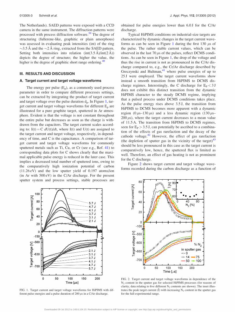
and target voltage over the pulse duration dp. In Figure 1, tar-
get current and target voltage waveforms for different Ep are
illustrated for a pure graphite target, sputtered in Ar atmos-
phere. Evident is that the voltage is not constant throughout
the entire pulse but decreases as soon as the charge is with-
drawn from the capacitors. The target current scales accord-
ing to: I(t)¼C dU(t)/dt, where I(t) and U(t) are assigned to
the target current and target voltage, respectively, in depend-
ency of time, and C is the capacitance. A comparison of tar-
get current and target voltage waveforms for commonly
sputtered metals such as Ti, Cu, or Cr (see e.g., Ref. 41) to
corresponding data plots for C shows clearly that the maxi-
mal applicable pulse energy is reduced in the later case. This
implies a decreased total number of sputtered ions, owing to
the comparatively high ionization potential of carbon
(11.26 eV) and the low sputter yield of 0.197 atoms/ion
(in Ar with 500 eV) in the C/Ar discharge. For the present
sputter system and process settings, stable processes are
obtained for pulse energies lower than 6.0 J for the C/Ar
discharge.
Typical HiPIMS conditions on industrial-size targets are
characterized by dynamic changes in the target current wave-
forms as can be seen in Figure 1 during the first 130 ls of
the pulse. The rather stable current values, which can be
observed in the last 70 ls of the pulses, reflect DCMS condi-
tions. As can be seen in Figure 1, the drop of the voltage and
thus the rise in current is not as pronounced in the C/Ar dis-
charge compared to, e.g., the Cr/Ar discharge described by
Greczynski and Hultman,41 where pulse energies of up to
25 J were employed. The target current waveforms show
instead a smooth transition from HiPIMS to DCMS dis-
charge regimes. Interestingly, the C discharge for EP< 3 J
does not exhibit this distinct transition from the dynamic
HiPIMS character to the steady DCMS regime, implying
that a pulsed process under DCMS conditions takes place.
As the pulse energy rises above 3.5 J, the transition from
HiPIMS to DCMS becomes more apparent with a dynamic
region (0 ls–130 ls) and a less dynamic region (130 ls–
200 ls), where the target current decreases to a mean value
of 11.5 A. The transition from HiPIMS to DCMS regimes,
seen for EP> 3.5 J, can potentially be ascribed to a combina-
tion of the effects of gas rarefaction and the decay of the
cathode voltage.42 However, the effect of gas rarefaction
(the depletion of sputter gas in the vicinity of the target)43
should be less pronounced in this case as the target current is
comparatively low, hence, the sputtered flux is limited as
well. Therefore, an effect of gas heating is not as prominent
for the C discharge.
Figure 2 shows target current and target voltage wave-
forms recorded during the carbon discharge as a function of
FIG. 1. Target current and target voltage waveforms for HiPIMS with dif-
ferent pulse energies and a pulse duration of 200 ls in a C/Ar discharge.
FIG. 2. Target current and target voltage waveforms in dependence of the
N2 content in the sputter gas for selected HiPIMS processes (for reasons of
clarity, data relating to five different N2 contents are shown). The inset illus-
trates the peak target current (I) with increasing N2 content in the sputter gas
for the full experimental range.
013305-3 Schmidt et al. J. Appl. Phys. 112, 013305 (2012)
Downloaded 09 Jul 2012 to 148.6.104.15. Redistribution subject to AIP license or copyright; see http://jap.aip.org/about/rights_and_permissions
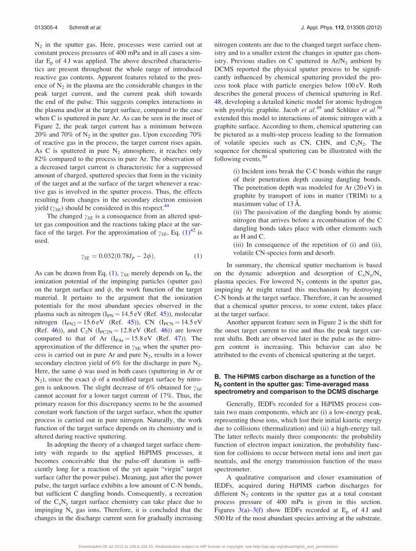
N2 in the sputter gas. Here, processes were carried out at
constant process pressures of 400 mPa and in all cases a sim-
ilar Ep of 4 J was applied. The above described characteris-
tics are present throughout the whole range of introduced
reactive gas contents. Apparent features related to the pres-
ence of N2 in the plasma are the considerable changes in the
peak target current, and the current peak shift towards
the end of the pulse. This suggests complex interactions in
the plasma and/or at the target surface, compared to the case
when C is sputtered in pure Ar. As can be seen in the inset of
Figure 2, the peak target current has a minimum between
20% and 70% of N2 in the sputter gas. Upon exceeding 70%
of reactive gas in the process, the target current rises again.
As C is sputtered in pure N2 atmosphere, it reaches only
82% compared to the process in pure Ar. The observation of
a decreased target current is characteristic for a suppressed
amount of charged, sputtered species that form in the vicinity
of the target and at the surface of the target whenever a reac-
tive gas is involved in the sputter process. Thus, the effects
resulting from changes in the secondary electron emission
yield (cSE) should be considered in this respect.44
The changed cSE is a consequence from an altered sput-
ter gas composition and the reactions taking place at the sur-
face of the target. For the approximation of cSE, Eq. (1)42 is
used.
cSE ¼ 0:032ð0:78IP � 2/Þ; (1)
As can be drawn from Eq. (1), cSE merely depends on IP, the
ionization potential of the impinging particles (sputter gas)
on the target surface and /, the work function of the target
material. It pertains to the argument that the ionization
potentials for the most abundant species observed in the
plasma such as nitrogen (IPN¼ 14.5 eV (Ref. 45)), molecular
nitrogen (IPN2¼ 15.6 eV (Ref. 45)), CN (IPCN¼ 14.5 eV
(Ref. 46)), and C2N (IPC2N¼ 12.8 eV (Ref. 46)) are lower
compared to that of Ar (IPAr¼ 15.8 eV (Ref. 47)). The
approximation of the difference in cSE when the sputter pro-
cess is carried out in pure Ar and pure N2, results in a lower
secondary electron yield of 6% for the discharge in pure N2.
Here, the same / was used in both cases (sputtering in Ar or
N2), since the exact / of a modified target surface by nitro-
gen is unknown. The slight decrease of 6% obtained for cSE
cannot account for a lower target current of 17%. Thus, the
primary reason for this discrepancy seems to be the assumed
constant work function of the target surface, when the sputter
process is carried out in pure nitrogen. Naturally, the work
function of the target surface depends on its chemistry and is
altered during reactive sputtering.
In adopting the theory of a changed target surface chem-
istry with regards to the applied HiPIMS processes, it
becomes conceivable that the pulse-off duration is suffi-
ciently long for a reaction of the yet again “virgin” target
surface (after the power pulse). Meaning, just after the power
pulse, the target surface exhibits a low amount of C-N bonds,
but sufficient C dangling bonds. Consequently, a recreation
of the CxNy target surface chemistry can take place due to
impinging Nx gas ions. Therefore, it is concluded that the
changes in the discharge current seen for gradually increasing
nitrogen contents are due to the changed target surface chem-
istry and to a smaller extent the changes in sputter gas chem-
istry. Previous studies on C sputtered in Ar/N2 ambient by
DCMS reported the physical sputter process to be signifi-
cantly influenced by chemical sputtering provided the pro-
cess took place with particle energies below 100 eV. Roth
describes the general process of chemical sputtering in Ref.
48, developing a detailed kinetic model for atomic hydrogen
with pyrolytic graphite. Jacob et al.49 and Schluter et al.50
extended this model to interactions of atomic nitrogen with a
graphite surface. According to them, chemical sputtering can
be pictured as a multi-step process leading to the formation
of volatile species such as CN, CHN, and C2N2. The
sequence for chemical sputtering can be illustrated with the
following events.50
(i) Incident ions break the C-C bonds within the range
of their penetration depth causing dangling bonds.
The penetration depth was modeled for Ar (20 eV) in
graphite by transport of ions in matter (TRIM) to a
maximum value of 13 A.
(ii) The passivation of the dangling bonds by atomic
nitrogen that arrives before a recombination of the C
dangling bonds takes place with other elements such
as H and C.
(iii) In consequence of the repetition of (i) and (ii),
volatile CN-species form and desorb.
In summary, the chemical sputter mechanism is based
on the dynamic adsorption and desorption of CxNy/Nx
plasma species. For lowered N2 contents in the sputter gas,
impinging Ar might retard this mechanism by destroying
C-N bonds at the target surface. Therefore, it can be assumed
that a chemical sputter process, to some extent, takes place
at the target surface.
Another apparent feature seen in Figure 2 is the shift for
the onset target current to rise and thus the peak target cur-
rent shifts. Both are observed later in the pulse as the nitro-
gen content is increasing. This behavior can also be
attributed to the events of chemical sputtering at the target.
B. The HiPIMS carbon discharge as a function of theN2 content in the sputter gas: Time-averaged massspectrometry and comparison to the DCMS discharge
Generally, IEDFs recorded for a HiPIMS process con-
tain two main components, which are (i) a low-energy peak,
representing those ions, which lost their initial kinetic energy
due to collisions (thermalization) and (ii) a high-energy tail.
The latter reflects mainly three components: the probability
function of electron impact ionization, the probability func-
tion for collisions to occur between metal ions and inert gas
neutrals, and the energy transmission function of the mass
spectrometer.
A qualitative comparison and closer examination of
IEDFs, acquired during HiPIMS carbon discharges for
different N2 contents in the sputter gas at a total constant
process pressure of 400 mPa is given in this section.
Figures 3(a)–3(f) show IEDFs recorded at Ep of 4 J and
500 Hz of the most abundant species arriving at the substrate.
013305-4 Schmidt et al. J. Appl. Phys. 112, 013305 (2012)
Downloaded 09 Jul 2012 to 148.6.104.15. Redistribution subject to AIP license or copyright; see http://jap.aip.org/about/rights_and_permissions
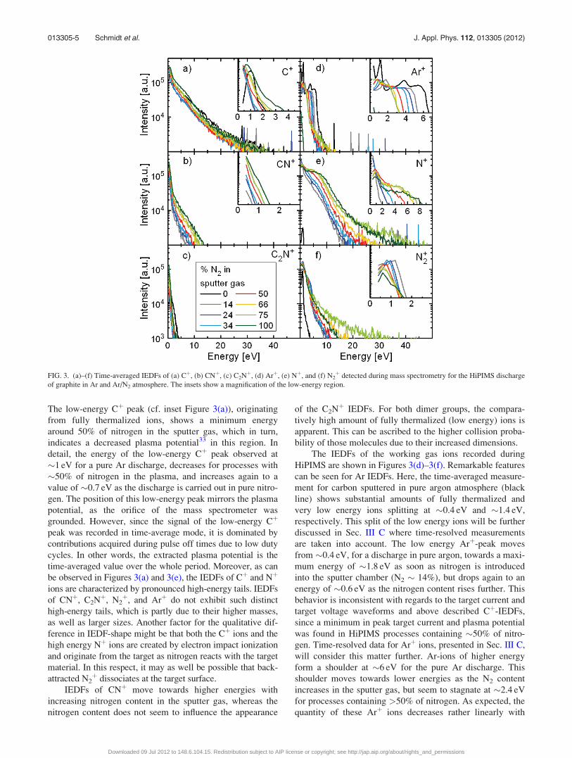
The low-energy Cþ peak (cf. inset Figure 3(a)), originating
from fully thermalized ions, shows a minimum energy
around 50% of nitrogen in the sputter gas, which in turn,
indicates a decreased plasma potential33 in this region. In
detail, the energy of the low-energy Cþ peak observed at
�1 eV for a pure Ar discharge, decreases for processes with
�50% of nitrogen in the plasma, and increases again to a
value of �0.7 eV as the discharge is carried out in pure nitro-
gen. The position of this low-energy peak mirrors the plasma
potential, as the orifice of the mass spectrometer was
grounded. However, since the signal of the low-energy Cþ
peak was recorded in time-average mode, it is dominated by
contributions acquired during pulse off times due to low duty
cycles. In other words, the extracted plasma potential is the
time-averaged value over the whole period. Moreover, as can
be observed in Figures 3(a) and 3(e), the IEDFs of Cþ and Nþ
ions are characterized by pronounced high-energy tails. IEDFs
of CNþ, C2Nþ, N2þ, and Arþ do not exhibit such distinct
high-energy tails, which is partly due to their higher masses,
as well as larger sizes. Another factor for the qualitative dif-
ference in IEDF-shape might be that both the Cþ ions and the
high energy Nþ ions are created by electron impact ionization
and originate from the target as nitrogen reacts with the target
material. In this respect, it may as well be possible that back-
attracted N2þ dissociates at the target surface.
IEDFs of CNþ move towards higher energies with
increasing nitrogen content in the sputter gas, whereas the
nitrogen content does not seem to influence the appearance
of the C2Nþ IEDFs. For both dimer groups, the compara-
tively high amount of fully thermalized (low energy) ions is
apparent. This can be ascribed to the higher collision proba-
bility of those molecules due to their increased dimensions.
The IEDFs of the working gas ions recorded during
HiPIMS are shown in Figures 3(d)–3(f). Remarkable features
can be seen for Ar IEDFs. Here, the time-averaged measure-
ment for carbon sputtered in pure argon atmosphere (black
line) shows substantial amounts of fully thermalized and
very low energy ions splitting at �0.4 eV and �1.4 eV,
respectively. This split of the low energy ions will be further
discussed in Sec. III C where time-resolved measurements
are taken into account. The low energy Arþ-peak moves
from �0.4 eV, for a discharge in pure argon, towards a maxi-
mum energy of �1.8 eV as soon as nitrogen is introduced
into the sputter chamber (N2 � 14%), but drops again to an
energy of �0.6 eV as the nitrogen content rises further. This
behavior is inconsistent with regards to the target current and
target voltage waveforms and above described Cþ-IEDFs,
since a minimum in peak target current and plasma potential
was found in HiPIMS processes containing �50% of nitro-
gen. Time-resolved data for Arþ ions, presented in Sec. III C,
will consider this matter further. Ar-ions of higher energy
form a shoulder at �6 eV for the pure Ar discharge. This
shoulder moves towards lower energies as the N2 content
increases in the sputter gas, but seem to stagnate at �2.4 eV
for processes containing >50% of nitrogen. As expected, the
quantity of these Arþ ions decreases rather linearly with
FIG. 3. (a)–(f) Time-averaged IEDFs of (a) Cþ, (b) CNþ, (c) C2Nþ, (d) Arþ, (e) Nþ, and (f) N2þ detected during mass spectrometry for the HiPIMS discharge
of graphite in Ar and Ar/N2 atmosphere. The insets show a magnification of the low-energy region.
013305-5 Schmidt et al. J. Appl. Phys. 112, 013305 (2012)
Downloaded 09 Jul 2012 to 148.6.104.15. Redistribution subject to AIP license or copyright; see http://jap.aip.org/about/rights_and_permissions
increasing nitrogen content up to 50%. A similar feature,
although at slightly higher energies (�7.6 eV for a process
carried out in pure nitrogen ambient), can also be observed
in IEDFs of Nþ.
Figures 3(e) and 3(f) present IEDFs for N2þ and Nþ as a
function of the nitrogen content in the sputter gas. As can be
seen, nitrogen ions dominate the discharge as soon as reac-
tive gas is introduced into the sputter chamber. Particularly,
the IEDFs for Nþ show, next to a minor low energy peak
originating from fully thermalized ions, a well-developed
shoulder of high-energy species. As discussed above, the
amount and energy of this portion of Nþ ions may only be
compared to that of Cþ. With increasing nitrogen content in
the sputter gas, the amount of the low-energy Nþ species
decreases, while the amount of higher energetic ions is
increasing. Moreover, the low-energy peak of Nþ ions shifts
to higher energy values for increasing nitrogen contents up
to 66% in the processes, simultaneously the low energy N2þ
peak is moving towards lower energies.
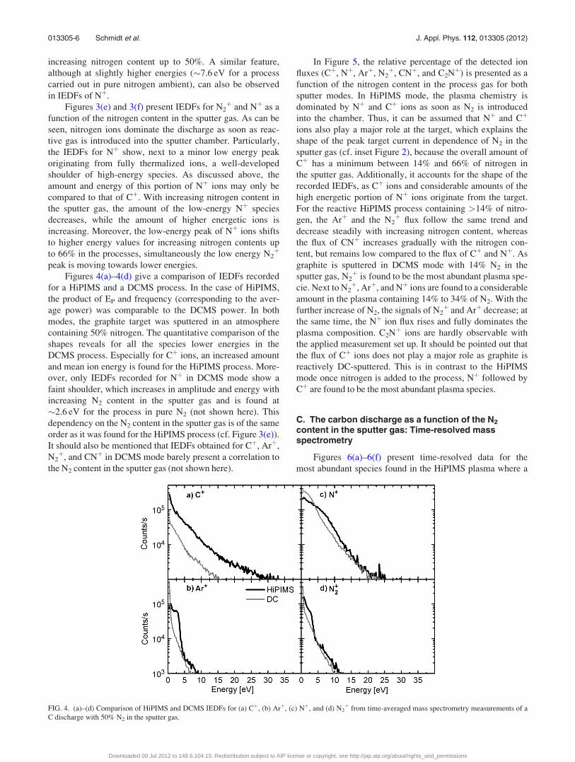
Figures 4(a)–4(d) give a comparison of IEDFs recorded
for a HiPIMS and a DCMS process. In the case of HiPIMS,
the product of EP and frequency (corresponding to the aver-
age power) was comparable to the DCMS power. In both
modes, the graphite target was sputtered in an atmosphere
containing 50% nitrogen. The quantitative comparison of the
shapes reveals for all the species lower energies in the
DCMS process. Especially for Cþ ions, an increased amount
and mean ion energy is found for the HiPIMS process. More-
over, only IEDFs recorded for Nþ in DCMS mode show a
faint shoulder, which increases in amplitude and energy with
increasing N2 content in the sputter gas and is found at
�2.6 eV for the process in pure N2 (not shown here). This
dependency on the N2 content in the sputter gas is of the same
order as it was found for the HiPIMS process (cf. Figure 3(e)).
It should also be mentioned that IEDFs obtained for Cþ, Arþ,
N2þ, and CNþ in DCMS mode barely present a correlation to
the N2 content in the sputter gas (not shown here).
In Figure 5, the relative percentage of the detected ion
fluxes (Cþ, Nþ, Arþ, N2þ, CNþ, and C2Nþ) is presented as a
function of the nitrogen content in the process gas for both
sputter modes. In HiPIMS mode, the plasma chemistry is
dominated by Nþ and Cþ ions as soon as N2 is introduced
into the chamber. Thus, it can be assumed that Nþ and Cþ
ions also play a major role at the target, which explains the
shape of the peak target current in dependence of N2 in the
sputter gas (cf. inset Figure 2), because the overall amount of
Cþ has a minimum between 14% and 66% of nitrogen in
the sputter gas. Additionally, it accounts for the shape of the
recorded IEDFs, as Cþ ions and considerable amounts of the
high energetic portion of Nþ ions originate from the target.
For the reactive HiPIMS process containing >14% of nitro-
gen, the Arþ and the N2þ flux follow the same trend and
decrease steadily with increasing nitrogen content, whereas
the flux of CNþ increases gradually with the nitrogen con-
tent, but remains low compared to the flux of Cþ and Nþ. As
graphite is sputtered in DCMS mode with 14% N2 in the
sputter gas, N2þ is found to be the most abundant plasma spe-
cie. Next to N2þ, Arþ, and Nþ ions are found to a considerable
amount in the plasma containing 14% to 34% of N2. With the
further increase of N2, the signals of N2þ and Arþ decrease; at
the same time, the Nþ ion flux rises and fully dominates the
plasma composition. C2Nþ ions are hardly observable with
the applied measurement set up. It should be pointed out that
the flux of Cþ ions does not play a major role as graphite is
reactively DC-sputtered. This is in contrast to the HiPIMS
mode once nitrogen is added to the process, Nþ followed by
Cþ are found to be the most abundant plasma species.
C. The carbon discharge as a function of the N2
content in the sputter gas: Time-resolved massspectrometry
Figures 6(a)–6(f) present time-resolved data for the
most abundant species found in the HiPIMS plasma where a
FIG. 4. (a)–(d) Comparison of HiPIMS and DCMS IEDFs for (a) Cþ, (b) Arþ, (c) Nþ, and (d) N2þ from time-averaged mass spectrometry measurements of a
C discharge with 50% N2 in the sputter gas.
013305-6 Schmidt et al. J. Appl. Phys. 112, 013305 (2012)
Downloaded 09 Jul 2012 to 148.6.104.15. Redistribution subject to AIP license or copyright; see http://jap.aip.org/about/rights_and_permissions
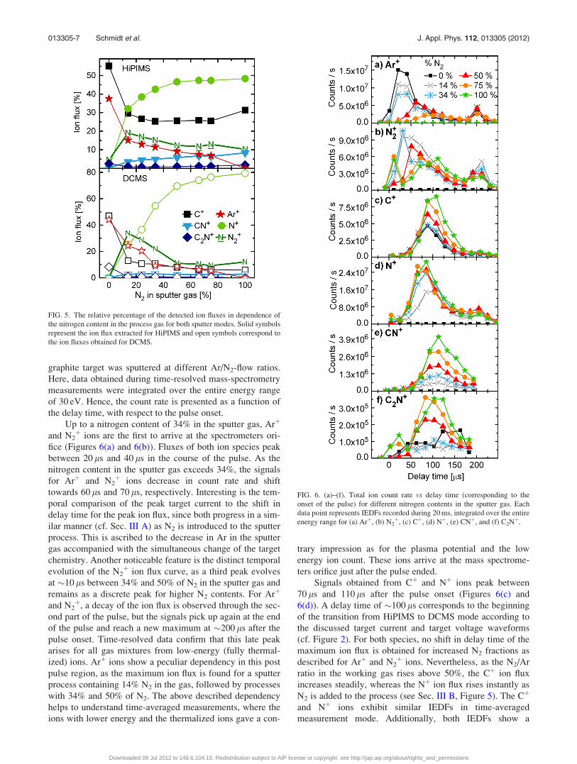
graphite target was sputtered at different Ar/N2-flow ratios.
Here, data obtained during time-resolved mass-spectrometry
measurements were integrated over the entire energy range
of 30 eV. Hence, the count rate is presented as a function of
the delay time, with respect to the pulse onset.
Up to a nitrogen content of 34% in the sputter gas, Arþ
and N2þ ions are the first to arrive at the spectrometers ori-
fice (Figures 6(a) and 6(b)). Fluxes of both ion species peak
between 20 ls and 40 ls in the course of the pulse. As the
nitrogen content in the sputter gas exceeds 34%, the signals
for Arþ and N2þ ions decrease in count rate and shift
towards 60 ls and 70 ls, respectively. Interesting is the tem-
poral comparison of the peak target current to the shift in
delay time for the peak ion flux, since both progress in a sim-
ilar manner (cf. Sec. III A) as N2 is introduced to the sputter
process. This is ascribed to the decrease in Ar in the sputter
gas accompanied with the simultaneous change of the target
chemistry. Another noticeable feature is the distinct temporal
evolution of the N2þ ion flux curve, as a third peak evolves
at �10 ls between 34% and 50% of N2 in the sputter gas and
remains as a discrete peak for higher N2 contents. For Arþ
and N2þ, a decay of the ion flux is observed through the sec-
ond part of the pulse, but the signals pick up again at the end
of the pulse and reach a new maximum at �200 ls after the
pulse onset. Time-resolved data confirm that this late peak
arises for all gas mixtures from low-energy (fully thermal-
ized) ions. Arþ ions show a peculiar dependency in this post
pulse region, as the maximum ion flux is found for a sputter
process containing 14% N2 in the gas, followed by processes
with 34% and 50% of N2. The above described dependency
helps to understand time-averaged measurements, where the
ions with lower energy and the thermalized ions gave a con-
trary impression as for the plasma potential and the low
energy ion count. These ions arrive at the mass spectrome-
ters orifice just after the pulse ended.
Signals obtained from Cþ and Nþ ions peak between
70 ls and 110 ls after the pulse onset (Figures 6(c) and
6(d)). A delay time of �100 ls corresponds to the beginning
of the transition from HiPIMS to DCMS mode according to
the discussed target current and target voltage waveforms
(cf. Figure 2). For both species, no shift in delay time of the
maximum ion flux is obtained for increased N2 fractions as
described for Arþ and N2þ ions. Nevertheless, as the N2/Ar
ratio in the working gas rises above 50%, the Cþ ion flux
increases steadily, whereas the Nþ ion flux rises instantly as
N2 is added to the process (see Sec. III B, Figure 5). The Cþ
and Nþ ions exhibit similar IEDFs in time-averaged
measurement mode. Additionally, both IEDFs show a
FIG. 6. (a)–(f). Total ion count rate vs delay time (corresponding to the
onset of the pulse) for different nitrogen contents in the sputter gas. Each
data point represents IEDFs recorded during 20 ms, integrated over the entire
energy range for (a) Arþ, (b) N2þ, (c) Cþ, (d) Nþ, (e) CNþ, and (f) C2Nþ.
FIG. 5. The relative percentage of the detected ion fluxes in dependence of
the nitrogen content in the process gas for both sputter modes. Solid symbols
represent the ion flux extracted for HiPIMS and open symbols correspond to
the ion fluxes obtained for DCMS.
013305-7 Schmidt et al. J. Appl. Phys. 112, 013305 (2012)
Downloaded 09 Jul 2012 to 148.6.104.15. Redistribution subject to AIP license or copyright; see http://jap.aip.org/about/rights_and_permissions
comparable temporal evolution in time-resolved measure-
ments. This supports the theory that not only Cþ is originat-
ing from the target but also a large portion of Nþ ions.
CNþ and C2Nþ ions show a maximum count rate at
�110 ls. While the CNþ ion flux is heavily scaling with the
N2 content in the working gas, the C2Nþ ion flux rises first
above the detection limit as N2 exceeds 50% in the sputter
gas. However, the overall count rates for C2Nþ and CNþ
ions are rather low, owing to the comparatively bulky mole-
cule dimensions and thus a higher collision probability in
combination with the large distance between the target sur-
face and the spectrometer’s orifice. Moreover, a shift in
delay time of the maximum ion flux is not observed for these
plasma species as N2 is added to the process. This points
towards the target as the origin of CNþ and C2Nþ, which is
supported by the theory of the chemical sputter process
occurring at the target surface.17,19,23,24
D. DCMS vs. HiPIMS processes; their impact on CNx
film growth and microstructure
Compared to the DCMS discharge, HiPIMS exhibits
most of all an increased amount of higher energy Cþ ions.
Arþ and Nþ, though comparable in abundance, were also
found to be more energetic, which in turn is accompanied by
a significantly decreased amount of thermalized ions in the
HiPIMS process (cf. Figure 4). The higher ion energy, the sig-
nificant differences in plasma composition (cf. Figure 5) and a
likely variation of the ion-to-neutral ratio imply influences on
the growth and microstructure in CNx thin films sputtered by
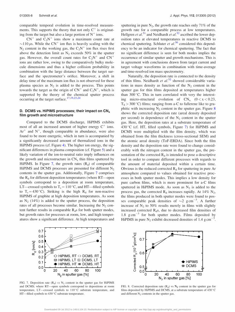
HiPIMS. In Figure 7, the growth rates (Rd) of comparable
HiPIMS and DCMS processes are presented for different N2
contents in the sputter gas. Additionally, Figure 7 comprises
the Rd for different deposition temperatures (where RT—open
symbols correspond to a deposition at room temperature,
LT—crossed symbols to Ts¼ 110 �C, and HT—filled symbols
to Ts¼ 430 �C). Striking is the high Rd for non-reactive
HiPIMS of graphite at high deposition temperatures. As soon
as N2 (14%) is added to the sputter process, the deposition
rates of all processes become similar. Increasing the N2 con-
tent further results in comparable Rds for both sputter modes,
but growth rates for processes at room, low, and high temper-
atures show a significant difference. At high temperatures and
sputtering in pure N2, the growth rate reaches only 71% of the
growth rate for a comparable process at low temperatures.
Hellgren et al.51 and Neidhardt et al.52 ascribed the lower dep-
osition rates at elevated temperatures in reactive DCMS to
chemical sputtering. Schluter et al.50 considered this depend-
ency to be an indicator for chemical sputtering. The fact that
no significant difference is seen for both modes implies the
occurrence of similar sputter and growth mechanisms. This is
in agreement with conclusions drawn from target current and
target voltage waveforms in combination with time-average
and time-resolved ion mass spectrometry.
Naturally, the deposition rate is connected to the density
of thin films. Neidhardt et al.52 showed considerable varia-
tions in mass density as function of the N2 content in the
sputter gas for thin films deposited at temperatures higher
than 300 �C. This in turn correlated with very the interest-
ing micro-structural evolution of CNx (0< x< 0.23,
TS> 300 �C) films; ranging from a-C to fullerene like to gra-
phitic with increasing N2 content in the sputter gas. Figure 8
shows the corrected deposition rate (areal density deposited
per second) in dependence of the N2 content in the sputter
gas. Here, the deposition rates at a substrate temperature of
430 �C (cf. HT, filled symbols, Figure 7) for HiPIMS and
DCMS were multiplied with the film density, which was
obtained from the film thickness (cross-sectional SEM) and
the atomic areal density (ToF-ERDA). Since both the film
density and the deposition rate were found to change consid-
erably with the nitrogen content in the sputter gas, the pre-
sentation of the corrected Rd is intended to pose a descriptive
tool in order to compare different processes with regards to
the amount of material deposited within a certain time.
Obvious is the reduced corrected Rd for sputtering in pure Ar
atmosphere compared to values obtained for reactive proc-
esses in both sputter modes. This implies a low density for
pure carbon films, which is more prominent for a-C films
sputtered in HiPIMS mode. As soon as N2 is added to the
process gas, the corrected Rd increases rapidly. At 14% N2,
the films produced in both sputter modes were found to pos-
ses comparable peak densities of �2 g cm�3. A further
increase of N2 to 50% results merely in films with slightly
increased corrected Rds, due to decreased film densities of
1.8 g cm�3 for both sputter modes. Films deposited by
HiPIMS in pure N2 exhibit decreased densities of 1.4 g cm�3.
FIG. 7. Deposition rate (Rd) vs N2 content in the sputter gas for HiPIMS
and DCMS; where RT—open symbols correspond to depositions at room
temperature, LT—crossed symbols to 110 �C substrate temperature, and
HT—filled symbols to 430 �C substrate temperature.
FIG. 8. Corrected deposition rate (Rd) vs N2 content in the sputter gas for
films deposited by HiPIMS and DCMS, at a substrate temperature of 430 �Cand different N2 contents in the sputter gas.
013305-8 Schmidt et al. J. Appl. Phys. 112, 013305 (2012)
Downloaded 09 Jul 2012 to 148.6.104.15. Redistribution subject to AIP license or copyright; see http://jap.aip.org/about/rights_and_permissions
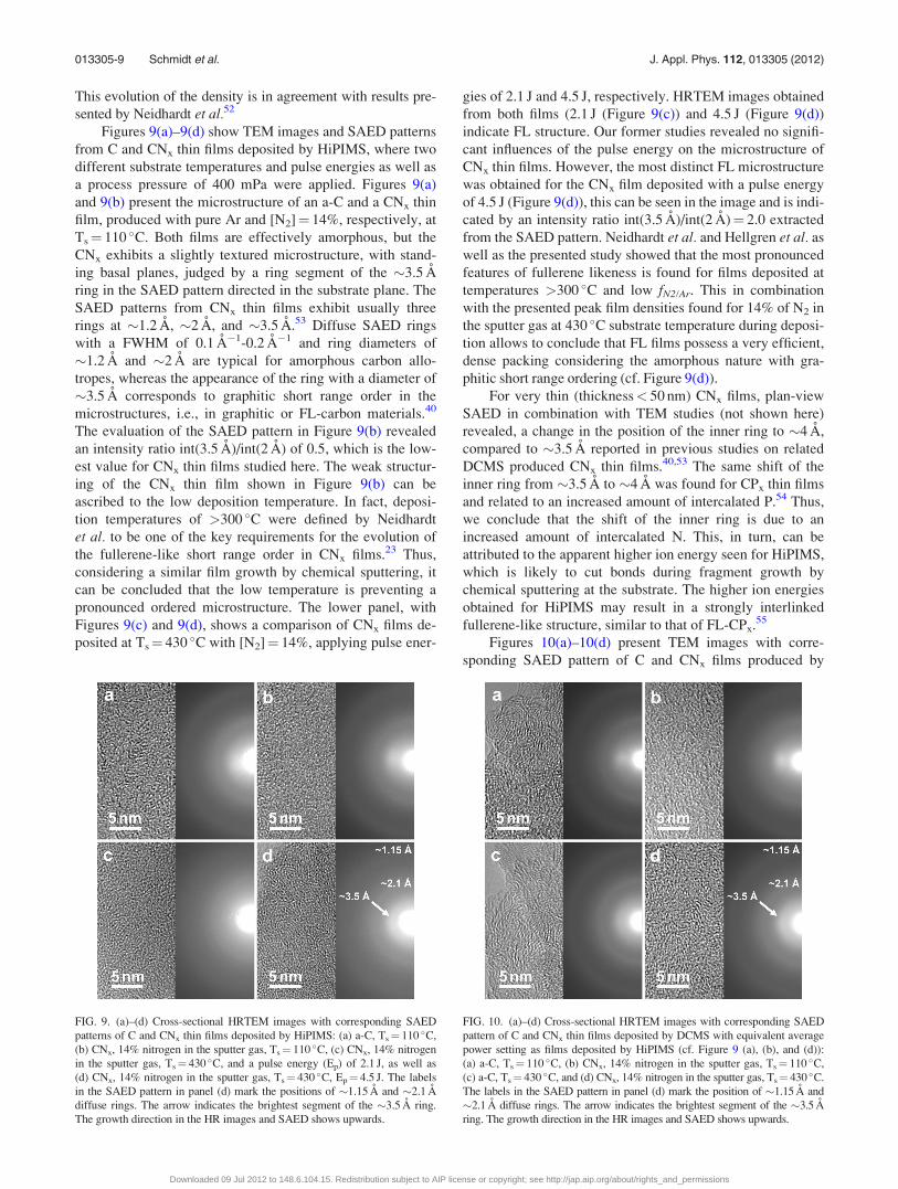
This evolution of the density is in agreement with results pre-
sented by Neidhardt et al.52
Figures 9(a)–9(d) show TEM images and SAED patterns
from C and CNx thin films deposited by HiPIMS, where two
different substrate temperatures and pulse energies as well as
a process pressure of 400 mPa were applied. Figures 9(a)
and 9(b) present the microstructure of an a-C and a CNx thin
film, produced with pure Ar and [N2]¼ 14%, respectively, at
Ts¼ 110 �C. Both films are effectively amorphous, but the
CNx exhibits a slightly textured microstructure, with stand-
ing basal planes, judged by a ring segment of the �3.5 A
ring in the SAED pattern directed in the substrate plane. The
SAED patterns from CNx thin films exhibit usually three
rings at �1.2 A, �2 A, and �3.5 A.53 Diffuse SAED rings
with a FWHM of 0.1 A�1-0.2 A�1 and ring diameters of
�1.2 A and �2 A are typical for amorphous carbon allo-
tropes, whereas the appearance of the ring with a diameter of
�3.5 A corresponds to graphitic short range order in the
microstructures, i.e., in graphitic or FL-carbon materials.40
The evaluation of the SAED pattern in Figure 9(b) revealed
an intensity ratio int(3.5 A)/int(2 A) of 0.5, which is the low-
est value for CNx thin films studied here. The weak structur-
ing of the CNx thin film shown in Figure 9(b) can be
ascribed to the low deposition temperature. In fact, deposi-
tion temperatures of >300 �C were defined by Neidhardt
et al. to be one of the key requirements for the evolution of
the fullerene-like short range order in CNx films.23 Thus,
considering a similar film growth by chemical sputtering, it
can be concluded that the low temperature is preventing a
pronounced ordered microstructure. The lower panel, with
Figures 9(c) and 9(d), shows a comparison of CNx films de-
posited at Ts¼ 430 �C with [N2]¼ 14%, applying pulse ener-
gies of 2.1 J and 4.5 J, respectively. HRTEM images obtained
from both films (2.1 J (Figure 9(c)) and 4.5 J (Figure 9(d))
indicate FL structure. Our former studies revealed no signifi-
cant influences of the pulse energy on the microstructure of
CNx thin films. However, the most distinct FL microstructure
was obtained for the CNx film deposited with a pulse energy
of 4.5 J (Figure 9(d)), this can be seen in the image and is indi-
cated by an intensity ratio int(3.5 A)/int(2 A)¼ 2.0 extracted
from the SAED pattern. Neidhardt et al. and Hellgren et al. as
well as the presented study showed that the most pronounced
features of fullerene likeness is found for films deposited at
temperatures >300 �C and low fN2/Ar. This in combination
with the presented peak film densities found for 14% of N2 in
the sputter gas at 430 �C substrate temperature during deposi-
tion allows to conclude that FL films possess a very efficient,
dense packing considering the amorphous nature with gra-
phitic short range ordering (cf. Figure 9(d)).
For very thin (thickness< 50 nm) CNx films, plan-view
SAED in combination with TEM studies (not shown here)
revealed, a change in the position of the inner ring to �4 A,
compared to �3.5 A reported in previous studies on related
DCMS produced CNx thin films.40,53 The same shift of the
inner ring from �3.5 A to �4 A was found for CPx thin films
and related to an increased amount of intercalated P.54 Thus,
we conclude that the shift of the inner ring is due to an
increased amount of intercalated N. This, in turn, can be
attributed to the apparent higher ion energy seen for HiPIMS,
which is likely to cut bonds during fragment growth by
chemical sputtering at the substrate. The higher ion energies
obtained for HiPIMS may result in a strongly interlinked
fullerene-like structure, similar to that of FL-CPx.55
Figures 10(a)–10(d) present TEM images with corre-
sponding SAED pattern of C and CNx films produced by
FIG. 9. (a)–(d) Cross-sectional HRTEM images with corresponding SAED
patterns of C and CNx thin films deposited by HiPIMS: (a) a-C, Ts¼ 110 �C,
(b) CNx, 14% nitrogen in the sputter gas, Ts¼ 110 �C, (c) CNx, 14% nitrogen
in the sputter gas, Ts¼ 430 �C, and a pulse energy (Ep) of 2.1 J, as well as
(d) CNx, 14% nitrogen in the sputter gas, Ts¼ 430 �C, Ep¼ 4.5 J. The labels
in the SAED pattern in panel (d) mark the positions of �1.15 A and �2.1 A
diffuse rings. The arrow indicates the brightest segment of the �3.5 A ring.
The growth direction in the HR images and SAED shows upwards.
FIG. 10. (a)–(d) Cross-sectional HRTEM images with corresponding SAED
pattern of C and CNx thin films deposited by DCMS with equivalent average
power setting as films deposited by HiPIMS (cf. Figure 9 (a), (b), and (d)):
(a) a-C, Ts¼ 110 �C, (b) CNx, 14% nitrogen in the sputter gas, Ts¼ 110 �C,
(c) a-C, Ts¼ 430 �C, and (d) CNx, 14% nitrogen in the sputter gas, Ts¼ 430 �C.
The labels in the SAED pattern in panel (d) mark the position of �1.15 A and
�2.1 A diffuse rings. The arrow indicates the brightest segment of the �3.5 A
ring. The growth direction in the HR images and SAED shows upwards.
013305-9 Schmidt et al. J. Appl. Phys. 112, 013305 (2012)
Downloaded 09 Jul 2012 to 148.6.104.15. Redistribution subject to AIP license or copyright; see http://jap.aip.org/about/rights_and_permissions
DCMS. Figures 10(a) and 10(c) show films sputtered from a
graphite target in pure Ar at 110 �C and 430 �C, respectively.
The SAED patterns of both a-C films show a slight graphitic
ordering with ring intensity ratios of 0.5. DCMS sputtered
CNx films at temperatures of 110 �C (Figure 10(b)) and
430 �C (Figure 10(d)) were evaluated to ratios of 0.7 and 1.3,
respectively. The bright segment of the �3.5 A ring implies
a slightly textured graphitic ordering of the CNx film (with
preferred orientation of basal planes perpendicular to the
substrate) seen in Figure 10(d). The comparison of TEM
images and SAED patterns for HiPIMS CNx thin films and
DCMS CNx thin films presented in this study reveals that the
degree of ordering is highest for the HiPIMS CNx thin film
sputtered in nitrogen containing atmosphere at Ts¼ 430 �C.
Thus, it can be concluded that the structure-defining impact of
chemical sputtering during CNx film growth is particularly
effective in the HiPIMS process. This is evident from ion mass
spectrometry, as more CxNy (x, y� 2) ionic species, acting as
structure-defining agents at the substrate, were found for the
HiPIMS mode compared to DCMS (cf. Figure 5). However,
high-energy particles may counteract the evolution of highly
ordered microstructures in films deposited by HiPIMS.
IV. CONCLUSIONS
Reactive DCMS and HiPIMS of graphite in an Ar/N2
atmosphere yield a discharge that contains mainly Cþ, Nþ,
N2þ, as well as Arþ and to a lower extent CNþ and C2Nþ ions.
The ion species in HiPIMS processes exhibit higher ion ener-
gies and a lower amount of fully thermalized ions compared
to DCMS. With regards to ion energy and amount, Cþ ions
exhibit distinct differences, with two and four orders of
magnitude higher values, respectively, obtained for HiPIMS
processing. Once nitrogen is added to the sputter process,
Nþ-ions dominate the plasma chemistry. This effect is far less
pronounced in the case of HiPIMS as the ion-flux at 50% of
nitrogen in the process gas is composed of 26% Cþ and 47%
Nþ in contrast to the DCMS plasma, which contains 8% of Cþ
and 70% of Nþ at equivalent process settings. The comparison
on the ion-flux shows further a rising amount of CxNy (x, y� 2)
species in the HiPIMS plasma. This in combination with the
conclusions drawn from the evaluation of the target current
confirms that chemical sputtering is active at the substrate and
at target as soon as nitrogen is added to the sputter process.
The most pronounced FL structure is obtained for CNx films
sputtered in HiPIMS mode at 430 �C. Pure carbon thin films as
well as CNx thin films deposited at low substrate temperatures of
110 �C exhibit only slight graphitic short range ordering. In the
case of HiPIMS, the increased amount of pre-formed ionic CxNy
(x, y� 2) species by chemical sputtering at high temperatures
promotes the formation of FL-CNx. The comparatively high
energies detected for Nþ and Cþ ions in the HiPIMS process dis-
turb the FL structure by intercalation of N in the films.
ACKNOWLEDGMENTS
The VINN Excellence Center Functional NanoscaleMaterials (FunMat) is acknowleged. We are thankful for the
access to the Tandem Laboratory, Uppsala University. Zsolt
Czigany acknowledges the Bolyai Scholarship of the
Hungarian Academy of Sciences.
1J. Robertson, Adv. Phys. 35, 317–374 (1986).2J. Robertson, Pure Appl. Chem. 66, 1789–1796 (1994).3Y. Lifshitz, Diamond Relat. Mater. 5, 388–400 (1996).4Y. Lifshitz, Diamond Relat. Mater. 8, 1659–1676 (1999).5J. Robertson, Mater. Sci. Eng. R 37, 129–281 (2002).6J. Robertson, Prog. Solid State Chem. 21, 199–333 (1991).7J. Robertson, Surf. Coat. Technol. 50, 185–203 (1992).8J. Robertson, Thin Solid Films 383, 81–88 (2001).9A. A. Voevodin, C. Rebholz, J. M. Schneider, P. Stevenson, and A.
Matthews, Surf. Coat. Technol. 73, 185–197 (1995).10T. Mikami, H. Nakazawa, M. Kudo, and M. Mashita, Thin Solid Films
488, 87–92 (2005).11C. A. Davis, G. A. J. Amaratunga, and K. M. Knowles, Phys. Rev. Lett.
80, 3280–3283 (1998).12J. C. Angus and C. C. Hayman, Science 241, 913–921 (1988).13J. Robertson, Phys. Rev. Lett. 68, 220–223 (1992).14A. Grill, Diamond Relat. Mater. 12, 166–170 (2003).15S. S. Tinchev, Y. Dyulgerska, P. Nikolova, D. Grambole, U. Kreissig, and
T. Z. Babeva, J. Optoelectron. Adv. Mater. 8, 308–311 (2006).16C. Casiraghi, J. Robertson, and A. C. Ferrari, Mater. Today 10, 44–53
(2007).17N. Hellgren, K. Macak, E. Broitman, M. P. Johansson, L. Hultman, and
J. E. Sundgren, J. Appl. Phys. 88, 524–532 (2000).18B. Kleinsorge, A. C. Ferrari, J. Robertson, W. I. Milne, S. Waidmann, and
S. Hearne, Diamond Relat. Mater. 9, 643–648 (2000).19J. Neidhardt, L. Hultman, E. Broitman, T. W. Scharf, and I. L. Singer,
Diamond Relat. Mater. 13, 1882–1888 (2004).20G. Abrasonis, R. Gago, M. Vinnichenko, U. Kreissig, A. Kolitsch, and
W. Moller, Phys. Rev. B 73, 13 (2006).21R. Kaltofen, T. Sebald, and G. Weise, in Plasma Diagnostic Studies to the
Carbon Nitride Film Deposition by Reactive Rf Magnetron Sputtering(Elsevier Science Sa Lausanne, 1996), pp. 112–119.
22S. E. Rodil and S. Muhl, Diamond Relat. Mater. 13, 1521–1531 (2004).23J. Neidhardt, Z. Czigany, I. F. Brunell, and L. Hultman, J. Appl. Phys. 93,
3002–3015 (2003).24L. Hultman, J. Neidhardt, N. Hellgren, H. Sjostrom, and J. E. Sundgren,
MRS Bull. 28, 194–202 (2003).25V. Kouznetsov, K. Macak, J. M. Schneider, U. Helmersson, and I. Petrov,
Surf. Coat. Technol. 122, 290–293 (1999).26J. Bohlmark, M. Ostbye, M. Lattemann, H. Ljungcrantz, T. Rosell, and
U. Helmersson, Thin Solid Films 515, 1928–1931 (2006).27A. P. Ehiasarian, R. New, W. D. Munz, L. Hultman, U. Helmersson, and
V. Kouznetsov, in Influence of High Power Densities on the Compositionof Pulsed Magnetron Plasmas (Pergamon, 2002), pp. 147–154.
28J. T. Gudmundsson, J. Alami, and U. Helmersson, Surf. Coat. Technol.
161, 249–256 (2002).29A. P. Ehiasarian, W. D. Munz, L. Hultman, U. Helmersson, and I. Petrov,
Surf. Coat. Technol. 163, 267–272 (2003).30G. Hakansson, L. Hultman, J. E. Sundgren, J. E. Greene, and W. D. Munz,
Surf. Coat. Technol. 48, 51–67 (1991).31I. Petrov, F. Adibi, J. E. Greene, L. Hultman, and J. E. Sundgren, Appl.
Phys. Lett. 63, 36–38 (1993).32B. M. DeKoven, P. R. Ward, R. E. Weiss, D. J. Christie, R. A. Scholl,
W. D. Sproul, F. Tomasel, and A. Anders, in Carbon Thin Film DepositionUsing High Power Pulsed Magnetron Sputtering (2003), pp. 158–165.
33A. Hecimovic, K. Burcalova, and A. P. Ehiasarian, J. Phys. D: Appl. Phys.
41, 10 (2008).34A. Hecimovic and A. P. Ehiasarian, IEEE Trans. Plasma Sci. 39,
1154–1164 (2011).35J. Bohlmark, M. Lattemann, J. T. Gudmundsson, A. P. Ehiasarian, Y. A.
Gonzalvo, N. Brenning, and U. Helmersson, Thin Solid Films 515,
1522–1526 (2006).36H. J. Whitlow, G. Possnert, and C. S. Petersson, Nucl. Instrum. Methods
Phys. Res. B 27, 448–457 (1987).37J. Jensen, D. Martin, A. Surpi, and T. Kubart, Nucl. Instrum. Methods
Phys. Res. B 268, 1893–1898 (2010).38J. P. McCaffrey, Microsc. Res. Tech. 24, 180–184 (1993).39J. L. Labar, Microsc. Microanal. 15, 20–29 (2009).40Z. Czigany and L. Hultman, Ultramicroscopy 110, 815–819 (2010).41G. Greczynski and L. Hultman, Vacuum 84, 1159–1170 (2010).
013305-10 Schmidt et al. J. Appl. Phys. 112, 013305 (2012)
Downloaded 09 Jul 2012 to 148.6.104.15. Redistribution subject to AIP license or copyright; see http://jap.aip.org/about/rights_and_permissions

42A. Anders, Surf. Coat. Technol. 205, S1–S9 (2011).43S. M. Rossnagel, J. Vac. Sci. Technol. A 6, 19–24 (1988).44N. Hellgren, M. P. Johansson, E. Broitman, L. Hultman, and J.-E. Sundgren,
Phys. Rev. B 59, 5162 (1999).45E. P. L. Hunter and S. G. Lias, J. Phys. Chem. Ref. Data 27, 413–656
(1998).46V. H. Dibeler, R. M. Reese, and J. L. Franklin, J. Am. Chem. Soc. 83,
1813–1818 (1961).47R. C. Wetzel, F. A. Baiocchi, T. R. Hayes, and R. S. Freund, Phys. Rev. A
35, 559–577 (1987).48J. Roth, “Chemical sputtering,” in Sputtering by Particle Bombardment II,
edited by R. Behrisch (Springer, Berlin Heidelberg, 1983), Chap. 3.5,
pp. 116–146.
49W. Jacob, C. Hopf, and M. Schluter, Appl. Phys. Lett. 86, 204103
(2005).50M. Schlueter, C. Hopf, and W. Jacob, New J. Phys. 10, 17 (2008).51Hellgren, M. P. Johansson, E. Broitman, P. Sandstrom, L. Hultman, and J.
E. Sundgren, Thin Solid Films 382, 146–152 (2001).52J. Neidhardt, H. Hogberg, and L. Hultman, Thin Solid Films 478, 34–41
(2005).53J. Neidhardt, L. Hultman, and Z. Czigany, Carbon 42, 2729–2734
(2004).54G. K. Gueorguiev, Z. Czigany, A. Furlan, S. Stafstrom, and L. Hultman,
Chem. Phys. Lett. 501, 400–403 (2011).55G. K. Gueorguiev, A. Furlan, H. Hogberg, S. Stafstrom, and L. Hultman,
Chem. Phys. Lett. 426, 374–379 (2006).
013305-11 Schmidt et al. J. Appl. Phys. 112, 013305 (2012)
Downloaded 09 Jul 2012 to 148.6.104.15. Redistribution subject to AIP license or copyright; see http://jap.aip.org/about/rights_and_permissions