Embed Size (px)
Citation preview
UGIM 2016
Research Service CentersHerbert Wertheim College of Engineering
1
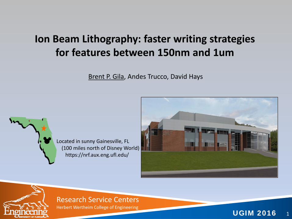
Ion Beam Lithography: faster writing strategies for features between 150nm and 1um
Brent P. Gila, Andes Trucco, David Hays
Located in sunny Gainesville, FL (100 miles north of Disney World)
https://nrf.aux.eng.ufl.edu/

UGIM 2016
Research Service CentersHerbert Wertheim College of Engineering
2
Patterning strategies are to separate features based upon size to minimize exposure time.
Lithography processing gap:
Affordable lithographic processes for average university facilities are contact aligners (and projection aligners) and SEM pattern generator attachments. These cover >1um and <1um respectively. Optical exposures are parallel and fast, electron beam exposures are serial and slow.
Ion beam lithography can provide gap coverage between the 200nm and 1um feature range. This is a serial process like electron beam lithography. However the ion exposure required for the resists are 10 times lower, so the writing time is greatly reduced compared to electron beam lithography.
Ion beam lithography overview
UGIM 2016
Research Service CentersHerbert Wertheim College of Engineering
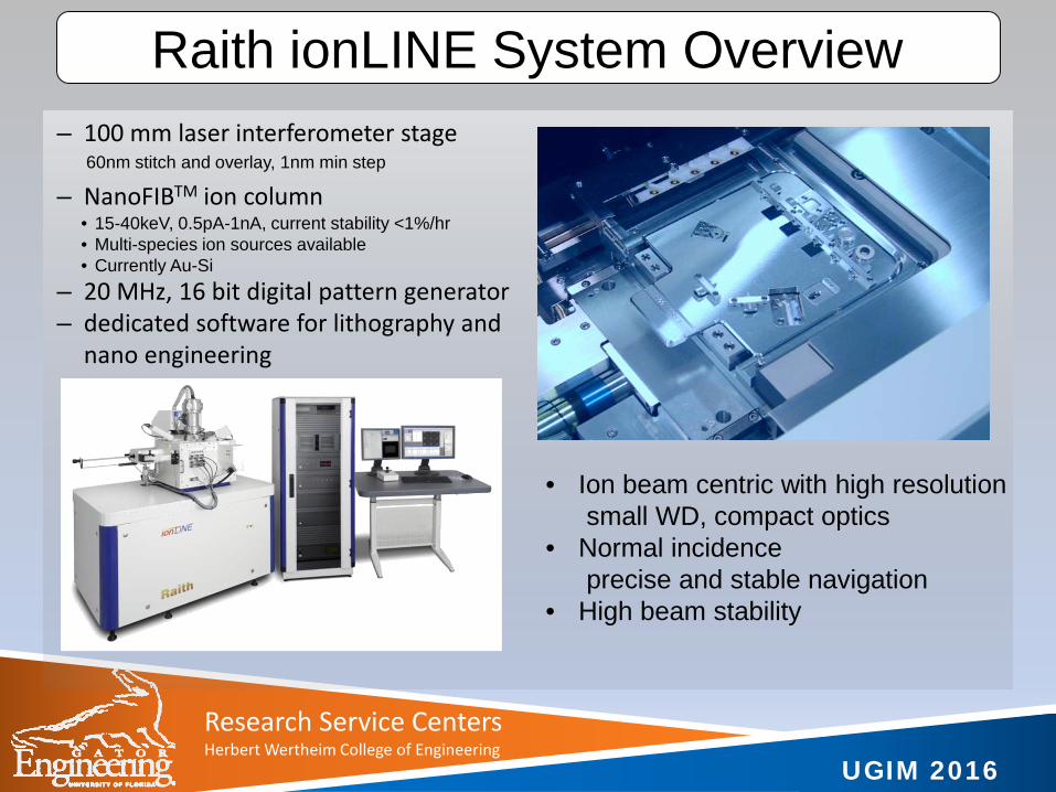
– 100 mm laser interferometer stage
– NanoFIBTM ion column
– 20 MHz, 16 bit digital pattern generator– dedicated software for lithography and
nano engineering
• Ion beam centric with high resolutionsmall WD, compact optics
• Normal incidenceprecise and stable navigation
• High beam stability
Raith ionLINE System Overview
• 15-40keV, 0.5pA-1nA, current stability <1%/hr• Multi-species ion sources available• Currently Au-Si
60nm stitch and overlay, 1nm min step
UGIM 2016
Research Service CentersHerbert Wertheim College of Engineering
4
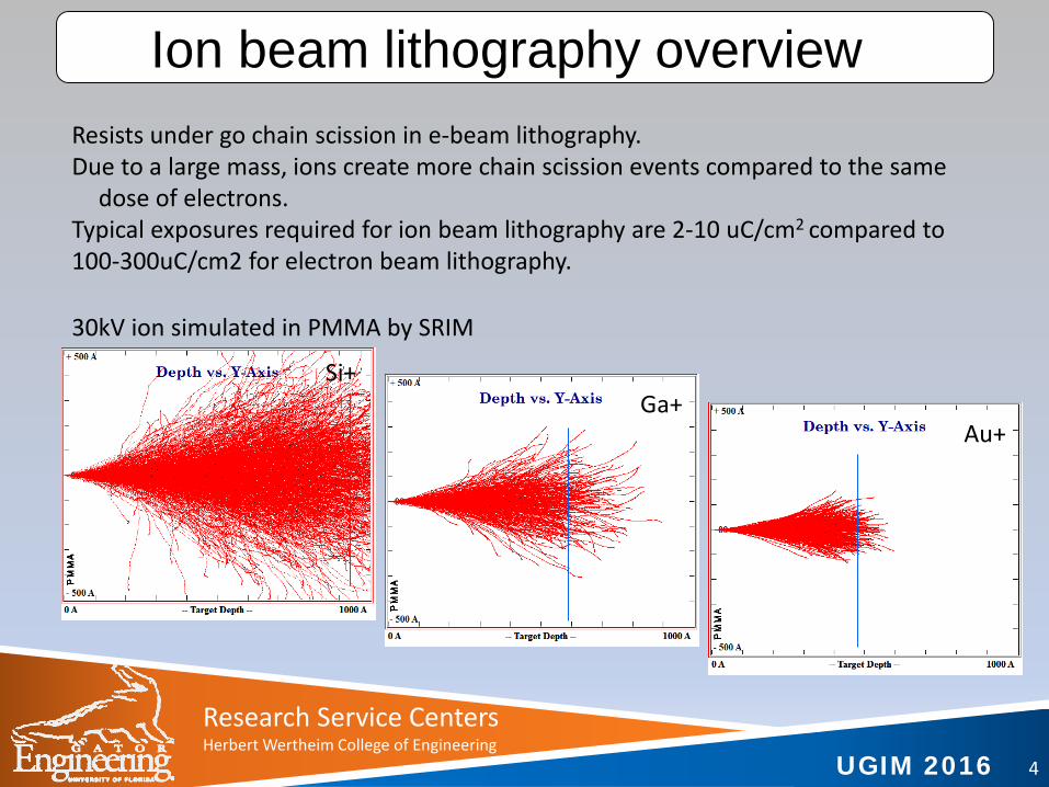
Ion beam lithography overview
Ga+Au+
30kV ion simulated in PMMA by SRIM
Si+
Resists under go chain scission in e-beam lithography.Due to a large mass, ions create more chain scission events compared to the same
dose of electrons.Typical exposures required for ion beam lithography are 2-10 uC/cm2 compared to 100-300uC/cm2 for electron beam lithography.

UGIM 2016
Research Service CentersHerbert Wertheim College of Engineering
5
Ion beam lithography overview
Si+ ion simulated in PMMA by SRIM
Depth of resist exposure is dependent upon ion kV, but high kV does not lead to higher aspect ratio structures, only deeper exposures for thicker resists. Ion scattering in PMMA remains large.
20kV
30kV
40kV
100nm resist
UGIM 2016
Research Service CentersHerbert Wertheim College of Engineering
6
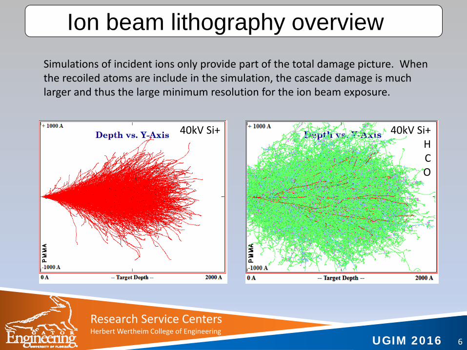
Ion beam lithography overviewSimulations of incident ions only provide part of the total damage picture. When the recoiled atoms are include in the simulation, the cascade damage is much larger and thus the large minimum resolution for the ion beam exposure.
40kV Si+ 40kV Si+HCO

UGIM 2016
Research Service CentersHerbert Wertheim College of Engineering
7
Ion beam lithography overview
Si ion beam exposure in 300nm PMMA has the same profile as the simulation.
To ensure proper clearing dose and not implant/damage the substrate, must us a sacrificial stopping layer under the PMMA.
Typical stopping layer employed is 200nm LOR.

UGIM 2016
Research Service CentersHerbert Wertheim College of Engineering
1.0mm/sec
0.1mm/sec 0.25mm/sec
Ga+ FBMS PMMA resist exposures
Patterning 50um PMMA over 300nm LOR with 6pA Ga+ 30kV,
Increasing stage speed to lower exposure dose.Very easy to overexpose and crosslink.
0.5mm/sec

UGIM 2016
Research Service CentersHerbert Wertheim College of Engineering
9
Si+ dose PMMA resist exposures40kV, 2uC/cm2, 100nm PMMA on 200nm LOR
200nm design 400nm design 600nm design
800nm design 1000nm design

UGIM 2016
Research Service CentersHerbert Wertheim College of Engineering
10
2uC/cm2 4uC/cm2 6uC/cm2
8uC/cm2 10uC/cm2 15uC/cm2
Si+ area dose PMMA resist exposures

UGIM 2016
Research Service CentersHerbert Wertheim College of Engineering
11
Si+ area dose PMMA resist exposuresOver exposures to PMMA do not lead to milling, but severe crosslinking.
65uC/cm2 70uC/cm2

UGIM 2016
Research Service CentersHerbert Wertheim College of Engineering
12
Au+ area dose PMMA resist exposures
10uC/cm2
8uC/cm26uC/cm24uC/cm2
20uC/cm2
Onset of PMMA crosslinking noticed at 6uC/cm2.
Complete crosslinking at 20uC/cm2.
UGIM 2016
Research Service CentersHerbert Wertheim College of Engineering
13
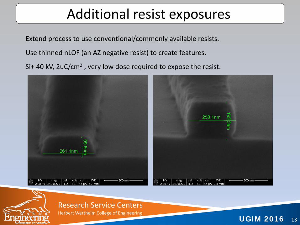
Additional resist exposuresExtend process to use conventional/commonly available resists.
Use thinned nLOF (an AZ negative resist) to create features.
Si+ 40 kV, 2uC/cm2 , very low dose required to expose the resist.
UGIM 2016
Research Service CentersHerbert Wertheim College of Engineering
14
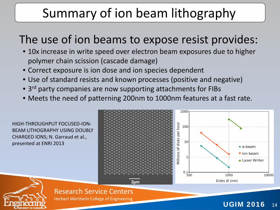
Summary of ion beam lithography
The use of ion beams to expose resist provides:• 10x increase in write speed over electron beam exposures due to higher
polymer chain scission (cascade damage)• Correct exposure is ion dose and ion species dependent• Use of standard resists and known processes (positive and negative)• 3rd party companies are now supporting attachments for FIBs• Meets the need of patterning 200nm to 1000nm features at a fast rate.
HIGH-THROUGHPUT FOCUSED-ION-BEAM LITHOGRAPHY USING DOUBLY CHARGED IONS; N. Garraud et al., presented at ENRI 2013