Embed Size (px)
Citation preview
INV ITEDP A P E R
Field-ProgrammableWiring SystemsThis paper discusses concepts of adaptive wiring manifolds, in which soft-configured
wires can be formed ‘‘on demand’’ to form dedicated conductive pathways that can
connect many points within an embedded system.
By Victor Murray, Senior Member IEEE, Marios Pattichis, Senior Member IEEE,
Daniel Llamocca, Senior Member IEEE, and James Lyke, Senior Member IEEE
ABSTRACT | Field-programmable wiring systems refer to
methods and hardware that can maintain the interconnection
of components of different types. Generally, field-programma-
ble wiring systems support the use of multidomain fabrics that
can be used to route analog, power, digital signals, optical,
microwave signals, etc. This paper reviews fundamental con-
cepts associated with the practical implementation of field-
programmable wiring systems. The paper also provides
different implementation examples and discusses a list of chal-
lenges and recommendations for future work in this area.
KEYWORDS | Adaptive wiring panel (AWP); field-programmable
wiring systems; reconfigurable manifold; self-healing circuits
I . INTRODUCTION
Field-programmable wiring systems are structures capable
of forming programmable interconnections between theterminals of components that are attached to these struc-
tures, along with the methodologies and tools for manag-
ing these interconnections. Some type of programmable
wiring concept will be at the heart of most reconfigurable
system approaches. The termini of black boxes, fixed and
configurable, that comprise such systems, must be inter-
connected, and programmable wiring approaches provide
additional flexibility and can enhance the expressive capa-
city of components that would otherwise be united with amanifold of fixed connections. In fact, one methodology
for creating a reconfigurable system involves flexibly con-
necting an arrangement of fixed components. In general,
the interconnections making up systems can be fixed,
programmable, dynamically reconfigurable, or based on a
combination of these concepts.
The most well-known example of a programmable wir-
ing system is the field-programmable gate array (FPGA)[1], [2]. FPGAs require programmable wiring to connect
together configurable logic elements, internal memories,
and other internally embedded intellectual property (IP)
blocks in support of an overall personalization. In the
1990s, some dedicated field-programmable interconnect
devices (FPIDs) were introduced into the marketplace [3],
[4], but they were eventually discontinued. These devices
were similar to FPGAs in that they used similar mecha-nisms for switching, routing, and configuration manage-
ment, but they only provided interconnection routing
functionality (i.e., no logic or memory resources).
FPGAs and FPIDs have traditionally been designed
around digital applications. It is, for example, straightfor-
ward to use an FPGA to connect together two digital de-
vices, and a wide range of interface styles (serial, parallel),
signaling standards, and physical layer types are supported.It is not, however, generally possible to connect a lightbulb
to a battery using an FPGA to program a wiring path be-
tween them. Not only are the voltage and current levels
incompatible, but sometimes the signals that are routed
through an FPGA are destroyed, manipulated, and regene-
rated as part of the routing process, which is sometimes
performed as a computation. Hence, using FPGAs for
general-purpose wiring chores is impractical.We believe the need for a more versatile adaptive wiring
approach will become more acute in the future as a broader
range of reconfigurable systems ideas are advanced. The
Manuscript received February 2, 2015; revised April 28, 2015; accepted May 8, 2015.
Date of publication June 1, 2015; date of current version June 18, 2015.
V. Murray is with the Department of Electrical Engineering, Universidad de Ingenieria
y Tecnologia, 2221 Lima, Peru, and also with the Department of Electrical and
Computer Engineering, University of New Mexico, Albuquerque, NM 87131 USA
(e-mail: [email protected]).
M. Pattichis is with the Department of Electrical and Computer Engineering, University
of New Mexico, Albuquerque, NM 87131 USA (e-mail: [email protected]).
D. Llamocca is with the Electrical and Computer Engineering Department, Oakland
University, Rochester, MI 48309 USA (e-mail: [email protected]).
J. Lyke is with the Space Vehicles Directorate, Air Force Research Laboratory,
Albuquerque, NM 87117 USA (e-mail: [email protected]).
Digital Object Identifier: 10.1109/JPROC.2015.2432123
0018-9219 � 2015 IEEE. Personal use is permitted, but republication/redistribution requires IEEE permission.See http://www.ieee.org/publications_standards/publications/rights/index.html for more information.
Vol. 103, No. 7, July 2015 | Proceedings of the IEEE 1159

authors have been involved in several projects spanningnearly two decades in pursuit of effective programmable
wiring technologies for general applications, to include
both the switch mechanisms themselves as well as fabrics
employing them. The work culminated in the development
of several conceptual and demonstration systems, includ-
ing most recently a cellular system involving a number of
planar tiles. A 6 � 8 array was formed as a composable,
extensible system for application to adaptive wiring. Thiswork involves not just concepts for making a scalable prog-
rammable wiring fabric, but also in creating a distributed
configuration management system capable of accommo-
dating other advanced features to query and manage state of
thousands of switches within the demonstration system.
Some of our demonstration fabrics were based on the use of
MEMS-based latching microrelays (as well as volatile re-
lays). The nonvolatile switches are of particular interest,since they permit wiring configurations to be set and
maintained, even upon removal of primary power from the
configuration management engine responsible for manag-
ing the wiring fabric. These early adaptive wiring manifold
demonstrations were envisioned as being used as not only
to replace fixed circuitry within electronic cards and boxes,
but as a primary wiring medium (replacing wiring har-
nesses) for large-scale platforms, such as spacecraft.Abstractly, a system with field-programmable wiring
can be thought of as shown in Fig. 1. The system [Fig. 1(a)]
contains a wiring medium (‘‘adaptive wiring panel’’) with a
number of sockets and discrete terminal pins. Devices
(such as the ‘‘modules,’’ also referred to as ‘‘black boxes’’)
connect to the sockets (connectors) and pins present on
the panel. In the programmable wiring system, the ‘‘cloud’’
is capable of manipulating a netlist (where each net spe-cifies two or more termini that are to be interconnected)
programmably, as suggested in the example in Fig. 1(b)
using a ‘‘rat’s nest’’ depiction. Different colors are shown to
suggest that some nets may have different qualities from
others, whether that is due to the nature of signals (e.g.,
power-bearing conductors may be differentiated from
those containing sensitive analog signals or noisy digital
switching waveforms) or some other distinguishing char-acteristic (cheap versus expensive, short versus long, fixed
versus dynamic, etc.). While this paper is focused on elec-
trical wire connections, the ideas described are applicable
to other phenomenologies, such as optical [5] and fluidic
[6] pathways.
Even at this preliminary level of discussion, it is possible
to imagine some advantages to an adaptive wiring system.
The first of these is the rapidity at which systems could becreated. In principle, system configurations can be quickly
formed if modules and blank (unprogrammed) panels are
already in inventory by computing wiring configurations
(as in FPGAs), aggregating the necessary components, as-
sembling, and configuring the panel as necessary. By con-
trast, a custom fixed wiring system must be separately
fabricated in a serial fashion, usually in a separate facility.
Since the panels are flexibly configurable, it is not nec-
essary to manage an unbounded number of unique wiring
panels, but rather a manageably small family of variants to
address a wide variety of needs. We can illustrate additional
prospective benefits. For example, as suggested in Fig. 2, it
is conceivably possible using the dynamic nature of
Fig. 1. Programmable wiring manifold. (a) Abstraction. (b) Depicting
programmable interconnections.
Fig. 2. Temporary connections in an adaptive wiring panel.
Murray et al.: Field-Programmable Wiring Systems
1160 Proceedings of the IEEE | Vol. 103, No. 7, July 2015

programmable wiring to form temporary probe connec-
tions on demand to isolate and connect to a specific ter-minal buried within a system. This feature can be valuable
in system development and problem troubleshooting. Prog-
rammable wiring systems have an additional unique bene-
fit, one in which it is sometimes possible to heal from faults
occurring in the field. A fault is depicted abstractly in Fig. 3,
which could be fatal to a fielded system. With program-
mable wiring, in some cases, it may be possible to recover
from default by forming an alternate pathway.It is also important to understand some of the inherent
disadvantages and limitations in a programmable wiring
systems approach. The first of these is in the addition of
complexity and overhead. It is necessary to accommodate
an infrastructure by which many switches are added to an
otherwise passive wiring system, along with the configu-
ration machinery necessary to manage configuration. Ad-
ditional components can reduce reliability, especially if wetake the pessimistic view that added components provide
new opportunities for failure. Technically, we need to be
concerned about the introduction of undesired parasitics
and compromises in performance when comparing circuit
traces and transmission line structures formed in custom
design versus those equivalently provided in a program-
mable version of a wiring system. Unfortunately, the pre-
sent implementations of the adaptive wiring concepts havebeen limited by technology, particularly in the limited
availability of production quantities of compact, low power
switches (especially nonvolatile) that are the principal
foundation of an effective programmable wiring system.
Many thousands of these switches are required to build
even one instance of a simple wiring system. As a conse-
quence, our prior demonstrations were of a more symbolic
and academic (as opposed to practical) value.Despite the present obstacles to the practical develop-
ment of field-programmable wiring systems, we believe
progress in technology will make them practical for a
wider range of general applications, just as FPGA devicesprogressed from limited to broader applicability over time.
This paper is organized as follows. We begin with
background information covering the basic concepts in
Section II. We then cover practical considerations and
discuss implementations in Section III. Recommendations
for future work are given in Section VI. We provide con-
cluding remarks in Section VII.
II . BACKGROUND
In this section, we consider fundamental elements that
apply to field-programmable wiring systems. To make
these ideas more precise, we introduce a mixed domain
panel example. While our example depicts some imple-
mentation-specific concepts, it also illuminates some prin-ciples basic to any programmable wiring approach. We
then discuss elemental concepts, including switches, do-
mains, panel approaches, and basic graph theoretic princi-
ples useful for this work.
A. Basic ConceptsThe first example [Fig. 4(a)] we consider is a simple
programmable wiring panel (enclosed by the dotted lineboundary), based on wires and switches that involves eight
external terminals (A through H). The system also con-
tains several interior termini (J through M), which are not
directly accessible outside the boundary and would not be
part of the external definition of panel interface. Switches
are represented by circles, hollow meaning open and filled
meaning closed. A pattern of closed switches defines a
particular wiring configuration. As shown, a single con-nection between two external terminals (B and H) is
formed by closing four switches. The connection of two or
more terminals is referred to as a ‘‘net,’’ and a collection of
nets, each electrically isolated from the other, is referred
to as a ‘‘netlist.’’
1) Graph Theory, Algorithms, and Applicability: A well-
known graph-theoretic representation exists for routing
Fig. 3. Repairing faulty connections in adaptive wiring system through
circumlocution of damage.
Fig. 4. Very simple programmable panel. (a) Routing resource model
of wires and switches. (b) Equivalent graph-theoretic formulation.
Murray et al. : Field-Programmable Wiring Systems
Vol. 103, No. 7, July 2015 | Proceedings of the IEEE 1161

problems involving switches and wires [7], and the equiv-alent graph for this example is shown in Fig. 4(a). Wires
(including terminals) are modeled as nodes, and switches
are modeled as edges. By convention, nodes corresponding
to external termini are sometimes referred to as terminal
nodes, whereas internal nodes (J, K, L, and M) are referred
to as nonterminal nodes. Therefore, we have a graph
G ¼ ðV; EÞ where V denotes the set of vertices (nodes) and
E denotes the set of edges (switches) between vertices.Refer to [8] for the notation. The graph-theoretic approach
is ubiquitously applied in FPGA routing, and a rich body of
literature exists extensively beyond the rudiments that we
introduce in this section (see, for example, [9]).
The set of closed switches that implement a particular
wiring configuration (implementing a netlist) represents a
marking, defining a particular subgraph of the graph corre-
sponding to a wiring system. The simplest concept in graphrouting is connecting two nodes, which involves finding a
marking (subgraph) for a path between these nodes. A walk
from vertex v1 to vertex vk refers to a sequence of vertices
v1; v2; . . . ; vk that results from following the edges ½v1; v2;. . . ; vk�. We have a closed walk when we return back to the
starting vertex v1 ¼ vk. A path is defined as a walk that does
not include repeated vertices. We define a graph to be
connected provided that we can find a path between anytwo nodes within the graph. Routing is only possible if a
path between nodes exists. When this condition can be
satisfied, one of the simplest methods of finding the short-
est path is attributed to an algorithm described by Dijkstra
[10]. When a solution exists, Dijkstra’s algorithm can
achieve a running time of OðjEj log jVjÞ, where jEj refers to
the number of edges in the connected graph. It is important
to note that we are not always concerned with finding ashortest path, merely one that satisfies our routing criteria,
since often constraints will block selecting nodes and edges
that might otherwise be in an optimal solution.
We define a component to refer to set of nodes that are
connected. The number of isolated components of a sub-
graph is identical to the number of nets in the netlist. In
Fig. 4(b), one such marking is shown for a netlist consisting
of a single net (connecting terminals B and H). Bolded nodesare part of the marked solution, including the two terminal
nodes (B, H) and three nonterminal nodes (K, L, and M). In
general, the solution need not be unique, as other markings
can often be found that will result in satisfying a netlist
specification. In a net having more than two terminals, we
are concerned with finding a spanning tree, a graph marking
where a single path exists between all desired nonterminal
nodes, while not allowing any cycles (repeated vertices inany path). The solutions for finding a tree are somewhat
different than simple two-terminal routing. While, in prin-
ciple, one could simply apply Dijkstra’s algorithm iteratively
on pairs of nodes within multiterminal nets, this will not
generally result in the most efficient solution.
For any given graph, a spanning tree defines a subgraph
that interconnects all of the vertices in the graph. In our
case, the interconnection problem will very rarely requirethat all of the vertices be interconnected. Instead, we are
interested in interconnecting vertices that will form a
subset of the set of all vertices of the graphs. In this case,
the graph that interconnects the given vertices is called a
Steiner tree. Furthermore, the Steiner tree may contain
additional vertices that are not in the original require-
ments set. These additional vertices are called Steiner
vertices. Here, we think of the minimum cost spanningtree problem as one of determining the optimal Steiner
tree that covers all of the vertices in a connected graph.
This classic problem can be solved in OðjEj log jVjÞ time
using the Prim and Kruskal algorithms (see [11] for de-
tails). As before, we do not always require a minimum
spanning tree, just one that satisfies the constraints of a
possibly more complex overall routing problem.
The general problem of graph routing in programmablewiring systems involves routing a netlist containing mul-
tiple nets simultaneously, which is sometimes referred to
as solving a graph Steiner forest problem [12] [i.e., finding
the solution to a number of independent (nonconnected)
sets of nodes simultaneously in the graph-equivalent re-
presentation of a programmable wiring network] [13].
Unfortunately, even the basic problem of computing a
single Steiner tree has been shown to be NP-complete [14],[15]. Hence, any effective solution to even basic graph
routing problems requires the use of heuristics, and a rich
body of these have been developed over many years for
FPGA routing problems [16].
Many other elements of graph theory (such as node and
edge weightings and colorings) are directly applicable to
programmable wiring problem formulations. Weightings,
for example, can be used to capture resource cost, propa-gation delay, or other important properties. We can define
an edge cost function c : E! Rþ that assigns a cost
(weight) with the use of each edge. With weightings, the
generic instances of graph problems become node-
weighted versions in which minimum (or maximum, de-
pending on circumstance) tree or forest weightings must
be solved for. Colorings can be used to mark resources
according to application domain. For example, perhaps‘‘blue’’ nodes and edges correspond to digital wiring re-
sources, where as ‘‘green’’ nodes might correspond to
power routing resources. Particular nets within a netlist
can be marked according to such domains, informing the
graph routing algorithm to seek suitable n-colorings of a
particular wiring graph (n ¼ 2 in this case). The graphs for
such wiring problems are usually undirectional. In other
words, we are only concerned with connecting the verticeswith each other. Directionality, leading to directed graph
formulations, may also be found in wiring problems. For
example, in cases where a line repeater is employed within
a programmable wiring system, it may be necessary to
transfer signals in only one direction (e.g., from input to
output), and directed graphs can be used to express this
concept.
Murray et al.: Field-Programmable Wiring Systems
1162 Proceedings of the IEEE | Vol. 103, No. 7, July 2015

2) Multidomain Example: With these concepts in mind,
next we consider a slightly more complicated example thatdemonstrates a few additional features, including some of
the concepts just mentioned. This system (Fig. 5) consists
of an adaptive wiring panel having three surface-mounted
modules. The panel supports connections into different
electrical domains, one being digital and the other being
power. The figure illustrates some interior details, such as
the use of active wiring routers dedicated to the particular
electrical domains. Only programmable connections areshown (i.e., all panel termini connect to active routers),
but an adaptive wiring panel can also contain a certain of
fraction fixed connections. Each module contains both
digital and power terminals, the latter denoted by the
diamond shape (e.g., pins a3 and a9 in module A). In this
particular panel design, termini belonging to the mounted
modules correctly connect directly to corresponding pins
belonging to the internal routers (e.g., digital pins connectto digital routers, power pins connect power routers). This
would usually not occur by coincidence, but through en-
forcement of some standard convention relating to both
panel and module layout. In other cases, some internal
panel resources (other switching grids) might be involvedin remapping the termini of connected modules so that
they connect to routers capable of accommodating the ap-
propriate signal type. Also, not every pin belonging to
every module and not every panel pin is utilized, con-
sistent with use cases in FPGAs (i.e., not every design uses
every input–output pin).
Fig. 6 depicts a programmable resource model for the
Fig. 5 example, indicating a set of external terminals andpinouts for the two routers. A number of terminals are also
shown connecting between the two routers, suggesting the
possibility that some resources can have mixed connec-
tions. Table 1 provides a sample netlist to be used as a
problem example to map into this programmable wiring
system, with examples of multiterminal nets and nets from
different electrical domains.
One non-unique solution (also referred to as an em-bedding) of the Table 1 netlist in Fig. 6 resource model is
shown in Fig. 7. Different colorings are used to label
individual nets for improved clarity, and should not be
Fig. 5. Second adaptive wiring panel study example. In this case, only programmable connections are shown (i.e., all panel termini connect to
active routers). On the other hand, the adaptive wiring panel can also contain a certain fraction of fixed connections.
Fig. 6. Programmable resource model. We show an example with two routers, one digital and one power, and a set of external terminals and
pinouts. The challenge is to connect different set of terminals using the two routers.
Murray et al. : Field-Programmable Wiring Systems
Vol. 103, No. 7, July 2015 | Proceedings of the IEEE 1163

confused with the colorings associated with graph theory
discussed previously. This figure illustrates the overhead
that can be associated with routing, as many switches and
internal wiring resources are required to implement thedesired netlist. In almost every case, only the wiring re-
sources pertaining to a specific domain are used to imple-
ment solutions for particular net. The exception is in net 6,
in which power pin ðb3Þ is deliberately connected to a
digital pin in ðb5Þ, possibly corresponding to a case where
an input pin might be grounded in a user design. Such
‘‘domain crossings’’ must be carefully understood and
planned for in the corresponding design and solution pro-cesses. The solution for this particular net involved routing
through wires and switches in both digital and power
routers. This very simple example demonstrates a conges-
tion problem (indicated in Fig. 7) within the digital router
in which three marked horizontal wiring resources are
encircled (congestion). If it were necessary to add a sev-
enth net (a7 and a8, shown by astericks in the figure), it
would be impossible to connect them due to resourcestarvation. If it were possible to relocate the signal corre-
sponding to a8 to the terminal x, however it would be
possible to connect pins together (for example, by closing
switches on wire s25 that intersect columns s9 and s11,corresponding to pin x ¼ a8 and a7, respectively). The
notion of reassigning terminals to improve routability is
sometimes referred to as addressing the ‘‘pin locking’’
problem [17]. Pin-locking is one of many examples of
routing problems commonly occurring in FPGA systems
that would also occur in more general field-programmable
wiring systems.
B. Panel Considerations
1) Hierarchical Nature of Electronics Packaging: Inter-
connections are pervasively found to exist in systems as a
hierarchical arrangement of structures, proceeding from
the wires interconnecting transistors within an integrated
circuit to the large-scale wiring harnesses in embedded
platforms or the electrical conduits that make up buildings
and other large-scale systems. If we consider the most
fundamental wiring level as being the intracomponentwiring within a monolithic integrated circuit, such compo-
nents (e.g., transistors) can be referred to level 0 (L0),
then L0 wiring refers to the interconnection manifolds
that make up an integrated circuit. It is here that we com-
monly find the programmable wiring systems inside
FPGAs, themselves being a collection of L0 elements
wired together to implement a programmable wiring func-
tion. The entire integrated circuit is considered to be alevel I (L1) assembly, as are discrete components, as well
as some hybrid circuits, multicomponent packages, and
multichip modules. Hence, even L1 assemblies may exhibit
a compound or recursive packaging structure. It is also
conceivable that some of these elements may play the role
of a field-programmable wiring system.
Table 1 Netlist for Simple Example
Fig. 7. Sample implementation solution for multidomain netlist. Using the programmable resource model example from Fig. 6, different terminals
are connected using the two routers and their terminals.
Murray et al.: Field-Programmable Wiring Systems
1164 Proceedings of the IEEE | Vol. 103, No. 7, July 2015

For the most part, L1 assemblies do not stand alone, butmust be combined to form higher level assemblies. This is
most commonly done by arranging components onto
printed wiring structures (such as rigid circuit boards or
flexible wiring substrates). Circuitry combined in such a
way can be referred to as a level 2 (L2) assembly. If some of
the L1 components support programmable connections of
their termini, these can be used, for example, to create a
field-programmable circuit board. This was precisely theapproach used in the 1990s by Aptix Corporation to make
programmable systems in which a printed wiring board
containing one or more field-programmable interconnect
devices and prototyping regions for adding fixed compo-
nents (integrated circuits and discretes) were used to form
flexibly programmable assemblies to assist in prototype
development.
Other levels of the present packaging hierarchy followthe same pattern. Circuit cards (L2 assemblies) can be
aggregated, for example, through stacking or using a back-
plane, to form level 3 (L3) assemblies, sometimes called
‘‘boxes’’ (especially when inside a dedicated chassis). A
number of L3 assemblies can be connected using cabling
harnesses to form a level 4 (L4) assembly, and so on. This
hierarchical notion is somewhat informal, and alternative
forms of this overall recursive scheme are possible (e.g.,the number of non-enclosed cards can be connected to-
gether with simple cables). In principle, most of these
motifs lend themselves to exploration and treatment using
a field-programmable wiring approach. While most of our
discussions focus on the notion of programmable wiring
panels, whether singly or in disjoint and/or tiled arrange-
ments, it should be clear that this scheme can be applied at
multiple levels. For example, a programmable printedwiring board (L2 assembly) could be considered panel that
controls the connections between several mounted L1 as-semblies. A large-scale embedded platform, such as a
spacecraft, may employ an analogous concept in a ‘‘smart’’
panel (L4 assembly) to programmably connect a number of
box-like (L3) assemblies.
2) Monolithic and Distributed Adaptive Panels: For the
purposes of this paper, we will focus on (without loss of
generality) a 2-D (planar) surface covered with electricalcontacts belonging to one or more electrical domains. The
contacts may be articulated into grouped regions (sockets)
or distributed about the surface, as shown in Fig. 8. The
termini are depicted in different colors, each color being a
different signal domain (digital, high-speed digital, analog,
power, microwave, and photonic). The distribution of ter-
minal locations is uniform, but the population of contact
types by color is not. Specifically, we show more digitaldomain contacts than contacts of other domains, reflecting
an expectation that these types of signals dominate in
wiring applications. Of course, the mixture and even the
addition of new domain types can be considered. We have
the modules represented as black boxes that need to be
plugged into the wiring fabric, as depicted in Fig. 8(b).
Although not shown, the bottom surface of these modules
contains mating contact surfaces that align with the corre-sponding contacts on the panel substrate onto which they
are placed.
We consider two broad classes of adaptive panels. The
first of these is a monolithic panel or fabric. The second
type is a distributed adaptive panel, especially a tileable or
cellular adaptive wiring panel (a composite fabric), which
is suggested in Fig. 9. In this case, rather than a large
monolithic panel, a number of smaller panels are tiledtogether to form larger panels having different size, aspect,
Fig. 8. Adaptive wiring panel (monolithic). (a) Panel depicting a distribution of multidomain contact points. (b) Depiction of modules placed
onto the panel.
Murray et al. : Field-Programmable Wiring Systems
Vol. 103, No. 7, July 2015 | Proceedings of the IEEE 1165

and shape (essentially any legal shape that can be formed
by an arrangement of tiles). In principle, the tiles, which
can be thought of as unit cells, that do not need to be
square as depicted here. Moreover, it is not necessary that
the unit cells be planar (e.g., such as curved surfaces thatmight be formed from flexible or hinged tiles) or even
confined to two dimensions. Cuboids and icosahedrons,
for example, may also be considered, but our present dis-
cussions will be confined to planar tiles and surfaces.
These cellular schemes are both enabled and limited by the
number, type, and arrangement of intercell connections.
III . PRACTICAL CONSIDERATIONS
A. Application Domains and RegimesA perfect programmable wiring system would form a
set of persistent path connections between every desired
point A and B, nonvolatile in nature (remaining intact
until deliberately changed). Each connection would be
electrically perfect, having zero resistance and inductance,
no coupling or dispersion, capable of accommodating both
large-signal and small-signal excursions, with zero time
delay. In transmission line applications, the wires would
have perfect guided wave properties and generate no dis-continuities, reflections, or undesired phase shifts. Such a
perfect wiring system can never exist outside of pedagogy,
and we must thus consider compromises for real-world
implementations. A possible approach is to consider a
‘‘divide-and-conquer’’ method in which we distinguish a
number of electronic domains, for which a programmable
wiring system can be optimized. This amounts to defining
a number of coordinated subproblems, for which each ispotentially handled with a different programmable wiring
solution. This is the method suggested in Fig. 5, by using
routers designed for different domains (digital and power).
There is no magic dividing line for the number of domains
necessary in a complex system. However, we can consider
four reasonable partitions: digital, analog, power, and
microwave. We summarize the ideal characteristics of each
of these domains in Table 2.The digital domain is concerned only with the trans-
mission of discrete voltage values corresponding to
Boolean states. Series loss and coupling are also important
in the digital domain. Furthermore, signal integrity re-
mains an important concern at a system level. Neverthe-
less, since logic levels are regenerated frequently in
circuitry and most logic circuitry is designed with noise
tolerance in mind, digital domain losses are more man-ageable than they are in other electronic domains. The
primary interest in the digital domain is to achieve the
highest possible density.
In the analog domain, signal qualities are far more
important than in most designs. In series attenuation,
losses due to coupling and dispersion can have severe im-
pacts on signal qualities. The ‘‘analog’’ domain includes
several subdomains. The small-signal subdomain consistsof weaker signals (such as those from sensors) are mani-
pulated through amplification, filtering, and other pro-
cesses (including feedback control) where wiring quality
can significantly impact performance. Density is usually
less important, and (all other things being equal) wires in
an analog design are traditionally higher in cross section
(to reduce series loss) and spaced further apart (to reduce
signal coupling). Attenuation through switches and mean-dering paths are among the many concerns in the analog
domain. Analog power signals (usually amplification or
high current switching) can be differentiated as a distinct
subdomain, in which minimization of series loss is
Table 2 Qualities of Electronic Domains. We Use ‘‘tol’’ as an Abbreviation for Tolerance and ‘‘sens’’ for Sensitivity
Fig. 9. Tiled adaptive panel. This panel has been created using a
number of small panels tiled together rather than using a large
monolithic panel like the one from Fig. 8.
Murray et al.: Field-Programmable Wiring Systems
1166 Proceedings of the IEEE | Vol. 103, No. 7, July 2015

particularly important. The density for analog power con-nections is correspondingly lower than for small signal
cases. Unless dynamic range is a significant concern,
power analog signals can be more tolerant of coupling
noise, but benefit from higher cross-sectional area.
The RF/microwave domain is possibly the most com-
plex for field-programmable wiring systems. While at one
level, RF/microwave signals can simply be considered as
analog signals at much higher frequencies, they suffer frommany other constraints owing to the temporal effects of
managing guided electrical waves. Temporal shifts due to
one length mismatch can critically affect performance, as
can changes in characteristic impedance that can be
brought on by practically any transition through switches,
changes in geometry, differences in materials, all of which
can represent discontinuities impacting circuit perfor-
mance. The challenge of making a simple configurationchange to move the signal from one wire to another can be
far more involved in a microwave system. Thus, it is im-
portant to control impedances, account for phase length
changes, and manage a complex set of discontinuities.
The management of direct-current (dc) power differs
qualitatively in that series loss in wiring and switching that
translates to degradations and power efficiency. Sometimes,
increased capacitance in traces is actually desirable tomaintain more stable power delivery. Cross-sectional area is
usually high, and switch geometries are physically large.
B. Switches and Switching MechanismsAdaptive wiring systems depend on the use of switch-
ing mechanisms for implementing the interconnections.
Historically, electromechanical relays provided the first
effective switches. Relays, as physical (metal-to-metal)connections, principally allow routing of all electronic
signal domains (e.g., see [18]). Unfortunately, they are
physically large and expensive, and forming a manifold
requiring thousands of connections would be very difficult.
As such, the pursuit of effective relays at the microlevel or
even nanolevel is of keen interest.
MEMS-based microrelays for one of the earliest iden-
tified uses of MEMS technology [19]–[21]. They were ex-tensively studied, especially for radio-frequency (RF)
applications [22]. In theory, such switches can be made
thousands of times smaller than conventional electromag-
netic relays. A number of actuation mechanisms have been
used to make MEMS switches, including electrostatic [23],
thermal [24], and electromagnetic [19]. Some approaches,
the most attractive for applications to programmable wir-
ing systems, involved bistatic mechanisms, which allownonvolatile operation. Otherwise, the state of all switches
in a system relaxes to a default state (usually open) upon
removal of bias power. Such switches are less useful, as it is
inconvenient for systems to effectively become unwired
upon removal of power. As it turns out, to date, it is diffi-
cult to find production quantities of metal-to-metal latch-
ing MEMS relays.
Many MEMS relays are noncontacting, owing to thedifficulty of forming a reliable contact surface, especially
when switching live circuits, since arcing occurs further
reducing lifetime and increasing contact resistance. For
this reason, it is more common to see MEMS relays that do
not have low dc resistance. Furthermore, the most com-
mon actuation mechanisms for MEMS relays has been
electrostatic, which usually requires a higher dc voltage
link into more complex circuitry for configuration manage-ment. For the most part, unfortunately the same switches
are often volatile in nature. At the time of this writing, no
adequate commercial solutions were available for devel-
oping adaptive wiring prototypes.
For these reasons, transistors remain the dominant
switch mechanism for adaptive wiring applications, and
they have been studied extensively for such applications in
FPGA and FPID components. A transistor-based intercon-nection architecture for field programmability and testing
was developed by Aptix Corporation [25]. More recently,
FPGA architectures allow the interconnection of lookup
tables (LUTs) with multiplexers to implement binary func-
tions of several inputs. As an example, in [26], Llamocca
and Pattichis described a dynamically reconfigurable ar-
chitecture that demonstrated effective implementation of
pixel processors as 8-b binary functions. Overall, FPGAsprovide local routing mechanisms that are controlled by
multiplexers and LUTs.
Beyond the use of wires for implementing connections,
we could consider alternative methods for routing of light,
heat, fluids, etc. Once again, MEMS technology has been
applied to switching problems in these domains. However,
we will not discuss these concepts further in this paper.
C. Connection ‘‘Quality of Service’’ (QoS)It is useful to consider the concept of at least three
possible ‘‘connection classes’’ within a programmable wir-
ing system. In the first concept (the normal case in this
work), a wire between point A and B, whether fixed or
programmable, is traditionally considered to be a dedi-
cated resource, available 100% of the time, even if it is
never used in any electrically active way. This provides thehighest QoS. It is possible to consider a more dynamical
idea of timesharing, in which a wire that is unused for
some amount of time can be repurposed to participate in
other dedicated connections. This approach of ‘‘dynamic
wires’’ comprises a second class of connection possible in
some adaptive wiring approaches. If the schedule can be
properly determined, the absence of such ‘‘just in time’’
wires during idle periods can seem transparent to the user.In other words, it has adequate QoS. This idea is embodied
in the notion of time division multiplexing (TDM), which
establishes a pattern (usually round-robin scheduling) of
timeslots, each dedicated to a particular user/purpose for
one or more wires. A similar concept of time slicing has
also been discussed for FPGAs [27]. TDM buses are pop-
ular in digital communication networks, particularly high
Murray et al. : Field-Programmable Wiring Systems
Vol. 103, No. 7, July 2015 | Proceedings of the IEEE 1167

reliability applications, due to the determinism associatedwith round-robin approach (using tightly controlled timing
frames). They have also been criticized for inefficiency,
despite their ability to displace the number of dedicated
wires, due to the inability to efficiently accommodate va-
riations in utilization across the different timeslots. Such
considerations led to the evolution of more efficient (but
less deterministic) packet-based networks (and their ex-
tensions in software-defined networking concepts), inwhich ‘‘content’’ is moved through the system even more
dynamically, essentially in an on-demand fashion, both in
terms of pathway and amount (i.e., bandwidth or duration
of an effectively virtualized connection between source
and destination). This third class of connection, which
dominates the design of most networks in the world today,
is qualitatively different than the other two classes, since
the connection between source and destination does nottake place in real time, but is subject to buffering delays
that depend on the dynamic nature of traffic between all
points in such systems. It is, therefore, not practical to use
this third class of connection for connecting antennas to
receivers, or the outputs of audio amplifiers to speakers, or
even to battery connections. But the application of this
third class a programmable connection is also not limited
merely to data streams. They are, for example, inherent inthe operation of some microfluidic concepts, which are
concerned with the routing of droplets between multiple
sources and destinations [28]. As such, we believe such
concepts to have potential value in the design of adaptive
wiring approaches.
D. Configuration Persistence and LatencyThe methods by which programmable wiring systems
can be configured as well as limitations of the switching
technology dictate what sorts of applications these systems
can be used for. Some programmable wiring concepts, for
example, are only configurable once, such as antifuse
FPGAs (an L1 concept) and at least one field-programmable
multichip module (MCM) approach (an L2 concept) has
been described [29]. Such approaches are useful for rapid
construction and inventory reduction, but they cannot berepurposed after a system is deployed. Some switches have
cycling limitations, they wear out after being switched a
limited number of times. They are still useful in systems
where switching is only episodic, such as periodic config-
uration changes. In some cases, it may be desirable to switch
very rapidly, but the switch itself may be rate limited in
switching speed. Electronic switches, of course, are much
faster (submicrosecond) as compared to MEMS switches(milliseconds). Applications must consider both factors. A
MEMS switch, for example, is not suitable for use as a packet
router or in highly agile electronically steered arrays. They
may be both too slow as well as endurance limited.
Ideally, configuration mechanisms would allow change
but would maintain a nonvolatile state (e.g., support bista-
ble operation). A configurable wiring harness used in sys-
tems designed in a traditional way might not fare well ifthe connections between primary batteries in critical sub-
systems suddenly disappeared upon shutdown. When con-
nections much change dynamically, there is a concern of
hot-switching effects (e.g., arcing) for some switch types,
particularly those shunting larger amounts of power. Of
course, system design methodologies could evolve to take
volatility and hot switching into consideration, so that vo-
latile wiring systems are systematically brought online in acarefully ordered way, when possible.
E. Empirical Design of Field-ProgrammableWiring Architecture
Designing a programmable wiring system to first order
is about choosing arrangements of wires and switches.
While the goal of graph routing algorithms is to find solu-
tions that allow a netlist to be embedded within a progra-mmable fabric of these wires and switches, the goal of
programmable wiring system design is to create good fab-
rics. By ‘‘good fabrics,’’ we mean fabrics capable of express-
ing most user designs. Determining suitable fabrics is a
nontrivial proposition. In general, it is neither possible to
construct a brute force solution (capable of implementing
all possibilities) nor is it possible to anticipate all user
designs. The generation of benchmarks, both to test theeffectiveness of programmable fabrics [30] (in this case
FPGAs) and the tools that synthesize designs for them [31]
is a long tradition in VLSI system development. It attempts
to address these issues by creating a set of typical design
use cases (the benchmarks) and testing them in candidate
fabrics. The tests themselves may also be done with
production or experimental algorithms and tools. Unfor-
tunately, little work has been done to develop such bench-marks for programmable wiring systems, especially for
multidomain designs that might mix of digital, analog,
microwave, and power wiring requirements.
Brute force is not an option in fabric design. To recog-
nize the challenges, note that full interconnection of nterminals requires the use of n� ðn� 1Þ=2 switches.
Thus, a brute force implementation of all possible connec-
tions leads to a quadratic growth in the number of requiredswitches. Even for moderate numbers of terminals, the
quadratic growth leads to prohibitively expensive imple-
mentations. This notion was understood from the earliest
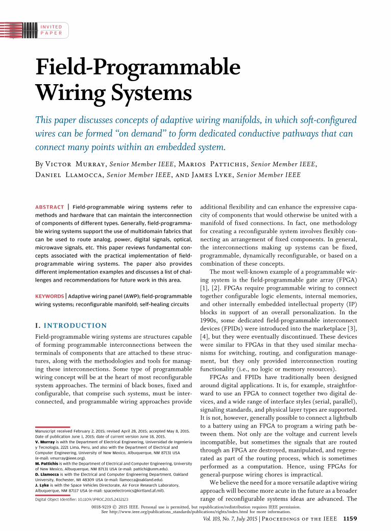
days of FPGA architectures [32]. Some elementary fabric
concepts are shown in Fig. 10. A variety of heuristic strat-
egies have been applied to counter the quadratic growth,
such as fat tree, mesh of trees (MoT), and tree of meshes
(ToM) implementations [33]. Most of the approaches re-place a bruteforce crosspoint [Fig. 10(a)] with a segmented
hierarchy of switch boxes [Fig. 10(b)]. The design of
switchboxes also benefit from some principled design
strategy. Neither a fully populated [Fig. 10(c)] nor a
sparsely populated [Fig. 10(d)] are adequate [34], but
rather some intermediate density of switches [Fig. 10(e)]
chosen by some heuristic method [35], [36] are typically
Murray et al.: Field-Programmable Wiring Systems
1168 Proceedings of the IEEE | Vol. 103, No. 7, July 2015
used in switchbox design [37]. While these design strate-
gies provide a methodology for reducing the explosion of
wiring resources, they do not address the question of heu-
ristics in fabric design regarding what is ‘‘good enough’’ forpractical purposes. It is largely a question of resource ba-
lance between wiring supply and wiring demand. The
notion is straightforward: if the fabric supplies either too
many or too few resources for most user designs, then
there is an imbalance. In other words, fabric design is
about supply and demand. If fabrics address the supply side
of the equation, then benchmarks, as a collection of typical
user designs, address the demand side.The answer is not totally satisfying since benchmarks
are empirical and must be curated. Over time, particularly
when the complexity scale of typical systems grow, the
benchmarks (if not refreshed) becomes stale, which was
the experience of the FPGA industry [38]. It would be more
satisfying if more formulaic guidelines existed, and some
have indicated that empirical relationships, such as Rent’s
rule, can better inform the design of wiring architectures.Rent’s rule is a power law relationship between the number
of modules and exterior terminals in a system
T ¼ k �Mp (1)
where T is the number of terminals, M is the number of
modules, k is a constant, and 0 G p G 1 is so-called Rent’s
exponent. The effect of Rent’s rule [39] on architecture has
been extensively discussed [40] for FPGA design.
The picture is further complicated in the more gener-
alized wiring systems that include multidomain and
multipanel fabrics. Generalized wiring architectures aremultidomain fabrics, representing a mixture digital, power,
analog, and microwave signals. As we have discussed, field-
programmable wiring systems can be in a distributed form.
These concepts represent enhancements over the basic
FPGA routing concepts discussed so far. They are also
amenable to graph-theoretic treatments. However, tradi-
tional FPGA routing algorithms would require extension to
accommodate these additional features.
F. Multidomain WiringFor each signal type, we also have a corresponding
switch type. Thus, the implementation of multidomain
fabrics requires the consideration of the distribution of
different switch types. Typically, the fabric would include a
small number of expensive power switches and a much
larger number of digital switches. Beyond switch types,routing introduces additional issues that need to be dealt
with. For example, analog and microwave routing requires
that we deal with resistance build up, line length adjust-
ment, and impedance tuning. Many of these could be
represented using switchable circuits, such as binary resis-
tive ladders to form a tunable resistance or selectable true-
time delays.
G. Multipanel WiringIn multipanel programmable wiring systems, each
panel independently contains programmable wiring re-
sources. In many respects, the challenges in developing
multipanel programmable wiring systems are similar to
those in multi-FPGA systems. In multi-FPGA systems
(driven by large-scale hardware emulation applications
[41], [42]), problems in partitioning large designs [43],performing pin assignment [44], and ‘‘spread-net’’ (nets
cutting across two or more FPGAs) routing [45] have been
studied. Just as there are non-unique solutions to the rout-
ing problem within a particular programmable wiring sys-
tem, there are also non-unique solutions to the global
partitioning of the wiring problem into subproblems. This
sort of global/local problem at a large scale is analogous to
that of the global/detailed routing problem for monolithicFPGA devices [46].
IV. SUMMARY OFEXPERIMENTAL DEVELOPMENTSIN FIELD-PROGRAMMABLE WIRING
In this section, we describe three generations of adaptive
wiring research spanning two decades, sponsored by theAir Force Research Laboratory (AFRL) and one of its
precursor organizations (Phillips Laboratory). The original
impetus for early Phillips Laboratory investments in adap-
tive wiring research (mid-1990s) was the pursuit of fault-
tolerant spacecraft design. The period was marked by large
investments in MEMS technology development [domi-
nated by the Defense Advanced Research Projects Agency
Fig. 10. Elementary fabric concepts. (a) Brute force routing.
(b) Segmented hierarchical fabric. (c) Fully populated switchbox.
(d) Linear population. (e) Heuristically determined population.
Murray et al. : Field-Programmable Wiring Systems
Vol. 103, No. 7, July 2015 | Proceedings of the IEEE 1169
(DARPA)], and the laboratory studied promising MEMS-based latching switch designs employing thermal actuation
and high aspect ratio (e.g., low resistance, high current
handling) planar, metal-to-metal contact geometries.
Since the switch designs supported nonvolatile reconfigu-
ration and could be formed at relatively high densities
(> 1000 switches/cm2), the idea of creating smart wiring
systems seemed a natural application. During that time,
members of the AFRL research team already had ex-perience with one of the Aptix prototyping systems [25], in
which printed wiring boards employed several FPID
devices and prototyping regions. Using this arrangement,
components mounted to the prototyping regions could be
interconnected by programming the FPIDs through a
configuration interface.
The original concept for an exploratory adaptive wiring
manifold based on MEMS would involve adapting theAptix board concept, replacing the volatile FPID devices
with more robust, nonvolatile versions based on MEMS
switches. It was believed that such a system would be
useful as fieldable wiring system, since the wiring patterns
could remain formed once configured (with bistable non-
volatile switches), and the switches would be capable of
sustaining wider voltage and frequency ranges than the
complementary metal–oxide–semiconductor (CMOS)-based switches present in the Aptix FPIDs. Such a concept
could be adapted to replace traditional boards and wiring
harnesses, just as FPGAs had begun to find their way into
an increasing number of production systems. These early
sentiments provide impetus for a body of work spanning
nearly two decades, described in this section.
A. Initial Conceptual DefinitionIt was envisioned that the original adaptive wiring sys-
tem would be based on several implementation principles.
1) Creation of a relatively dense MEMS switch array
with the configuration management system in the
same package. A density goal of 100 latching
MEMS switches/cm2 was deemed a ‘‘modest’’ goal.
2) Development of a flexible wiring system archi-
tecture, based on prebuilt printed circuit boards(and eventually wiring harnesses) that would ex-
ploit an intelligently arranged distribution of
terminals in blank (unpopulated) regions for
mounting components, modules, boxes, etc. These
boards would support the aforementioned multi-
chip modules (MCMs) with the necessary daisy-
chain connections and host interface to support
external configuration.3) The development of offline and eventually em-
beddable routing synthesis tools set to compute
and transmit desired wiring configurations to the
adaptive wiring manifold system. The tools, con-
sistent with those for previous FPID devices,
would accept as inputs the adaptive manifold de-
tailed configuration and the user netlist specifica-
tion, generating as output a bitstream sequence ofswitch closures.
For practical use, such adaptive wiring systems would
ideally support other useful features.
1) Dynamic reprogrammability, to support in-system
changes, especially for self-healing/fault recovery,
as well as temporary diagnostic probes (which
could be implemented either in development or
even remotely in a fielded system). This featurewould require the MEMS switches be reversible
and reprogrammable many times. As the original
notions were that this in situ reconfiguration would
be done episodically (as opposed to continuously),
it was felt arbitrarily that the ability to support
several thousand switch cycles would be sufficient
over a typical product life. This led to the definition
of switches supporting ‘‘configuration grade’’ use(103 cycles) as opposed to continuous operation
(ideally infinite cycles). The desire for in situ ope-
ration would bring other challenges, since arcing
phenomenon effects could sharply limit the life-
time of typical relay switches, especially for devices
with microscopic contact geometries.
2) The ability to diagnose the state of current config-
urations in a nonvolatile array. Since it was envi-sioned that smart wiring assemblies could be used
in production systems and that the wiring patterns
were set semipermanently, it would be undesir-
able to refresh the configuration of thousands of
MEMS switches (which manage the connections
of power distribution networks as well as other
types of signals) upon reset. As such, a way of
being able to non-intrusively read or capture stateinformation would be useful.
Since often MEMS and ASICs are created with distinct
semiconductor processes, the MEMS-based FPIDs would
be implemented as multichip modules in a ball grid array
(BGA) package, using an arrangement shown in Fig. 11,
involving one or more MEMS switch crosspoint arrays
(with an empirically chosen switch populations strategy)
and a controlling sidecar ASIC to provide a host JTAG [47]control interface and to generate the detailed time se-
quenced voltage patterns necessary to isolate its set of in-
dividual switches. As several such FPID MCMS would be
involved, the sidecar ASIC would be designed to support
daisychain connections to permit configuration as a single
extended bitstream. To capture student information (as
well as any programming firmware for the sidecar ASIC), a
small nonvolatile memory would be included in the MCMfloor plan.
B. First GenerationA first generation in adaptive wiring research (�1994–
2002) explored how MEMS switches could be integrated
into wiring structures that themselves were integrated into
the structural panels, in effect the first attempt (known
Murray et al.: Field-Programmable Wiring Systems
1170 Proceedings of the IEEE | Vol. 103, No. 7, July 2015

to the authors) to create a field-programmable wiringharness.
1) Switch Research: The switches in development for the
first-generation panel project targeted the following
properties:
• nonvolatile, having persistent (open and closed)
bistable properties;
• low contact resistance;• wide bandwidth, including dc operation;
• high current handling capacity (several hundred
milliamperes);
• ability to support live switching;
• cycle life > 10 000 operations.
During this period (mid-1990s), there were three domi-
nant classes of MEMS approaches for actuation: electro-
static [23], piezoelectric [48], and thermal [24].Electrostatic approaches usually involve high-voltage (but
low-amperage) actuation, which complicate implementa-
tion in traditional CMOS circuitry. Electrostatic actuators,
furthermore, are not optimized for high contact force,
usually resulting in poor metal-to-metal contacts and
therefore dc performance. Countering low contact resis-
tance usually involves using high force, long throw actua-
tion mechanisms. Piezoelectric actuation mechanisms,while having potential, were not explored. Thermally ac-
tuated MEMs switch configurations were deemed a good fit
for this work, since they supported CMOS-level actuation
voltages, high contact forces, and bistability. One promis-
ing configuration is shown in Fig. 12 that appears to address
most of these requirements. This switch achieved bist-
ability through two long-throw lateral thermal actuators,
one to set the switch into each stable state, as shown inopen [Fig. 13(a)] and closed [Fig. 13(b)] configurations.
Unfortunately, the thermal MEMS relays explored in the
early work, while promising, suffered from undercutting
effects during manufacture that rendered the actuation
mechanisms ineffective. While the contacts themselves
Fig. 12. Bistable MEMS switch design with two lateral thermal
switches. (a) Open. (b) Closed.
Fig. 11. Multichip module implementation of MEMS-based FPID. This module contains one or more MEMS switch crosspoint arrays and a
controller sidecar ASIC.
Fig. 13. The ‘‘liquid manifold’’ packaging concepts. (a) Component
level land grid array (LGA). (b) Panel LGA pattern. (c) Panel structure
design with mounting zones for modules.
Murray et al. : Field-Programmable Wiring Systems
Vol. 103, No. 7, July 2015 | Proceedings of the IEEE 1171

were viable (verified through manual actuation), the switchdesign was abandoned.
2) Architecture Research: Even in the earliest work, phy-
sical panel concepts were chosen to conform to a notion of
multifunction structures [49], in which the structures
necessary to build platforms (such as a spacecraft) would
also support other functional roles. These panels could be
thought of as a load-bearing circuit board panels, and it wasaim in early research to make these smart wiring panels
reconfigurable. A typical configuration research in this pe-
riod involved some features shown in Fig. 13, including
land grid array (LGA) mounting surfaces for modules
[Fig. 13(a)] as well as the panel [pattern shown if
Fig. 13(b)]. As suggested in our earlier discussion, mount-
ing areas would be designated on the panel [Fig. 13(c)] for
the attachment of modules. Some of the early architectureresearch to accompany the physical structures was referred
to as ‘‘liquid manifold’’ [50], in which dynamic permutation
routing switch boxes were demonstrated using Xilinx
FPGAs, in effect embedding one programmable structure
within another, the former being controlled by simple
commands.
3) Demonstration Implementations: Due to the inability toobtain suitable MEMs switches, conventional macroscopic
discrete latching relays were used to implement a simple
multitiered wiring system design (supporting episodic re-
configuration as opposed to dynamic), prototyped on
printed circuit boards. The control circuitry included fea-
tures to keep track of switch state, so that it would be
possible to query wiring system configuration details. This
implementation, described in [47], while not remarkablein breaking practical ground, provided useful insights for
subsequent work.
C. Second GenerationIn a second generation (�2002–2010) of adaptive wir-
ing research, AFRL-sponsored research explored more ad-
vanced MEMS switches and an improved understanding of
key architectural issues, such as wiring demand. Panel re-search evolved in parallel to form a construction method-
ology used in a line of conceptual research spacecraft.
1) Switch Research: Renewed attempts were made to
create suitable MEMS devices. A primary concern were
creating nonvolatile bistability mechanisms with high-
quality contact surfaces, leading to dedicated research
activities to study long throw actuators [51] and nanoscalecontact surface structure [52]. To address contact degrada-
tion during live switching, purchased to mitigate arc for-
mation were examined, such as using sacrificial contacts,
either with an ‘‘arc gettering’’ whisker or entire dedicated
redundant switches (to draw the arc, thus preserving con-
tact surface degradation in the primary switch). A MEMS
switch design, based on electromagnetic actuation, was
developed [53] (through a concept proposed by Magfu-sion) as a promising candidate. While the switches did not
provide new answers to live switching reliability, they did
exhibit adequate current handling and bistability [54].
2) Architecture and Panel Research: The panel architec-
ture research conducted during this time involved a set of
eclectic studies, including investigations of wiring demand
and routing architecture studies.Approximately 600 nets comprising the TacSat2 space-
craft wiring harness database were measured and histo-
grammed, revealing a power law relationship analogous to
Rent’s rule relationship previous described for microlec-
tronics. Even to the present, the authors are not aware of
other analysis work done on wiring demand in spacecraft
or other vehicular platforms, and it may therefore be pre-
mature to conclude that the scale-free model universallyapplies to is broader class of wiring system designs.
Work sponsored at Cambridgethrough a U.S. Air Force
(USAF) research grant led to the discovery of a simple but
elegant methodology for self-healing wiring systems that
employ dynamically reconfigurable routing [55]. The con-
cept involves performing a periodic sweep through a wir-
ing system in which each switch is tested for continuity
(connections involving live wires are bridged redundantlybefore separating them in the test). When bad switches are
found, they are removed from the associated wiring re-
source graph.
Additional work began to explore embedding wiring
systems into the structural panels of a spacecraft in support
of research in plug-and-play spacecraft. This work was
based on extending earlier research to develop pegboard-
like panels for spacecraft. Wiring assemblies to accommo-date the distribution of electrical power and data connec-
tions (to nonblocking Spacewire [56] packet routers) were
embedded into each of several panels forming the boxlike
structure of a spacecraft. It was envisioned that such panels
can be inventoried for the on-demand construction of
spacecraft. Components would be pulled from inventory
and mounted to panels using the standard grid convention,
aligning to and blind mating with connectors in an attemptto realize a cableless (or hidden cable) spacecraft.
3) Demonstration Implementations: A second-generation
wiring panel system, referred to as adaptive wiring mani-
fold 2 (AWM2), was created using �250 Magfusion bista-
ble electromagnetic relays distributed over two large circuit
boards. Connected together, these two AWM2 panels were
demonstrated to form nonvolatile wiring connections forpower and high-speed digital signals.
A parallel set of adaptive wiring designs were explored
for the space plug-and-play architecture (SPA) [57] re-
search program in which spacecraft were rendered as a set
of structural ‘‘smart’’ panels (onto which modular compo-
nents were mounted). A sequence of three demonstration
systems were developed. The first of these, referred to as
Murray et al.: Field-Programmable Wiring Systems
1172 Proceedings of the IEEE | Vol. 103, No. 7, July 2015

the concept bus, implemented a six-panel box demonstra-
tion (Fig. 14), using mock spacecraft modules (with elec-
trically active interfaces to study plug-and-play networkconcepts). Routing and configuration management elec-
tronics were contained in separate boxes that were at-
tached within the interior. The second demonstration
system, referred to as plug-and-play satellite (PnPSat) [58]
recessed routing circuitry inside the panels for power,
data, and testing circuitry. A third demonstration (PnPSat
2) [59] did not introduce new concepts, but involved a
hexagonal eight-panel (versus the six-panel PnPSat) con-figuration with electronics ruggedized for use in space en-
vironments. In each of the SPA panel designs, modules
were surface mounted on a 5-cm x–y pegboard grid con-
vention. As shown in Fig. 14, both blind-mated (modules
cover and complete a socket connection when mechani-
cally attached) and jumpered (module placed near a socket
and connection is completed with a short cable) connec-
tion styles were supported. This particular blind matingstrategy was ineffective, as it limited geometric flexibility
in module placement and the self-aligning notion of the
mechanical grid did not work well in practice.
Each panel design provided eight component docking
ports, supporting power [60], data, and test connections.
Each of the adaptive panel structures in the SPA research
project comprised a limited, multidomain adaptive wiring
design. As shown in Fig. 15, each panel featured a numberof ports, most intended for connection by surface-mounted
modules, with two sites reserved for interpanel connec-
tions. Each port contained connections to three limited
domains, the first being power (only 28VDC), the second
being a Spacewire [56] packet routing link, and the third
being a serial testing interface, which allowed system-wide
injection/query operations in a manner analogous to a JTAG
[47] interface. In principle, systems could be composed of
many panels, but geometries for simple spacecraft dictated alimited number (e.g., six or eight, typically).
D. Third GenerationTwo trends marked the third generation of adaptive
panel research (�2010–2014): 1) increased flexibility and
pin mapping; and 2) movement to distributed, fine-grained
(cellular) adaptive panel tiles. Some switch research was
carried out, though no viable high-density MEMS switches
were employed in any of the demonstrations.
1) Switch Research: Soon after the AWM2 demonstra-
tion, the switch vendor left the market. Several attempts
were made to find alternate vendors, and some of these
companies also stopped producing MEMS switches. Some
work continued on alternate electrostatic switches, despite
their aforementioned limitations. AFRL was also involved
with DARPA on some promising new switch designs,based on liquid metal (e.g., gallium [61]) contacts. Such
switches appear to solve the contact reliability problem
[62], since the contact surface is continuously reformed.
However none of these alternatives were available in suf-
ficient quantities, and instead, we employed the use of tiny
(�2 mm � 2 mm) solid state relays in the adaptive panel
demonstrations.
2) Architecture and Panel Researcha) Flexible pin mapping: The ability to flexibly blind
mate black box modules to panels (after the strategy sug-
gested in Fig. 5), while not an essential requirement in
field-programmable wiring systems, complements many of
the same intrinsic goals: flexibility, rapid systems forma-
tion. It also reduces exterior cabling, though not necessa-
rily a decrease in overall systems complexity (owing to theincreased overhead necessary to programmably map pins
between modules and panels). Despite the increase in
Fig. 14. A spacecraft ‘‘concept bus,’’ used to study modularization
of plug-and-play spacecraft with integrated wiring, illustrating
pegboard panel conventions, and a number of mounted components.
Equipment rack in background operated test bypass circuitry.
Fig. 15. Simple, multidomain panel design used in space plug-and-play
architecture (SPA) research. In this example, each panel contains a
number of ports. Each port contained connections to three limited
domains: 1) power (only 28VDC), 2) a Spacewire [56] packet routing
link, and 3) a serial testing interface, which allowed system-wide
injection/query operations in a manner analogous to a JTAG [47]
interface.
Murray et al. : Field-Programmable Wiring Systems
Vol. 103, No. 7, July 2015 | Proceedings of the IEEE 1173

complexity, it could also improve reliability, since havingprogrammable pin mappings allow for the inclusion of
redundancy in both panels and modules, therefore provid-
ing non-unique opportunities for such mappings. In con-
trast, traditional pin and socket assemblies do not typically
have the ability to cover from a failed connector. Adaptive
pin mapping in field-programmable systems encompasses
mechanical attachment (locations were modules may be
physically mounted), electrical discovery, and pin map-ping. The blind mating approach shown in Fig. 14 is the
most brittle form, requiring mounting in a specific location
and orientation (but providing robust attachment through
traditional fasteners and electrical connectors). Overcom-
ing these limitations requires the introduction of new
concepts, and many are based on grid conventions, in
which the periodic lattice of surface points provide op-
portunities for electrical and/or mechanical connection.Approaches such as ‘‘autoconnect’’ [63] suggested a Velco-
like press-fit connection, for example. Other possibilities
include the use of pin grid arrays (PGAs) or LGAs, the
latter combined with interposers along with mechanical
fasteners to provide force necessary to maintain good
electrical contact. When serviceability is not a concern
(i.e., modules once placed are permanently mounted),
other options (such as ball grid array and underfilling) maybe attractive.
In a study targeted for PnPSat [64], a design was de-
veloped to replace panels (such as Fig. 14) containing a
distribution 24 mounting sites were allocated as a distri-
buted contact array system. Each site employed a contact
distribution as shown in Fig. 16, with a symmetry to accom-
modate any 90� rotation. While the work was promising,
only limited work was completed toward this demonstrationpanel design in the second-generation activities.
b) Cellular tile implementation of adaptive wiringpanels: For the core developments of the third-generation
adaptive wiring panel research, we turned our attention to
more generalized (beyond PnPSat) implementations of the
cellular wiring strategies suggested in Fig. 17. We arrived
at the following set of concepts [18], [65], [66]: 1) cell
units (the basic tile building blocks); 2) cell management
units (CMUs); 3) modules represented components that
plug onto tiled arrays; and 4) some notion of a global
system to orchestrate tile collections and mapping netlists
to the tiles. These generalized schemes focused on solving
free-form programmable wiring problems, in multiple do-
mains (digital, power, analog, microwave), not the more
limited ones exemplified in the PnPSat research. While amore detailed exposition of these concepts as they apply to
specific embodiment is given in [18], [65], and [66], we
provide an abstracted representation of the concepts here.
The general cell architecture consists of the external
physical interface and the functional interface. One ap-
proach to the physical interface is shown generically in
Fig. 18, in terms of the tileable surface presented for con-
nection by surface-mounted components. Here, we showthe surface as being the intercalation of three grids: 1) a
mechanical mounting grid (the coarsest grid); 2) a power
terminal grid; and 3) a signal grid. The ratio and spacing of
contacts in each grid can be set according to wiring supply
and demand considerations. The functional unit in a gene-
ric sense is shown in Fig. 19. Each unit cell contains: 1) the
CMU; 2) a pool of wiring resources, including switch ma-
trices that may be differentiated by functional domains orother considerations; and 3) a set of terminals, with dis-
tinct terminals for surface-mounted connection and other
terminals for intercell routing.
The CMU, which controls the switch configurations
responsible for setting wiring pathways, manages three
distinct types of communications. The first of these is a
global interface, which manages commands for setting
partial netlist assignments (i.e., a portion of a masteroverall netlist mapped over all titles), conveying the status
of detected surface-mounted modules, and other aspects of
health and status relating to unit cells. The second type of
communication is intercell, managed in our work through
dedicated links to each nearest-neighbor cell. The finalFig. 16. Pin conventions for distributed contact arrays for prospective
use in PnPSat [64].
Fig. 17. Adaptive wiring panel (AWP) concept [18], [65], [66]: 1) cell
units (the basic tile building blocks); 2) cell management units (CMUs);
3) modules represented components that plug onto tiled arrays; and
4) some notion of a global system to manage the set of tiles and to
netlist the modules.
Murray et al.: Field-Programmable Wiring Systems
1174 Proceedings of the IEEE | Vol. 103, No. 7, July 2015

type of communications is a special accessory function,simply called a discovery interface. This interface estab-
lishes a systematic approach for detecting mounted mod-
ules and extracting their details.
We use the generic term module to denote surface-
mounted components that conform to the conventions
described here. A typical module will be designed to ad-
here to the mechanical, power, and signal distribution
conventions of the generic panel system. It could be assimple as a single discrete component, such as a resistor, a
battery, or a light bulb. It could also be a complex camera, a
processor, or other electronic system. The modules may be
small (fitting within a single tile) or may span multiple
tiles. A number of mechanisms could be used to detect the
presence, but we have adopted a discovery interface as
being the most versatile method. This interface can be
used to identify an arbitrary variety of details regardingsurface-mounted components, but minimally would in-
clude physical aspect information (describing the surface
shape reserved by the placed component) and identifica-
tion and grid location of terminals. Other useful informa-tion could be embedded, including URLs to maintenance
repositories, data sheets, etc.
The role of the global unit is to coordinate a notion of
over-arching netlist, manage placement and routing ope-
rations, as well as capture knowledge of the tile distri-
butions and characteristics and adjust the configuration
details as they pertain to tiles. There are many considera-
tions in the development of the global management infra-structure, including: 1) the allocation of routing details to
individual tiles; 2) support for dynamic discovery of placed
modules and route reconfiguration (as opposed to static
placement and routing); 3) ability to accommodate dy-
namic topology changes in tiles; and 4) ability to accom-
modate redundant modules (potentially ignored and
unconnected until potential need). Our inclusion of a dis-
covery interface presupposes a type of dynamic interac-tion, though this is not strictly necessary in the cases where
static compilation is involved. We have also presumed the
notion of an external tool managing the overall configu-
ration of the tile set. A far more intriguing (but presently
unexplored) possibility is a distributed implementation of
these functions, in which a single tile or group of tiles
negotiates these functions without need of an external
master.
3) Demonstration Implementation: We implemented a
48-tile version of a cellular adaptive wiring system (re-
ferred to as AWM3) embodying many of the principles
described in [18], [65], and [66], shown in Fig. 20. The
surface of this AWP, implemented as a large printed circuit
board, was created in a 6 � 8 configuration, shown in
Fig. 20(a), with four placed modules. Connectivity andphysical attachment were accomplished through PGAs
(pins on modules, sockets on the panel contacts). The
modules [Fig. 20(b)] were also implemented as smaller
circuit boards, which could be flexibly arranged in arbitrary
positions and rotations on the larger surface panel. An
external computer implemented the global controller
(managing the netlist translating and implementation of
switch closures in tiles necessary to implement the desiredwiring patterns), and i2c interfaces were used for all of the
communication interfaces. Approximately 5000 discrete
solid-state relays were used, leading to very large unit cells
whose bulk was projected below the mounting surface for
modules [Fig. 20(c)].
V. SUMMARY OF FIELD-PROGRAMMABLE WIRING SYSTEMS
A summary of the panel developments described in this
paper is shown in Table 3, spanning approximately a two-
decade period. Essentially two types of adaptive panels
were developed. The first of these, the AWM series, were
intended to support free form wiring of arbitrary signal and
power conductors. Their sophistication grew from a single
Fig. 18. Generic tile array conventions for mechanical, power, and
signal grids.
Fig. 19. Functional representation of unit cell. The unit cell transfer
information with the CMU. The unit cell contains three grids: 1) a
mechanical mounting grid (the coarsest grid); 2) a power terminal grid;
and 3) a signal grid.
Murray et al. : Field-Programmable Wiring Systems
Vol. 103, No. 7, July 2015 | Proceedings of the IEEE 1175

panel to a cellular implementation involving 48 panels. The
second type of adaptive panel, the PnPSat series, was de-
signed to manage a very limited range of signals (the dis-tribution of fixed voltage, along with specialized LVDS and
RS-422 signaling). In all of these designs, panels were in-
tended to hide interior complexity, presenting a planar
mounting surface to support mechanical and electrical at-
tachment of modules. In early versions (up to AWM2), no
discovery features were supported for modules. Although
the panels supported dynamic reconfiguration, all switch-
ing actions were manually interpreted, so that any changesin component placement would not be automatically de-
tected. Later adaptive panel work supported the automatic
discovery placed modules, such that it is possible to relocate
modules, place redundant copies, and support scaling to
much larger systems.
The variety of switch types encountered in the AFRL-
led research is summarized in Table 4. While the original
motivation for the physical implementation of adaptivewiring was based on the promise of MEMS technology,
only one adaptive wiring panel (AWM2) ever employed
them. Even in this case, the use of the switch was prob-
lematic (e.g., sensitive alignment often failing after multi-
ple solder reflow cycles). The original density goal was
> 100/cm2, but the switches used were 20� larger and
packaged form. Attempts to improve upon these limita-
tions were unsuccessful, and the company left the market-place. The pursuit of MEMS switches remained bifurcated
from the architecture research. The subsequent develop-
ments have unfortunately shown little improvement, even
nearly 20 years later. While MEMS technology has been in
a broader sense very successful, little progress has effec-
tively been made in creating practical MEMS switches with
adequate density, bistability, and reliability. In AWM3, as a
result, thousands of compact (2 mm � 2 mm) solid-staterelays were employed. While this led to a successful de-
monstration system, the overhead in the most optimistic
sense (in terms of bulk and power consumption) is unsuit-
able for practical use.
VI. RECOMMENDATIONS FORFUTURE WORK
There are significant challenges associated with the devel-
opment of the technologies that will enable the next gene-
ration of field-programmable wiring systems. We provide a
brief discussion of recommendations for future work in
this area.
Fig. 20. Images of the final AWP prototype [65]. (a) AWP with some modules placed on top. (b) A single module. (c) Side view showing the circuitry,
the panel, and the modules on top.
Table 3 Comparison of Programmable Wiring Systems
Murray et al.: Field-Programmable Wiring Systems
1176 Proceedings of the IEEE | Vol. 103, No. 7, July 2015

A. Switching TechnologiesWe have the following list of challenges for switching
technologies.
• Low-cost, low-energy relays: The key concept here
is to reduce the cost and energy requirements of
the relays so as to enable the development of larger
designs that require large numbers of relays. Over-
all, the goal here will be to provide scalable meth-ods for routing power and analog signals that can
match the success of routing digital signals in cur-
rent FPGA devices.
• Effective multipurpose switches: Currently, we
have the requirement to use different types of
switches that can route different signals. As a re-
sult, field-programmable wiring systems can be
limited by the spatial arrangement of the differenttypes of switches. Clearly then, the development of
multipurpose switches can greatly simplify the
field-programmable wiring systems design by elim-
inating the need to predetermine the distribution of
different switch types prior to deployment.
• Switches for time-shared interconnections: A sin-
gle switch can be designed to support multiple
interconnections. For example, to maintain a po-tential level using a power connection, we could
time-share to recharge capacitor circuits. As long as
the voltage level can be maintained within certain
tolerances, a single power input would then be able
to route power signals to several power terminals.
Following the development of effective switching tech-
nologies, we will have development of efficient packaging
configurations. For implementations of multidomain fab-rics, there is a need to investigate the distribution and
topology of switching types that can support different types
of signals. Techniques from survivable network design can
provide a framework that supports recovery from connec-
tion failures [8], [67]. Effective digital signal topologies
such as the methods described by DeHon [33] will need to
be extended to support multidomain fabrics.
B. Component Failure Detection and ReplacementAs with our description of the AWP, the goal has
shifted from simply interconnecting components to one of
maintaining the integrity of circuits. To support the propercircuit behavior, we need to have full support for replacing
faulty components. A basic plan for replacing faulty com-
ponents involves the following steps.
• Equivalent component library sensing: The current
implementation of the AWP [65] supports auto-
mated module component sensing. To support
component replacement, the goal will be to deter-
mine the location of equivalent components thatcan be used to replace each other.
• Working component failure detection: In order to
detect component failure, we clearly have to mea-
sure component characteristics (e.g., voltage and
current) during operation. Then, a significant de-
viation from normal operating values can be used
as a detector of component failure.
• Failed component replacement through rerouting:Once component failure has been detected, an
equivalent component can be used to replace it.
C. Circuit Integrity ManagementTo maintain circuit integrity in future panels, there is a
clear need to implement the following functionalities.
• Circuit connection diagnostics: The goal here is to
detect connection failure.
• Circuit shutdown: Once a faulty connection has
been detected, the safest step will be to shutdown
the circuit to prevent damage.
• Circuit reboot: Each circuit will then have to im-plement a reboot mechanism to support recovery.
• Live circuit recovery using dynamic partial recon-
figuration: This is an extension of the current AWP
system [65] that supports recovery from module
replacement. We also borrow the term ‘‘dynamic
partial reconfiguration’’ from FPGAs to emphasize
live circuit recovery without the need to shutdown
Table 4 Switch Types Examined
Murray et al. : Field-Programmable Wiring Systems
Vol. 103, No. 7, July 2015 | Proceedings of the IEEE 1177

and reboot. Thus, if possible, live circuit recoverywould be preferred from the requirement to shut-
down and reboot.
• Circuit connection rerouting: Once a failed con-
nection has been detected, the connection will
need to be rerouted (if possible).
• Circuit component replacement: Based on the
component diagnostics, we need to provide the
ability to replace faulty components using equiva-lent components.
D. Circuit Operation ManagementThe current implementation of the AWP cannot recov-
er from failure of the CMUs. In future research, it is im-
portant to consider the development of technologies that
can support recovery from CMU failures.
• Remote circuit management: Starting from the factthat the most basic connectivity problems are NP-
hard, it is clear that implementing larger circuits
become prohibitively expensive. To support future
growth, it makes sense to avoid the limitations as-
sociated with the computational resources of the
programmable wiring panels. Instead, we will need
methods to communicate the problems to larger
scale computational systems that can then commu-nicate the solutions. We use the term ‘‘remote cir-
cuit management’’ to refer to this framework.
• CMU operational failure detection: The failure of
the CMU hardware needs to be immediately de-
tected. However, it is important to note that we
also need to detect software failures. When using
remote circuit management, we can employ larger
computational resources to attempt recovery fromsoftware failures.
• Parallel and distributed circuit management: The
support of multiple CMUs will allow recovery from
single CMU failure. Here, a simple polling proto-
col can be used to detect failures. Furthermore, thepresence of multiple CMUs can support the devel-
opment of parallel and distributed algorithms. We
note that we can start from existing parallel rout-
ing algorithms based on the shortest path (e.g., see
[68]). To support recovery from failure, future re-
search can adopt ideas from the MapReduce
framework [69].
Ultimately, these concepts will need to be adopted tothe topologies that will support multidomain fabrics. Even
more interestingly, it will be interesting to investigate to-
pologies that can support effective algorithms.
VII. CONCLUSION
The paper provided an extensive review of the fundamentalconcepts and principles associated with the development of
field-programmable wiring systems. The development of
such systems has greatly benefited from seemingly inde-
pendent, yet interrelated technologies. A list of important,
enabling technologies includes: 1) the development of
switches that support different signal types; 2) network
topologies that can support complex interconnections;
3) practical routing algorithms; and 4) the recent integra-tion of many of these basic technologies using smart
module sensing and rerouting in the development of three
generations of field-programmable wiring systems. We ex-
pect that the future development of field-programmable
wiring systems will benefit from advancement in these
enabling technology areas.
In terms of hardware, the most urgent need is the de-
velopment of effective, low-cost, and low-energy consump-tion relays that can be used for routing power and analog
signals. In terms of software, we expect the recent devel-
opments in parallel and distributed algorithms to greatly
benefit the future generations of CMUs. h
REF ERENCE S
[1] S. Hauck, ‘‘The roles of FPGAsin reprogrammable systems,’’ Proc. IEEE,vol. 86, no. 4, pp. 615–638, Apr. 1998.
[2] R. J. Francis, J. Rose, and Z. G. Vranesic,Field-Programmable Gate Arrays, vol. 180.New York, NY, USA: Springer-Verlag, 1992.
[3] I-Cube, ‘‘Iqx family data sheet,’’ Jan. 1999.[Online]. Available: http://www.ic72.com/pdf_file/i/20685.pdf.
[4] R. F. Hartmann, S. J. Kopec, Jr., H.-C. So, andS.-C. Wong, ‘‘Programmable logic device witharray blocks connected via programmableinterconnect,’’ U.S. Patent 4 871 930,Oct. 3, 1989.
[5] M. J. Wale and C. Edge, ‘‘Self-alignedflip-chip assembly of protonic devices withelectrical and optical connections,’’ IEEETrans. Compon. Hybrids Manuf. Technol.,vol. 13, no. 4, pp. 780–786, Dec. 1990.
[6] J. C. McDonald, S. J. Metallo, andG. M. Whitesides, ‘‘Fabrication of a
configurable, single-use microfluidicdevice,’’ Anal. Chem., vol. 73, no. 23,pp. 5645–5650, 2001.
[7] C. Leiserson and F. Maley, ‘‘Algorithms forrouting and testing routability of planar VLSIlayouts,’’ in Proc. 17th Annu. ACM Symp. TheoryComput., Dec. 1985, pp. 69–78.
[8] C. H. Papadimitriou and K. Steiglitz,Combinatorial Optimization: Algorithmsand Complexity. Mineola, NY, USA:Courier Dover, 1998.
[9] Y. Wu, S. Tsukiyama, and M. Marek-Sadowska,‘‘Graph based analysis of 2-D FPGA routing,’’IEEE Trans. Comput.-Aided Design Integr. CircuitsSyst., vol. 15, no. 1, pp. 33–44, Jan. 1996.
[10] E. W. Dijkstra, ‘‘A note on two problemsin connexion with graphs,’’ NumerischeMathematik, vol. 1, pp. 269–271, 1959.
[11] T. H. Cormen et al., Introduction to Algorithms,vol. 2. Cambridge, MA, USA: MIT Press,2001.
[12] J. Roy and I. Markov, ‘‘Seeing the forest andthe trees: Steiner wirelength optimization
in placement,’’ IEEE Trans. Comput.-AidedDesign Integr. Circuits Syst., vol. 26, no. 4,pp. 632–644, Apr. 2007.
[13] F. K. Hwang, D. S. Richards, and P. Winter,The Steiner Tree Problem. Amsterdam,The Netherlands: Elsevier, 1992.
[14] M. R. Garey and D. S. Johnson,‘‘The rectilinear Steiner tree problem isNP-complete,’’ SIAM J. Appl. Math., vol. 32,no. 4, pp. 826–834, 1977.
[15] E. Ihler, G. Reich, and P. Widmayer,‘‘Class Steiner trees and VLSI-design,’’Discrete Appl. Math., vol. 90, no. 13,pp. 173–194, 1999.
[16] M. J. Alexander and G. Robins, ‘‘Newperformance-driven FPGA routingalgorithms,’’ IEEE Trans. Comput.-AidedDesign Integr. Circuits Syst., vol. 15, no. 12,pp. 1505–1517, Dec. 1996.
[17] S. Lei and W. K. Mak, ‘‘Simultaneousconstrained pin assignment and escaperouting for FPGA-PCB codesign,’’ in Proc.
Murray et al.: Field-Programmable Wiring Systems
1178 Proceedings of the IEEE | Vol. 103, No. 7, July 2015

IEEE Int. Conf. Field Programm. Logic Appl.,Sep. 2011, pp. 435–440.
[18] V. Murray et al., ‘‘Cell-based architecturefor adaptive wiring panels: A first prototype,’’J. Aerosp. Inf. Syst., vol. 10, no. 4,pp. 187–208, 2013.
[19] H. Hosaka, H. Kuwano, and K. Yanagiswa,‘‘Electromagnetic microrelays: Concepts andfundamental characteristics,’’ in Proc. MicroElectro Mech. Syst., 1993, pp. 12–17.
[20] D. J. Bishop, S. Jin, J. Kim, and A. G. Ramirez,‘‘Non-volatile MEMS micro-relays usingmagnetic actuators,’’ U.S. Patent 6 124 650,Sep. 26, 2000.
[21] K. Suzuki, ‘‘Micro electro mechanical systems(MEMS) micro-switches for use in dc, RF,and optical applications,’’ Jpn. J. Appl. Phys.,vol. 41, no. 6S, p. 4335, 2002.
[22] G. M. Rebeiz, RF MEMS: Theory, Design, andTechnology. New York, NY, USA: Wiley,2004.
[23] J.-E. Wong, J. H. Lang, and M. A. Schmidt,‘‘An electrostatically-actuated MEMS switchfor power applications,’’ in Proc. IEEE 13thAnnu. Int. Conf. Micro Electro Mech. Syst.,2000, pp. 633–638.
[24] M. Daneshmand, S. Fouladi, R. R. Mansour,M. Lisi, and T. Stajcer, ‘‘Thermally actuatedlatching rf MEMS switch and its characteristics,’’IEEE Trans. Microw. Theory Tech., vol. 57, no. 12,pp. 3229–3238, Dec. 2009.
[25] A. M. Mohsen, ‘‘Interconnect substrate withcircuits for field-programmability and testingof multichip modules and hybrid circuits,’’U.S. Patent 5 371 390, Dec. 6, 1994.
[26] D. Llamocca and M. Pattichis, ‘‘A dynamicallyreconfigurable pixel processor system basedon power/energy-performance-accuracyoptimization,’’ IEEE Trans. Circuits Syst.Video Technol., vol. 23, no. 3, pp. 488–502,Mar. 2013.
[27] J. Li and C.-K. Cheng, ‘‘Routability improvementusing dynamic interconnect architecture,’’IEEE Trans. Very Large Scale Integr. (VLSI) Syst.,vol. 6, no. 3, pp. 498–501, Sep. 1998.
[28] P.-H. Yuh, C.-L. Yang, and Y.-W. Chang,‘‘Bioroute: A network-flow-based routingalgorithm for the synthesis of digitalmicrofluidic biochips,’’ IEEE Trans.Comput.-Aided Design Integr. Circuits Syst.,vol. 27, no. 11, pp. 1928–1941, Nov. 2008.
[29] V. Pasham, W. Moreno, and F. Falquez,‘‘Field programmable multi chip modulesusing programmable laser interconnects,’’in Proc. IEEE Int. Workshop Rapid Syst.Prototyping, Jul. 1999, pp. 210–213.
[30] I. Kuon and J. Rose, ‘‘Measuring the gapbetween FPGAs and ASICs,’’ IEEE Trans.Comput.-Aided Design Integr. Circuits Syst.,vol. 26, no. 2, pp. 203–215, Feb. 2007.
[31] J. Cong and K. Minkovich, ‘‘Optimality studyof logic synthesis for LUT-based FPGAs,’’ IEEETrans. Comput.-Aided Design Integr. CircuitsSyst., vol. 26, no. 2, pp. 230–239, Feb. 2007.
[32] R. Wood and R. Rutenbar, ‘‘FPGA routing androutability estimation via boolean satisfiability,’’IEEE Trans. Very Large Scale Integr. (VLSI)Syst., vol. 6, no. 2, pp. 222–231, Jun. 1998.
[33] A. DeHon, ‘‘Unifying mesh-and tree-basedprogrammable interconnect,’’ IEEE Trans.Very Large Scale Integr. (VLSI) Syst., vol. 12,no. 10, pp. 1051–1065, Oct. 2004.
[34] N. Weaver, J. Hauser, and J. Wawrzynek,‘‘The SFRA: A corner-turn FPGA architec-ture,’’ in Proc. 2004 ACM/SIGDA 12th Int.Symp. Field Programm. Gate Arrays, Monterey,CA, USA, Feb. 2001, pp. 3–12.
[35] A. Aggarwal and D. Lewis, ‘‘Routingarchitectures for hierarchical field
programmable gate arrays,’’ in Proc.IEEE Int. Conf. Comput. Design, VLSI Comput.Processors, Oct. 1994, pp. 475–478.
[36] K. Fujiyoschi, Y. Kajitani, and H. Niitsu,‘‘Design of minimum and uniform bipartitesfor optimum connection blocks of FPGA,’’IEEE Trans. Comput.-Aided Design Integr.Circuits Syst., vol. 16, no. 11, pp. 1377–1383,Nov. 1997.
[37] Y.-L. Wu, D. Chang, M. Marek-Sadowska, andS. Tsukiyama, ‘‘Not necessarily more switchesmore routability [sic.],’’ in Proc. Asia SouthPacific Design Autom. Conf., Jan. 1997,pp. 579–584.
[38] E. Hung, J. B. Goeders, and S. J. Wilton,‘‘Faster FPGA debug: Efficiently couplingtrace instruments with user circuitry,’’ inReconfigurable Computing: Architectures, Tools,and Applications. New York, NY, USA:Springer-Verlag, 2014, pp. 73–84.
[39] J. Lyke and L. Owczarzak, Air Force ResearchLaboratory, personal communications.
[40] G. Parthasarathy, M. Marek-Sadowska,A. Mukherjee, and A. Singh, ‘‘Interconnectcomplexity-aware FPGA placement usingrent’s rule,’’ in Proc. Int. Workshop Syst.-LevelInterconnect Prediction, 2001, pp. 115–121.
[41] S. Takamaeda-Yamazaki and K. Kise,‘‘Flipsyrup: Cycle-accurate hardwaresimulation framework on abstract FPGAplatforms,’’ in Proc. 24th Int. Conf. FieldProgramm. Logic Appl., Sep. 2014, pp. 1–4.
[42] C. Chang et al., ‘‘Rapid design and analysisof communication systems using the beehardware emulation environment,’’ inProc. 14th IEEE Int. Workshop Rapid Syst.Prototyping, Jun. 2003, pp. 148–154.
[43] R. Arce-Nazario, M. Jimenez, andD. Rodriguez, ‘‘An assessment of high-levelpartitioning techniques for implementingdiscrete signal transforms on distributedhardware architectures,’’ in Proc. 48th MidwestSymp. Circuits Syst., Aug. 2005, vol. 2,pp. 1438–1441.
[44] S. Hauck, G. Borriello, and C. Ebeling, ‘‘Meshrouting topologies for multi-FPGA systems,’’in Proc. IEEE Int. Conf. Comput. Design, VLSIComput. Processors, Oct. 1994, pp. 170–177.
[45] A. Ejnioui and N. Ranganathan,‘‘Multiterminal net routing for partialcrossbar-based multi-FPGA systems,’’ IEEETrans. Very Large Scale Integr. (VLSI) Syst.,vol. 11, no. 1, pp. 71–78, Feb. 2003.
[46] S. Brown, J. Rose, and Z. Vranesic, ‘‘A detailedrouter for field-programmable gate arrays,’’IEEE Trans. Comput.-Aided Design Integr.Circuits Syst., vol. 11, no. 5, pp. 620–628,May 1992.
[47] J. Lyke, W. Wilson, and P. Contino,‘‘Mems-based reconfigurable manifold,’’in Proc. MAPLD Int. Conf., 2001. [Online].Available: http://www.slideserve.com/theta/presentation-to-mapld-2001-11-13-september-2001.
[48] J. Y. Park, Y. J. Yee, H. J. Nam, andJ. U. Bu, ‘‘Micromachined RF MEMS tunablecapacitors using piezoelectric actuators,’’ inIEEE MTT-S Int. Microwave Symp. Dig.,2001, vol. 3, pp. 2111–2114.
[49] E. Fosness, J. Guerrero, K. Qassim, andS. Denoyer, ‘‘Recent advances inmulti-functional structures,’’ in Proc. IEEEAerosp. Conf., 2000, vol. 4, pp. 23–28.
[50] R. Abbott, ‘‘Adaptive computer systems,’’in Proc. IEEE Aerosp. Conf., 2002, vol. 4,pp. 4-1819–4-1824.
[51] H. Jiao, ‘‘High force actuator formicro-spacecraft systems,’’ Los Gatos
Research, Mountain View, CA, USA, Tech.Rep. AFRL-VS-TR-2003-1120, Jun. 2003.
[52] J. Tringe, T. Uhlman, A. Oliver, andJ. Houston, ‘‘A single asperity study ofau/au electrical contacts,’’ J. Appl. Phys.,vol. 93, no. 8, pp. 4661–4669, Apr. 2003.
[53] J. Shen, ‘‘Novel field programmabletechnology based on latchingmicro-electromagnetic switches,’’MagFusion, Inc., Chandler, AZ, USA, Tech.Rep. AFRL-VS-TR-2003-1181, Nov. 2003.
[54] ‘‘Magfusion’s MEMS-based relay tacklesspace, cost issue,’’ EE Times, Jun. 2003.
[55] S. Thompson and A. Mycroft, ‘‘Self-healingreconfigurable manifolds,’’ in Proc. DesigningCorrect Circuits, 2006. [Online]. Available:http://www.cse.chalmers.se/~ms/DCC06/abstracts/AM.pdf.
[56] European Cooperation for SpaceStandardization (ECSS) Secretariat,‘‘Space engineering: SpacewireVLinks,nodes, routers and networks,’’ Jan. 24, 2003.[Online]. Available: http://snebulos.mit.edu/projects/reference/NASA-Generic/ECSS-E-40-12A.pdf.
[57] J. Lyke, ‘‘Plug-and-play satellites,’’ IEEESpectrum, vol. 49, no. 8, pp. 36–42, Aug. 2012.
[58] D. Fronterhouse, J. Lyke, andS. Achramowicz, ‘‘Plug-and-play satellite(PnPSat),’’ in Proc. AIAA Infotech@ Aerosp.,2007. [Online]. Available: http://arc.aiaa.org/doi/pdf/10.2514/6.2007-2914.
[59] D. Fronterhouse, K. Center, B. Strunce,T. Mann, and J. Dipalma, ‘‘PnPSat-2 SPAtechnology testbed initial results anddevelopment status,’’ in Proc. IEEE Aerosp.Conf., Mar. 2010, pp. 1–12.
[60] W. Boncyk, ‘‘Developing a distributed powerand grounding architecture for PnPSat,’’ inProc. IEEE Aerosp. Conf., Mar. 2008, pp. 1–9.
[61] M. G. Wong, ‘‘Bending piezoelectricallyactuated liquid metal switch,’’ U.S. Patent6 515 404, Feb. 4, 2003.
[62] P. Sen and C.-J. Kim, ‘‘A liquid-metalRF MEMS switch with dc-to-40 GHzperformance,’’ in Proc. IEEE 22nd Int.Conf. Micro Electro Mech. Syst., Jan. 2009,pp. 904–907.
[63] P. Joshi, B. Decker, J. Magill, and M. Hinds,‘‘Intelligent, universal, reconfigurableelectromechanical interface for modularsystems assembly,’’ U.S. Patent 7 763 995,Jul. 27, 2010.
[64] E. van Doorn and W. Nicholas, ‘‘Hybridwiring circuitry,’’ Intelligent Automation,Inc., Rockville, MD, USA, Tech. Rep.AFRL-RV-PS-TR-2009-1169, Apr. 2010.
[65] D. Llamocca et al., ‘‘Scalable open-sourcearchitecture for real-time monitoring ofadaptive wiring panels,’’ J. Aerosp. Inf. Syst.,vol. 11, no. 6, pp. 344–358, 2014.
[66] V. Murray, G. Feucht, J. Lyke, M. Pattichis,and J. Plusquellic, ‘‘Cell-based architecturefor reconfigurable wiring manifolds,’’ in Proc.AIAA Infotech@ Aerosp. Conf., 2010. [Online].Available: http://arc.aiaa.org/doi/pdf/10.2514/6.2010-3497.
[67] S. Orlowski, R. Wessaly, M. Pioro, andA. Tomaszewski, ‘‘Sndlib 1.0VSurvivablenetwork design library,’’ Networks, vol. 55,no. 3, pp. 276–286, 2010.
[68] I. Foster, Designing and Building ParallelPrograms. Reading, MA, USA:Addison-Wesley, 1995.
[69] J. Dean and S. Ghemawat, ‘‘Mapreduce:Simplified data processing on large clusters,’’Commun. ACM, vol. 51, no. 1, pp. 107–113,2008.
Murray et al. : Field-Programmable Wiring Systems
Vol. 103, No. 7, July 2015 | Proceedings of the IEEE 1179

ABOUT THE AUT HORS
Victor Murray (Senior Member, IEEE) received
the B.S. (high honors, ranked first in the class) de-
gree in electrical engineering from the Pontificia
Universidad Catolica del Peru, Lima, Peru, in 2003
and the M.S. and Ph.D. degrees in electrical engi-
neering from the University of New Mexico (UNM),
Albuquerque, NM, USA, in 2005 and 2008,
respectively.
He is currently a Professor and Chair of the
Department of Electrical Engineering at the Uni-
versidad de Ingenierıa y Tecnologıa (UTEC), Lima, Peru, and Research
Assistant Professor in the Department of Electrical and Computer Engi-
neering (ECE), UNM. He has considerable experience in developing adap-
tive reconfigurable hardware, based on field-programmable gate arrays
(FPGAs), for the Air Force Research Laboratory, and developing methods
and algorithms in medical imaging for detecting diseases in collaboration
to, mainly, VisionQuest Biomedical, Albuquerque, NM, USA and the Univ-
ersity of Cyprus, Nicosia, Cyprus. His research interests include amplitude
modulation-frequency modulation (AM-FM) methods, digital image and
video processing, medical imaging, and hardware design using very high
descriptive language (VHDL), and FPGAs.
Dr. Murray was the Research Director of the ECE’s Image and Video
Processing and Communication Lab (2009–2012). He was a recipient of
the STC.UNM Innovation Award at UNM in 2014 and 2015.
Marios Pattichis (Senior Member, IEEE) received
the B.Sc. (high honors and special honors) degree
in computer sciences and the B.A. (high honors)
degree in mathematics, both in 1991, the M.S. de-
gree in electrical engineering in 1993, and the Ph.D.
degree in computer engineering in 1998, all from
the University of Texas at Austin, Austin, TX, USA.
He is currently a Professor with the De-
partment of Electrical and Computer Engineering,
University of New Mexico (UNM), Albuquerque,
NM, USA. He was a founding Co-PI of COSMIAC at UNM. At UNM, he is
currently the director of the image and video Processing and Commu-
nications Lab (ivPCL, ivpcl.org). His current research interests include
digital image, video processing, communications, dynamically recon-
figurable computer architectures, and biomedical and space image-
processing applications.
Dr. Pattichis has been an Associate Editor for the IEEE TRANSACTIONS ON
IMAGE PROCESSING and the IEEE TRANSACTIONS ON INDUSTRIAL INFORMATICS,
and has also served as a Guest Associate Editor for the IEEE TRANSACTIONS
ON INFORMATION TECHNOLOGY IN BIOMEDICINE. He was the General Chair of the
2008 IEEE Southwest Symposium on Image Analysis and Interpretation.
He was a recipient of the 2004 Electrical and Computer Engineering
Distinguished Teaching Award at UNM. For his development of the digital
logic design labs at UNM he was recognized by the Xilinx Corporation in
2003 and by the UNM School of Engineering’s Harrison faculty excellent
award in 2006.
Daniel Llamocca (Senior Member, IEEE) received
the B.Sc. degree in electrical engineering from the
Pontifical Catholic University of Peru, Lima, Peru,
in 2002 and theM.Sc. degree in electrical engineer-
ing and the Ph.D. degree in computer engineering
from the University of New Mexico, Albuquerque,
NM, USA, in 2008 and 2012, respectively.
He is currently an Assistant Professor at
Oakland University, Rochester, MI, USA. His re-
search deals with runtime automatic adaptation of
hardware resources to time-varying constraints with the purpose of de-
livering the best hardware solution at any time. His current research
interests include: reconfigurable computer architectures for signal,
image, and video processing; high-performance architectures for com-
puter arithmetic, communication, and embedded interfaces; embedded
system design; and runtime partial reconfiguration techniques on FPGAs.
James Lyke (Senior Member, IEEE) received the
B.S. degree in electrical engineering from the Univ-
ersity of Tennessee, Knoxville, TN, USA, in 1984,
the M.S. degree in electrical engineering from
the Air Force Institute of Technology, Wright-
Patterson Air Force Base, OH, USA, in 1989, and
the Ph.D. degree in electrical engineering from
the University of New Mexico, Albuquerque, NM,
USA, in 2004.
He was in active duty military service with the
U.S. Air Force from 1984 through 1995. Since 1990, he has supported the
Air Force Research Laboratory (AFRL), Space Vehicles Directorate (AFRL/
RV), Kirtland Air Force Base, NM, USA, including its precursor organiza-
tions (Weapons Laboratory, 1990–1991, and Phillips Laboratory, 1991–
1998), in a number of capacities. He is currently technical advisor to the
AFRL Space Electronics Branch (Space Vehicles Directorate) and an AFRL
Fellow since 2008. He has lead over 100 in-house and contract research
efforts involving 2-D and 3-D advanced packaging, radiation-hardened
microelectronics, and scalable, reconfigurable computational and sys-
tems architectures, with recent emphasis on modularity and the rapid
formation of complex systems. He has authored over 100 publications
(journal and conference papers, book chapters, and technical reports),
four receiving best paper awards, and he has been awarded 11 U.S.
patents.
Dr. Lyke is an Associate Fellow of the American Institute of Aeronau-
tics and Astronautics (AIAA) and serves on the AIAA Computer Systems
Technical Committee. He was selected as recipient of the Federal Labo-
ratory Consortium award for Excellence in Technology Transfer in 1992
and for the U.S. Air Force Science and Engineering Award in Exploratory
and Advanced Technology Development in 1997 and 2000.
Murray et al.: Field-Programmable Wiring Systems
1180 Proceedings of the IEEE | Vol. 103, No. 7, July 2015