Embed Size (px)
Citation preview

Investigation of Trench Gate IGBTs in MMC based VSC for HVDC
Trench technology applied for bulk power transmission
KRUPHALAN TAMIL SELVA
KTH ROYAL INSTITUTE OF TECHNOLOGY
I N F O R M A T IO N A N D C O M M U N I C A T I O N T E C H N O L O G Y
DEGREE PROJECT IN ELECTRICAL ENERGY CONVERSION, SECOND LEVEL
STOCKHOLM, SWEDEN 2018

Investigation of Trench Gate IGBTs in MMC based VSC for HVDC
Trench technology for MMC VSC
Kruphalan Selva
2018-10-11
Master’s Thesis
Examiner Dr. Hans Peter-Nee
Academic adviser Cristina La Verde
KTH Royal Institute of Technology
School of Electrical Engineering
Department of Electrical Energy Conversion
SE-100 44 Stockholm, Sweden

Abstract | i
Abstract
The following is a thesis project involving investigation of applicability of trench type IGBTs in present and future VSC based HVDC convertors. The work involves three major sections – theoretical loss evaluation of adoption of Trench technology (both IGBT and BIGT) for HVDC Light® applications, testing the Trench IGBT prototype with existing gate units and finalizing with a hypothesis and a practical solution for unexplained turn-on phenomenon observed during testing. The thesis concludes with the suggestion of suitable driving mechanisms (e.g. reduced number of current sources and removal of active gate snubbers) which shall result in both simpler and more cost effective driving compared to the present employed methods.
Keywords
Trench-IGBT, VSC, HVDC, IGBT Driving Methods


Sammanfattning | iii
Sammanfattning
Följande avhandling är en studie om tillämpligheten av trench type IGBTer i nuvarande och framtida
VSC baserade HVDC konverterare. Arbetet omfattar tre övergripande delar – teoretisk förlustberäkning
vid tillämpning av trench teknologi (både IGBT och BIGT) till HVDC Light applikationer, prov av Trench
IGBT prototyp med befintliga gate enheter och slutligen en hypotes och praktisk lösning till oförklarliga
turn-on fenomen som observerats under prövning. Avhandlingen avslutas med en sammanfattning över
lämpliga drivningsmekansimer (t.ex om antal strömkällor och borttagning av aktiv snubber vid gate
enheten) som torde resultera både i enklare och kostnadseffektivare drivning jämfört metoder som
tillämpas idag
Nyckelord
Trench-IGBT, VSC, HVDC, IGBT drivningsmekansimer


Acknowledgments | v
Acknowledgments
I would like to extend my deep gratitude to Dr. Hans Peter-Nee and Dr. Jürgen Hafner for the
opportunity to work in this subject area. Beginning with a summer visit to the ABB HVDC, Ludvika in
2015 , they were instrumental in helping me flourish my grounds here. As a research intern in 2016 and
a thesis effort in 2017. I extend my thankfulness to Annika Lokrantz, André Bodin and Gopichand
Bopporaju to getting me started on my journey here at Ludvika.
The thesis, I gladly thank Ingemar Blidberg of Valves Development department, my supervisor and
guide on whose inputs I have steered the thesis and to mention his career expertise and experience
exceeds my age by 10 years at the time of writing this thesis should give a picture of the tremendousness
of expertise that I was given access to. The momentum I have gained during the few months in this this
field of technology has been invaluable and I thank my colleagues and a wonderful team for that. It would
be a miss not to mention Mika Sepannen for his help in testing and hour long discussions about scientific
regards, setting up the high power equipment I was enbled to use. I thank Daniel Johannesson for his
takes on interesting behavior of the Trench-technology during experimentation.
I also extend my gratitude to Munaf Rahimo, Chiara Corvace and Arnost Kopta who provided their
inputs and set direction on the start of the thesis.
Also to mention are Dr. Nathaniel Taylor, Dr. Rajeev Thottappillil, Patrik Janus for their excellent
support and inputs during the times at KTH. I also owe it to the wonderful times and discussion in the
Electrical Power Conversion Laboratory’s coffee table with Simon Nee, Nichlas and Jesper who have
always merried me with their discussions and lively company.
Ludvika, February 2018 Kruphalan Tamil Selva

6 | Table of contents
Table of contents
Abstract ......................................................................................................... i
Acknowledgments .................................................................................... v
Table of contents ...................................................................................... vi
List of Figures ............................................................................................ ix
List of Tables .............................................................................................. xi
List of acronyms and abbreviations ................................................... 1
1 Introduction ......................................................................................... 2
1.1 Motivation for DC over AC .................................................................................... 2
1.2 HVDC Light® Technology ..................................................................................... 2
1.3 HVDC Light® Topologies ...................................................................................... 3
1.4 Main Motivation ........................................................................................................ 5
1.5 Scope of the Thesis................................................................................................... 5
2 IGBT Overview .................................................................................... 7
2.1 Operational Overview ............................................................................................. 7
2.2 The Trench Gate IGBT ............................................................................................. 8
2.3 Fine tuning the IGBT for optimal losses ....................................................... 10
2.3.1 Trench vs Normal Summary ............................................................ 10
2.3.2 IGBT and thin wafer technology: .................................................... 11
3 Loss Evaluation for an MMC system ........................................... 14
3.1 Power Losses........................................................................................................... 14
3.2 Operating conditions............................................................................................ 15
3.3 Conduction Loss ..................................................................................................... 16
3.3.1 IGBT Conduction Losses .................................................................... 18
3.3.2 Diode Conduction Losses................................................................... 18
3.3.3 Other conduction losses ..................................................................... 18
3.3.4 DC voltage dependent losses............................................................ 19
3.3.5 Losses in DC capacitors ...................................................................... 19
3.4 Switching Losses .................................................................................................... 19
3.4.1 IGBT Switching losses ......................................................................... 19
3.4.2 Diode switching losses ....................................................................... 20
4 Loss Evaluation in HVDC Light® Generation 5 ...................... 22
4.1 Trend in Loss figures............................................................................................ 30
4.2 Translation in terms of cost savings: ............................................................. 31

Introduction 7
vii
5 Single Pulse Test of a Semiconductor Switch. ......................... 32
5.1 Turn on as a Circuit Perspective: .................................................................... 33
5.2 Turn Off as a Circuit Perspective ..................................................................... 35
5.3 IGBT Safe Operating Area ................................................................................... 37
5.3.1 Forward bias safe operating area (FBSOA) ................................ 38
5.3.2 Reverse bias safe operating area (RBSOA) ................................. 39
5.4 Optimization of IGBT Switching Characteristics ....................................... 39
5.4.1 Low ON state losses ............................................................................. 39
5.4.2 Low switching losses ........................................................................... 40
5.5 IGBT Turn-On switching loss ............................................................................ 40
5.6 IGBT Turn-Off switching loss ............................................................................ 40
5.7 Diode Turn-OFF switching loss ........................................................................ 41
5.8 Turn On as a Semiconductor Perspective: ................................................... 41
6 Practical Testing Single Pulse Tests .......................................... 46
6.1 Gate Drivers Employed ....................................................................................... 46
6.1.1 Voltage source driving ........................................................................ 46
Circuit for Measurement ................................................................................... 48
6.2 Commutation Inductance ................................................................................... 48
6.3 Current measurement ......................................................................................... 49
6.4 Voltage measurement .......................................................................................... 49
6.5 Measurement Summary ...................................................................................... 50
6.6 Equipment Summary ........................................................................................... 51
6.7 Heating of DUT ....................................................................................................... 51
6.8 Currents and Voltages of Test........................................................................... 52
7 Comments on the observed measurements ............................ 54
7.1 Reduction of Gate driving currents ................................................................ 54
8 Unknown Oscillations ..................................................................... 56
8.1 Discussions on the oscillations ........................................................................ 56
8.1.1 Gate side causes .................................................................................... 57
8.1.2 Device side causes ................................................................................ 57
9 Observed Test Results .................................................................... 60
10 Summary of Work Done ................................................................. 64
10.1 Further studies ....................................................................................................... 64
10.2 Conclusion ................................................................................................................ 65
References ................................................................................................. 67


List of Figures | ix
List of Figures
Figure 1: Simple scehmatic of 2 level convertor .............................................................................. 4
Figure 2: Essence of obtaining a sine from a modulated 2 level convertor ....................................... 4
Figure 3: Structure of an MMC ......................................................................................................... 5
Figure 4: Figure depicting the transistor-FET coupling on the IGBT structure [5]............................ 7
Figure 5: Cell pitch and gate depth seen in 3-dimensional perspective in a MOSFET[6]................... 8
Figure 6: Trench IGBT cross section [5] .......................................................................................... 9
Figure 7: Punch through structure of IGBT. ................................................................................... 12
Figure 8: SPT technology exhibiting lower Eoff and lower Vce ......................................................... 13
Figure 9 : Carrier Profile in SPT and SPT+ technologies [14] ......................................................... 13
Figure 10: Classification of losses in a valve. Semiconductor losses playing a significant role is color coded for emphasis. ..................................................................................... 16
Figure 11: Generalized V-I curve for the IGBT ............................................................................... 16
Figure 12: Generalized V-I curve with resistance slope depiction ................................................... 17
Figure 13: Plots depicting significant reduction in conduction losses with trench technology ....... 25
Figure 14: Plots depicting significant reduction in conduction losses with trench technology ....... 26
Figure 15: Plots depicting significant reduction in conduction losses with trench technology ....... 27
Figure 16: Plots depicting significant reduction in conduction losses with trench technology ....... 28
Figure 17: Plots depicting significant reduction in conduction losses with trench technology ....... 29
Figure 18 : Loss trend in increasing current and active power....................................................... 30
Figure 19: Figure showing extensive savings as convertor utilization increases. ........................... 31
Figure 20: Circuit of a single pulse tester. ...................................................................................... 32
Figure 21: IGBT turn-on switching characteristics ........................................................................ 34
Figure 22: Turn on event and its corresponding current path. ...................................................... 35
Figure 23: IGBT turn-off switching characteristics. ....................................................................... 36
Figure 24: Current path during DUT turn-off. ................................................................................ 37
Figure 25: IGBT safe operating area (SOA) .................................................................................... 38
Figure 26: IGBT Turn-on showing gate-voltage bump and diode reverse recovery on an inductive load [5]. ................................................................................................. 44
Figure 27: Rg driving basic circuit ................................................................................................. 47
Figure 28: Rg driving parameters influence. Source: Generic application notes of an IGBT. ........... 47
Figure 29: Preliminary runs of the turn-on. ................................................................................... 55
Figure 30: Oscillogram showing the current source switch overs during turn-off. ......................... 55
Figure 31: DUT Current and Voltage are depicted here. The turn-on exhibits a certain anomaly which is termed as turn-on notch/dip/’kink’ interchangeably. Voltage and current levels not depicted as this phenomenon varies across the ranges and is not unique to this level..................................................................... 56
Figure 32: Turn-on exhibiting a current dip in discussion. ............................................................ 60
Figure 33: Reduced current dip relative to the turn-on in Fig. 32 .................................................. 61
Figure 34: Reduced current dip relative to the the turn-on in Fig. 32 and Fig. 33 .......................... 61
Figure 35: Worsened current dip. See Fig. 32-34 ........................................................................... 62


List of Tables | xi
List of Tables
Table 2 : Table summarizing in a much generalized way of the difference between trench and planar technology. .....................................11
Table 3: Ambient condition of the valve. ......................................................... 15
Table 4: Summary of devices and Valve operating parameters ....................... 22
Table 5 : Devices undertaken for the study and their associated parameters .. 23
Table 6 : Different IGBTs and their characteristic for loss calculations ........... 24
Table 7 : Semiconductor losses in the convertor ............................................. 25
Table 8: Semiconductor losses in the convertor .............................................. 26
Table 9: Semiconductor losses in the convertor .............................................. 27
Table 10: Semiconductor losses in the convertor ........................................... 28
Table 11: Semiconductor losses in the convertor ............................................ 29
Table 12: Cost savings on employing Trench technology per station .............. 31
Table 13: List of instruments employed for measurements. ........................... 50
Table 14: List of passive components used...................................................... 51
Table 15: Temperature gradient between the DUT position and the AUX position ..................................................................................... 52
Table 16: Voltage and current combinations to conduct the test ..................... 52
Table 17: Current notch and current dependence ........................................... 58


Introduction | 1
List of acronyms and abbreviations
Aux Auxiliary Device
BIGT Bi-mode Insulated Gate Transistor
CTL Cascaded Two Level
DUT Device Under Test
Eoff_IGBT Turn-off energy of the IGBT on inductive switching with Aux device as a diode.
Eon_IGBT Turn-on energy of the IGBT on inductive switching with Aux device as a diode.
Erec_d Reverse recovery energy of the diode
Generation 5 HVDC Light® Generation 5
GU Gate Unit
HVDC High Voltage Direct Current
Ice Collector-Emitter current
IGBT Insulated Gate Bipolar Transistor
NPT Non Punch Through
PT Punch Through
RT Room temperature
SC Short Circuit
SPT Soft Punch Through
SVC Static VAR Compensator
Vcc Capacitor Bank Voltage (in pulse test circuit)
Vce Collector-emitter voltage
Vge Gate-Emitter Voltage

2 | Introduction
Chapter 1
Thesis Introduction and Scope
1 Introduction
1.1 Motivation for DC over AC
HVDC technology has been taking shape rapidly in various topologies and with the improvement of
semiconductor technology. All the developments are aimed at increasing the efficiency of power
transmission and conversion. It is interesting to note that DC lines can be operated at higher voltage
levels for the same power when compared to AC. This is because the power equivalence in an AC system
is provided by the RMS of a current for AC whereas maximum current for the DC. This means that AC
lines require more insulation clearance for the same power when compared to DC. Hence, the power
capacity can be directly increased exploiting this phenomenon. In an AC cable, an increase in the cable
length means an increase in the capacitive current. The cable hits a theoretical limit for length where
the capacitive currents can be more than the rated current of the entire line. In comparison, DC cables
have no such theoretical limit. There is also no inductive voltage drop as in AC lines. For these reasons
DC power transmission is ever increasing in its popularity. There is also a proliferation of renewable
energy sources (photovoltaics, wind farms and the likes) which need DC interconnection and power
transfer between significant distances.
1.2 HVDC Light® Technology
HVDC Light® is a HVDC transmission/reception technology with the core principle of self-commutation
involving IGBTs. It distinctly differs from its sister lineup called the HVDC Classic system where the working
principle is line commutation involving thyristors. This is because the currents can be turned on and off by the
control of the semiconductor valves unlike the Classic technology where a strong network is needed to commute
the currents [1]
HVDC Light® technology as the name implies is utilized for systems involving power transfer and control in
a short span of area and the technical requirements per se in comparison to the classic technology are much less.
The technology consists of the sending and receiving end stations with IGBT based convertors at their heart and
DC transmission lines for interconnection. This is in stark contrast to HVDC classic technology where power is
usually transmitted to very long distances and power handling involves interconnection of normal operational
grids. A short summary is provided in table 1.

Introduction 3
3
HVDC Light® HVDC Classic
Convertor Valve Technology Voltage Source Convertor
Line Commuted Convertor
Switches Employed IGBTs / BIGTs Thyristors
Power Handling 50-2500 MW 8000 MW
Employed Areas Offshore Plants to Land/ Wind Bulk power transmission
Table 1: A preliminary overview of HVDC technologies [2].
1.3 HVDC Light® Topologies
• Convertor topologies are extremely important in dictating the losses and flexibility of operation in a
HVDC system. They dictate the frequency at which the valves may be operated, the position of placement
of various core components and dictate the limitations of operation of a system [2] [3].
• A topology may allow for numerous switches with low switching frequency or high frequency with lesser
switches requirement of additional/lesser capacitors etc., voltage sharing among sub-modules. And
therefore are sole dictating factors of how a semiconductor switch maybe employed. It is therefore
important to know how the Trench Device may be a suitable candidate for the upcoming MMC.
• A very primitive run through of the type of topologies in operation is presented below to highlight the
significance of the discussion above. Each topology marks a significant mark in introduction of a
semiconductor switch / improvement with demand (topology) feeding the research in semiconductor
technology and its availability helping shaping new and better topologies every day .
Generation 1
• Generation 1 is a 2-level convertor. The voltage levels alternate between two levels in a controlled
modulation relatively with high frequency of approximately 2 kHz.
• The DC side has a ground zero to keep the harmonic content less and mitigate EMC problems.
• Such a configuration relatively highly losses due to the high frequency switching and the particular
topology. Employed switches were of 2500V/700A.

4 | Introduction
Figure 1: Simple scehmatic of 2 level convertor
Figure 2: Essence of obtaining a sine from a modulated 2 level convertor
Generation 2
• The switch ratings were improved to 2500 V/2000 A and employed in a 3-level convertor topology.
• This generation improved harmonic performance by reduced switching frequency and new
semiconductors.
• Losses are guaranteed to be less than 1.8% (station losses).
Generation 3
• Introduces a two level convertor again with optimized PWM pattern.
• Losses are guaranteed to be less than 1.4 % (station losses).
Generation 4
• This generation employs 4500V/2000 A IGBTs in the form of Cascaded Two Level Convertor.
• A general trend of higher voltage class IGBT’s being introduced is observed.
• Switching frequency were reduced hence enabling the reduction of losses up to 50 percent.
Introduction 5
5
Generation 5
Figure 3: Structure of an MMC
• Generation 5 is the topology for which the loss figures are calculated in the thesis.
1.4 Main Motivation
The main motivation of the thesis will be to investigate Trench based IGBTs as a viable device for HVDC
Light® Generation 5 system of VSC based MMC.
1.5 Scope of the Thesis
-Run preliminary loss calculations on HVDC Light® Generation 5 VSC Valve template with now present values
of trench devices.
-Document the Trench Device for their performance (Eon_IGBT, Eoff_IGBT and Erec_diode for the diode) in single pulse
testing.
- Record any anomaly (investigate for oscillations / snappiness / runaway conditions) in
behavior of the trench device with the present system of driving and propose changes and
suitable adaptations for successful and optimized switching of the device as an effort for inputs
for development.


IGBT Overview | 7
Chapter 2
IGBT Overview and the Trench Technology
2 IGBT Overview
IGBT entered the electronics market in the early 1980s. The IGBT was developed as a direct competitor to the then
existing BJTs [4]. The primary aim was to address the low current gain of the BJTs in High Voltage applications. Also in
another perspective, the usage of MOSFET structure for gate control and having the current capabilities of the BJTs proved
to be a massive success in the power industry. This points to very low on state voltages and better control of the devices.
As time progressed, attributing to many developments in manufacturing, packaging and semiconductor technology
developments IGBT are defacto choices in many area of power oriented applications presently. E.g., Drives and HVDC
applications.
2.1 Operational Overview
As mentioned above, the IGBT is a direct adoption of the power MOSFET with a minor change on the emitter side. It’s
modified to p-n-p junction template of a BJT while maintaining the MOS gate at the top of the chip. The building block of an
IGBT is a MOSFET, parasitic thyristor and a bipolar transistor. When the gate is provided with the appropriate voltage, just
like in the MOSFET, a channel ‘open up’ on the surface of the p-region below the gates. The holes from the p-region (IGBT
collector) partly combine with the electrons from the channel and this constitutes the MOS channel current that acts as the
trigger for the BJT that between J1 and J2. The remaining holes are transported via the space charge region into the IGBT
emitter (or T1’s collector)
Figure 4: Figure depicting the transistor-FET coupling on the IGBT structure [5].
8 | IGBT Overview
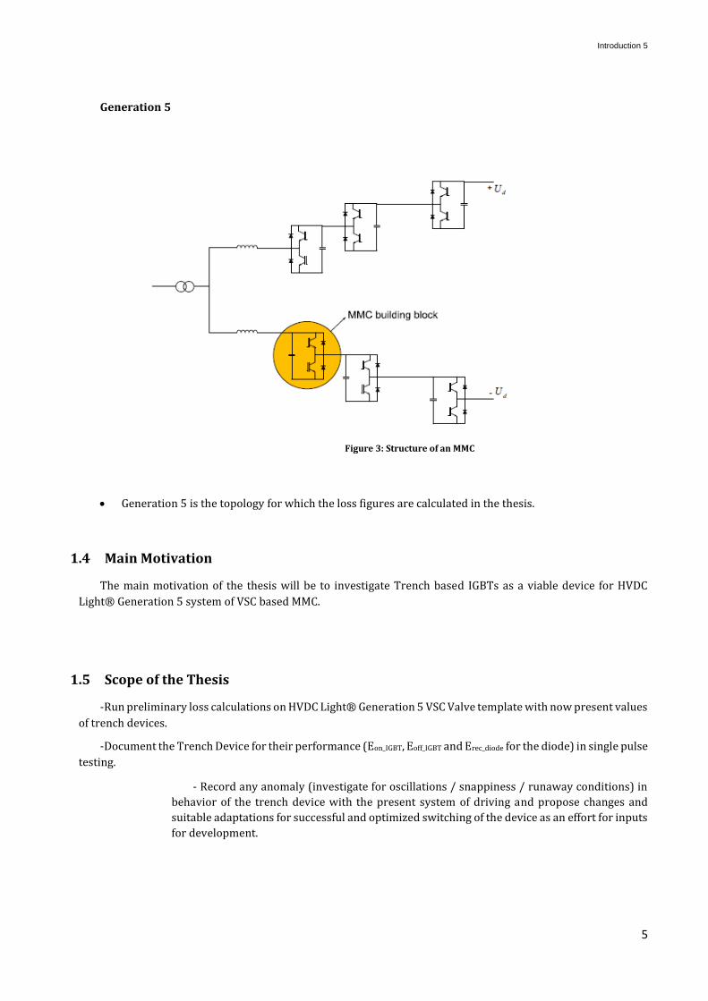
2.2 The Trench Gate IGBT
The trench type IGBT is a consequence of three requirements. An IGBT is usually limited by the parasitic-thyristor that
could latch up the device. Naturally, the devices’ footprint that could also affect the thermal capabilities and ergo the current
limitation.
1) The requirement for a Lower Vce (lower losses)
2) Reduction of the turn-off losses
3) The requirement of a higher current density capacity during operation (better device in terms
of performance capability).
Figure 5: Cell pitch and gate depth seen in 3-dimensional perspective in a MOSFET[6]
One of the natural ways to bring about the increase in the current density is the scaling of the IGBT (increase number
of IGBT per chip area). This can be done by reduction the size of a single IGBT structure to a suitable size and thereby
increasing the number of effective current capacity. However, there is a particular limit to this solution as current densities
can get larger and thermal capacities maybe a problem.
One of the many other ways that this could be established is by an intelligent solution would be to optimize the gate
structures to accommodate more IGBTs on the same chip area. If there is a possibility to etch the gates vertically into the
chip and not horizontally, while effectively maintaining considerably equal MOS channel lengths for the ‘control’ of the main
channel currents, it should result in better utilization of available chip area [5].
The trench structure was developed with this context of requirement. This proof of concept can easily be verified time
after time by simulations of simplest templates[7]. The concept of trench gates have been existent for a long time from but
their development and applicability has taken a long time attributing it to manufacturing bottlenecks and possibilities.

9
Figure 6: Trench IGBT cross section [5]
Since the structure of the gate has been modified, the device’s behavior exhibits behavioral changes too. The loss
reductions can be bought about my addressing many other aspects such as Module stray aspects[8], better internal current
distribution and current pathways both in terms of packaging[9] and semiconductor design (better conductivity
modulation)[10],and as mentioned above, the gate structures themselves. At high voltages and currents with constricted
chip area, these aspects become increasingly important[11]. Trench along with its improved losses and performance figure
have shortcomings in certain areas such as short-circuit performance [5], controllability and lifetime issues due to the
inherent structure of the gates. This thesis in the practical section (Chapter 6) is aimed at investigating these aspects and
to investigate the necessary adaptations needed to be made for easier migration of present IGBT driving systems to a trench
one.

10 | IGBT Overview
2.3 Fine tuning the IGBT for optimal losses
The above mentioned discussion talked about how changing the gate structure had brought about drastic changes in
the loss figures of the switch. Working on the base regions of the device can provide for loss optimizations too. The
parameters that need to be aimed for are the recombination times at the base region for better turn-off performances.
However, as a tight knit system, such an optimization is heavily connected to the blocking voltages of the device thereby
directly affecting the device voltage capability itself.
It is therefore interesting to discuss technologies that address these parts of the equation and can be considered
landmark development in the field of IGBTs.
ABB has been constantly improving the performances (Voltage, current ratings and losses) in its IGBT design often first
reflected in medium voltage industrial plug and play operation packaging named HiPak.
2.3.1 Trench vs Normal Summary
A summary of trench and planar gate cell relative to each other is presented here
Planar Gate Trench Gate
Gate Structure Placement Horizontal to base
Vertical to base
On-State Voltage Low Relatively low
Latch up Probability High Low

11
Channel resistance Higher Lower
Gate Capacitance Low Relatively Higher
Gate Power Consumption Low High
Controllability Good Relatively challenging due to
excessive gate capacitance
Manufacturing /
Production Feasibility
Easy Expensive
Table 1 : Table summarizing in a much generalized way of the difference between trench and planar technology.
Development on the conductivity modulation:
Conductivity modulation purely depends on the semiconductor technologies and is not the exact scope of this thesis.
However, a basic overview is discussed in these sections and a literature survey has been performed with articles
2.3.2 IGBT and thin wafer technology:
The thinner the wafer of IGBT, the better its performance in a generic sense (lower on-state drops and the likes). A
trend towards thinner wafers proves advantageous in many aspects. However, on thinning wafers requires higher field
stress withstand capacities for a given voltage. And there has been a rising trend in need for higher voltage switches.
Hence, intelligent technologies such as NPT and SPT (and FS) come into the picture. However, chronologically, Punch
through was the first to begin with.
The original PT structure:
The PT type is evident from its structural overview. It is characterized by a thick layer of p+ substrate below an n+
buffer layer (termed the punch-through layer). The presence of a n+ buffer layer renders the E-field to punch through during
a turn off event thereby cutting the tail current short in an IGBT. On an explanatory note, during the turn-off, if the field is
high enough across the collector-emitter of the IGBT, the field can trespass the n+ buffer layer and reverse bias the BE
junction of the internal pnp transistor to turn-off. Hence, they usually have lower turn-off losses. But there is a slight loss
in degree of controllability of the internal pnp transistor structure as it masks itself due to the inherent high gain achieved
on the CB junction by the n+ doping over the p+ substrate. This means that the trans-conductance of the internal MOSFET
cannot be controlled well. When added to the fact that PT IGBT exhibit lower Vce at higher temperatures, paralleling them
can be extremely challenging. PT IGBTs have lesser reverse voltage breakdown relative to their NPT counterparts. Hence,

12 | IGBT Overview
on an application point of view, PT devices are preferred where voltage reversal events are less and the device does not
need to support reverse voltages. The devices are usually of higher cost due to the epitaxial growth method employed for
die fabrication.
Figure 7: Punch through structure of IGBT.
Non Punch Through IGBT:
The NPT is distinctly different from the PT that it has no ‘buffer’ layers for the field to punch through. Also this makes
it viable to have thinner p+ substrates thereby reducing the chip’s thickness. On a fabrication point of view, this is
advantageous as simple float-zone methods can be adopted which are much cheaper compared to epitaxial growth method
employed for the PT devices.
However, as they have no PT layer, the tail currents are relatively longer exhibiting relatively higher turn-off losses.
Also, the Vce slightly higher due to lower gain on the internal transistor structure. In contrast to the PT device, as the trans-
conductance of the MOSFET is now well controllable, NPT devices are excellent candidates for short ratings. Vce increases
with temperature making it very suitable for paralleling the devices.
13
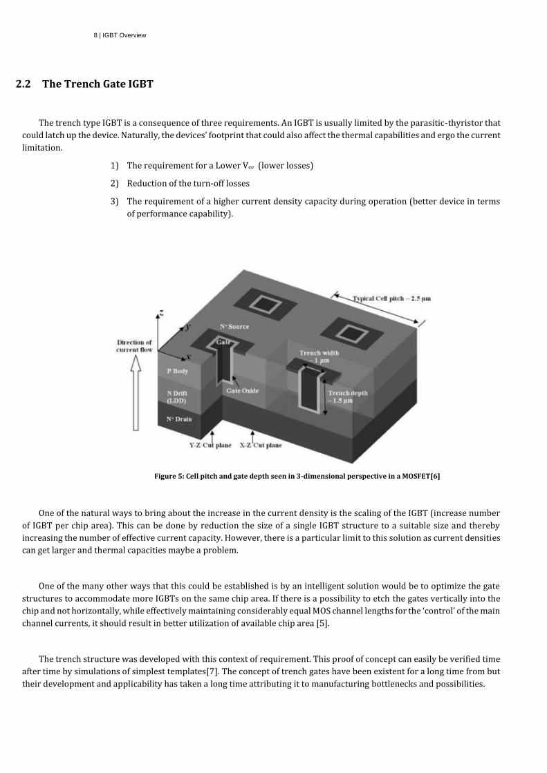
Soft Punch Through and Field Stop technologies:
The SPT (Soft Punch Through) [12] [13] and the FS (Field Stop) concepts combine the best aspects of PT and NPT for
optimal performance of the IGBT. The IGBT is managed to be fabricated as thin (or even thinner) as a NPT for lower Vce and
a lightly doped buffer layer is introduced to ‘stop’ the field as in a PT device as explained in previous section.
Figure 8: SPT technology exhibiting lower Eoff and lower Vce
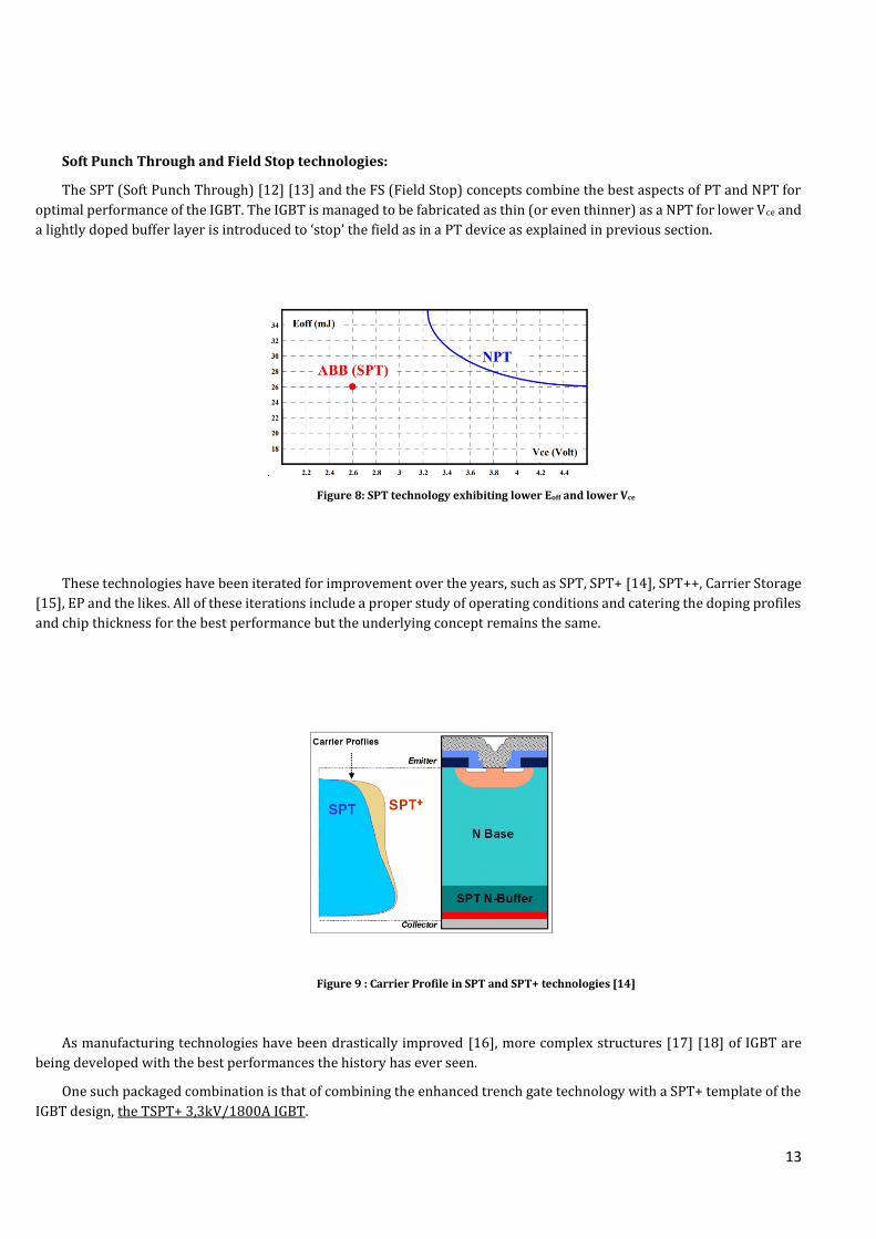
These technologies have been iterated for improvement over the years, such as SPT, SPT+ [14], SPT++, Carrier Storage
[15], EP and the likes. All of these iterations include a proper study of operating conditions and catering the doping profiles
and chip thickness for the best performance but the underlying concept remains the same.
Figure 9 : Carrier Profile in SPT and SPT+ technologies [14]
As manufacturing technologies have been drastically improved [16], more complex structures [17] [18] of IGBT are
being developed with the best performances the history has ever seen.
One such packaged combination is that of combining the enhanced trench gate technology with a SPT+ template of the
IGBT design, the TSPT+ 3,3kV/1800A IGBT.

14 | Loss Evaluation for an MMC system
Chapter 3
Loss evaluation in an MMC system
3 Loss Evaluation for an MMC system
Any convertor valve is a succeeding factor in the context of technological employment in real world
if and only if it possess a significant motivating aspect for cost efficiency. And the losses in the convertor
setup are one of the foremost aspects that determine this. It is therefore important extreme importance
in placed in the accuracy of measurement in the losses that appears during the operation.
A simple method in a very crude sense would be to evaluate the losses during the nominal operation
of the convertor by finding the difference in the transmitted and received power at any instance.
However, with HVDC systems that are presently in employment, losses are rather minimal and to obtain
such small factor in contrast to the magnitude of measured quantities will not make sense in the
fundamental principle of measurement and will not give a clear picture of the weights contributing
factors to the losses.
Hence, it becomes important to deconstruct the losses to various segments in the convertor and the
sum up the losses from a bottom-up approach. When these individual segments are considered for loss
calculations, the loss figures are more accurate because the variables involved are have direct relevance
to operational aspect of the block and not of the system.
Ambient conditions for each blocks also therefore gain immense importance in the loss calculation
involved. The following is adopted from IEC-62751.
3.1 Power Losses
A generalized loss model cannot be provided for the convertors as a thumb rule due to the presence
of numerous number of topologies and intricacies. Every individual VSC system must have its own
detailed formulation of loss calculation procedure. But in all VSC convertors, there are two main loss
contributing factors.
1) Conduction Losses
2) Switching losses
The losses can be clubbed as follows:
1) IGBT conduction losses
2) IGBT switching losses
3) Diode conduction losses
4) Diode turn-off losses
5) Snubber losses
6) Valve Electronics power consumption

15
7) Losses in DC capacitors of the Valve
8) DC voltage dependent losses
9) Other Valve conduction losses
3.2 Operating conditions
The losses depend on the operational state of convertor. The important parameters of reference are
ambient temperature, atmospheric pressure, humidity, coolant temperature, transmission conditions
(active and reactive powers) and the likes. Upon unavailability of such data, a standard reference shall
be maintained.
Parameter Condition
Dry-bulb temperature 200 C
Wet-bulb temperature 140 C
Atmospheric pressure 101,3 kPa
Table 2: Ambient condition of the valve.
The valve losses will be calculated assuming all the redundant cells are in operation. It is therefore
interesting to note that this will give the highest VSC valve loss while the losses per level is not the highest
(as it occurs when the redundant cells are bypasses/shorted).

16 | Loss Evaluation for an MMC system
Figure 10: Classification of losses in a valve. Semiconductor losses playing a significant role is color coded for emphasis.
3.3 Conduction Loss
When the IGBT or a diode conducts, there is a small amount of forward voltage drop. The product of
this voltage drop and the current through the device gives raise to ‘conduction losses’. The forward drop
is FV and
( )CE satV in IGBTs.
Figure 11: Generalized V-I curve for the IGBT
Losses
Switching losses
IGBT Diode
Conduction Losses
IGBT Diode
Losses in DC Capacitors
D.C Voltage dependent
losses
Other conduction
losses
Other losses
Snubber circuit losses

17
Mathematically,
For the IGBT,
2
_ ( )
0
1( ). ( ). ( )
2cond IGBT Igbt CE sat IgbtP I t V I d t
For the Diode
2
_
0
1( ). ( ). ( )
2cond D D F DP I t V I d t
The other approach for loss calculation would be to take into account the semiconductors’
characteristics value during their switched on state which shall be piecewise linear approximated into
two components, namely the threshold voltage Vo and slop resistance Ro. Therefore the conduction
losses can be formed as
2
0 0cond av RMSP V I R I
Figure 12: Generalized V-I curve with resistance slope depiction
where
Vo is the knee voltage
Ro is the slope resistance of the switch
Irms is operational current of the switch
Iav is the DC equivalent of the switch current

18 | Loss Evaluation for an MMC system
3.3.1 IGBT Conduction Losses
The loss in IGBT is computed as mentioned above. Unlike 2 level convertors where the number of
IGBTs are directly multiplied to per-IGBT loss to get the total loss, the loss calculation for an MMC is
complex. Since the currents are different in each cell/submodule vary, each cell has to be taken into
account for its averaged and rms currents for the loss calculation and then finally summed together.
2
0 0IGBT T Tav T TrmsP V I R I
Where
0TV is the IGBT threshold voltage
0TR is the IGBT slope resistance
TavI is the mean IGBT current
TrmsI is the rms IGBT current
3.3.2 Diode Conduction Losses
The loss calculation for the diode is similar to that of IGBTs (or a comparable device in the main
switch).
2
0 0D D Dav D DrmsP V I R I
Where
0DV is the Diode threshold voltage
0DR is the Diode slope resistance
DavI is the mean Diode current
DrmsI is the rms Diode current
3.3.3 Other conduction losses
In addition to the main switching elements and the DC capacitors, the convertor losses also appear
at the bursars, various terminals and interconnections. The required inputs would simply be the
resistivity of the conducting element and the value of current passing through it.
Hence the loss is expressed as,
_ .cond others vrms sP I R

19
Where
vrmsI is the operational current
sR is the resistivity of the object in concern
3.3.4 DC voltage dependent losses
3.3.5 Losses in DC capacitors
Losses in DC capacitors can be separated into two components although they are express as a single
compenent for convenience purpose. The two types of losses appearing in a capacitors would be
1) Resistive or ohmic loss
2) The dielectric loss
Resistive losses appear as a result of conduction during charging and discharging phases in the
operation. The metallic contacts and internal leads give raise to these losses.
Dielectric losses on the other hand appear due to the periodic polarization of the dielectric material.
Both the losses are combined to a single term that ESRR .
ESRR is a function of frequency and almost
(most of the time) very much close to the value of the series internal resistance of the capacitor.
3.4 Switching Losses
As depicted in Fig. 10, switching losses can be split into two. Naturally arising as a result of the
MMC consisting of two functional semiconductor elements that switch. The diode and the IGBT.
3.4.1 IGBT Switching losses
The switching loss is obtained by the summation of the turn-on and turn-off energies of the
total number of IGBT’s employed (if series connection is employed, they are taken into account
as well) to the total number of MMC cells in the corresponding valve. The switching energies

20 | Loss Evaluation for an MMC system
need to be calculated in the then relevant operating conditions such as voltage current and
junction temperature of the IGBT.
_ , 1_ , , 2_ , , 1_ , , 1_ ,1 1. . [ ]
tc sN N
IGBT Switching c on T j k on T j k off T j k off T j kj kP f N E E E E
Where,
tcN is the number of MMC blocks per valve.
cN is the number of series connected IGBTs per position.
sN is the number of switching cycles
, 1_ ,on T j kE is the turn-on energy of the IGBT T1 in j-th block for the k-th turn-on event.
, 2_ ,on T j kE is the turn-on energy of the IGBT T2 in j-th block for the k-th turn-on event.
, 1_ ,off T j kE is the turn-off energy of the IGBT T1 in j-th block for the k-th turn-off event.
, 2_ ,off T j kE is the turn-off energy of the IGBT T2 in j-th block for the k-th turn-off event.
3.4.2 Diode switching losses
The diode energy recovery energy for all the diodes in the valve in and upon operation is the
diode switching loss.
Similar to the IGBT, the loss can be expressed as
_ , 1_ , , 2_ ,1 1. . [ ]
tc sN N
Diode Switching c rec D j k rec D j kj kP f N E E
Where,
tcN is the number of MMC blocks per valve.
cN is the number of series connected diodes per position.
sN is the number of switching cycles
, 1_ ,rec D j kE is the recovery energy of the diode D1 in j-th block for the k-th turn-off event.
, 1_ ,rec D j kE is the recovery energy of the diode D2 in j-th block for the k-th turn-off event.

21

22 | Loss Evaluation in HVDC Light® Generation 5
Chapter 4
Loss Evaluation in HVDC Light® Generation 5
4 Loss Evaluation in HVDC Light® Generation 5
The MMC consists of a number of sub-cells capable of producing a part voltage of the entire
system in steps. The level of voltage of each sub-cell and that of the system and the number of
sub-cells vary from systems to systems and according to design requirement.
In this particular loss calculation scenario, few examples of real world projects are considered
so a real world loss figure can be extracted. The cases are as follows
System
Voltage
(kV)
Semiconductor
Employed
Example
Cell
voltage
(kV)
Active
Power
(MW)
Reactive
Power
(MVar)
640 Planar BIGT 2.8
350 to
700
-230 to
230
640 Trench –BIGT 2.8
640 Planar-IGBT 1.8
640 Trench-IGBT 1.8 Table 3: Summary of devices and Valve operating parameters
In the above test case scenario, all of the system characteristics are kept constant while
changing only the number of devices to meet the system voltage levels. By reducing the
operational cell voltage, the number of cells need to be increased and this may cause increased
on state loss in the system. However, the switching losses are reduced and to establish this
trade-off will be the challenge of the system design.
The loss-calc program is designed for loss calculation employing BIGTS as the main switching
element. The device characterization (thermal and electrical) has been performed and its
parameters are readily employed for calculation.
However, the possible characteristic values of a trench type BIGT is used for the calculation
instead. The main parameters that would be of interest are as follows. As an initial estimate, the
on state voltage drop (Vce on) is reduced by 600mV. The value is chosen according to inputs
from CHSEM.
The device circuit and operating conditions from which the data for input to the loss calculation
is extracted as follows:

23
Parameter
ABB
Trench –
BIGT (A)
ABB
BIGT (B)
ABB
Trench –
IGBT (C)
ABB
Planar –
IGBT (D)
Device X
Trench
(E)
Voltage - VCES
(V) 4500 4500 3300 3300 3300
DC Collector
Current - IC
(A)
2000 2000 1800 1500 1800
Gate side
resistance
(Ω)
1.8 1.8 1.0 1.0 4.7 -5.6
Gate-emitter
capacitance
(nF)
330 330 330 330 132
Gate voltage
(V) +/- 15 +/- 15 +/- 15 +/- 15 +/- 15
Loop
inductance
(nH)
150 150 100 100 80
Device
Temperature
(0C)
125 125 150 150 150
Load type Inductive
load
Inductive
load
Inductive
load
Inductive
load
Inductive
load Table 4 : Devices undertaken for the study and their associated parameters
Between the test conditions that has 150 nH and 100 nH, a marginal approximation is made to
the loss conditions as they are tested at 1500 C and 1250 C respectively. The rise in switching
losses by the increased inductive conditions (100 nH150 nH) can be compensated by a rough
approximation to be equal when they need to be run at 250 C lower. Device E is shown as a
representative case of trench IGBT in HiPak form in general market existence from other
manufacturers [20-24].

24 | Loss Evaluation in HVDC Light® Generation 5
Semiconductor
Employed
Device
nominal
operation
voltage
(V)
Vce (V) Vce at
1/3rd
nominal
current
(V)
Eon
(J)
Eoff
(J)
Erec
(J)
Vf(V) Vf at
1/3rd
nominal
diode
current
(V)
A 2800 2.54
(600mV
reduction)
~1.8 11.1 12.3 9.1 2.51 1.75
B 2800 3.14 2 11.1 12.3 9.1 2.51 1.75
C 1800 3.1 1.8 3.1 3.7 2.7 2.5 1.5
D 1800 3.6 1.85 3.1 3.7 2.7 2.5 1.5 Table 5 : Different IGBTs and their characteristic for loss calculations

25
Table 6 : Semiconductor losses in the convertor
Figure 13: Plots depicting significant reduction in conduction losses with trench technology
* BiGT conduction loss refers to the conduction loss when the BiGT is in IGBT mode of conduction (current flow is from the collector to emitter
and where Vge is above threshold voltage, here Vge=15V)
536
1054
751
1297
1025
1379
1377
1734
0
200
400
600
800
1000
1200
1400
1600
1800
2000
BIGT/IGBT Conduction Loss Total Semiconductor Loss
Loss
es in
kW
P=490 Q=0 I=453 A
T BIGT (A)
P BIGT (B)
T IGBT (C)
P IGBT (D)
P 490
Q 0
I 453
BIGT/IGBT
Conduction Loss*
(kW)
Total
Semiconductor
Losses
(kW)
Device A 536 1054
Device B 751 1297
Device C 1025 1379
Device D 1377 1734

26 | Loss Evaluation in HVDC Light® Generation 5
Table 7: Semiconductor losses in the convertor
Figure 14: Plots depicting significant reduction in conduction losses with trench technology
889
1612
1160
1928
1631
2193
2138
2704
0
500
1000
1500
2000
2500
3000
IGBT/BIGT Conduction Loss Total Semiconductor Loss
Loss
es in
kW
P=700 Q=0 I=656 A
T BIGT (A)
P BIGT (B)
T IGBT (C)
P IGBT (D)
P 700
Q 0
I 656
BIGT/IGBT
Conduction
Loss
(kW)
Total
Semiconductor
Losses
(kW)
Device A 889 1612
Device B 1160 1928
Device C 1631 2193
Device D 2138 2704

27
P 350
Q 0
I 321
BIGT/IGBT
Conduction Loss
(kW)
Total
Semiconductor
Losses
(kW)
Device A 344 709
Device B 510 888
Device C 679 943
Device D 930 1196
Table 8: Semiconductor losses in the convertor
Figure 15: Plots depicting significant reduction in conduction losses with trench technology
344
709
510
888
679
943
930
1196
0
200
400
600
800
1000
1200
1400
IGBT/BIGT Conduction Loss Total Semiconductor Loss
Loss
es in
kW
P=350 Q=0 I=321 A
T BIGT (A)
P BIGT (B)
T IGBT (C)
P IGBT (D)

28 | Loss Evaluation in HVDC Light® Generation 5
Table 9: Semiconductor losses in the convertor
Figure 16: Plots depicting significant reduction in conduction losses with trench technology
973
1757
1393
2183
1903
26292370
3191
0
500
1000
1500
2000
2500
3000
3500
IGBT/BIGT Conduction Loss Total Semiconductor Loss
Loss
es in
kW
P=700 Q=230 I=717 A
T BIGT (A)
P BIGT (B)
T IGBT (C)
P IGBT (D)
P 700
Q 230
I 717
BIGT/IGBT
Conduction Loss
(kW)
Total
Semiconductor
Losses
(kW)
Device A 973 1757
Device B 1393 2183
Device C 1903 2629
Device D 2370 3191

29
Table 10: Semiconductor losses in the convertor
Figure 17: Plots depicting significant reduction in conduction losses with trench technology
888
1690
1160
2018
1647
23082158
2823
0
500
1000
1500
2000
2500
3000
IGBT/BIGT Conduction Loss Total Semiconductor Loss
Loss
es in
kW
P=700 Q=-230 I=655 A
T BIGT (A)
P BIGT (B)
T IGBT (C)
P IGBT (D)
P 700
Q -230
I 655
BIGT/IGBT
Conduction Loss
(kW)
Total
Semiconductor
Losses
(kW)
Device A 888 1690
Device B 1160 2018
Device C 1647 2308
Device D 2158 2823

30 | Loss Evaluation in HVDC Light® Generation 5
Figure 18 : Loss trend in increasing current and active power.
4.1 Trend in Loss figures
From the calculations hence performed, it can be clearly seen as the conduction losses dominate
the convertor loss in the present trending multilevel topologies, an improvement brought in the
on-state loss makes significant difference for the better (observed from the comparative case
between Trench and Planar BIGTs). The trench technology is proving to be useful in this regard.
The switching losses although remaining fairly constant, the drop in the forward voltage drop
is tremendously advantageous.
With the case of lower voltage and higher number of devices, the addition of device on-state
voltages drive the system into higher losses. However, as the switching voltages are reduced,
the switching losses are extremely low. Hence, a faster switching topology can be adopted on
this class. Custom doping and optimization needs to be further investigated as the conduction
losses as the total semiconductor losses are not way off each other when compared to planar
BIGT.
0
200
400
600
800
1000
1200
1400
P 350 P 490 P 700
Loss
es in
kW
Operating Active Power (kW)
Conduction Loss Trend
P BIGT
T BIGT

31
4.2 Translation in terms of cost savings:
It is roughly estimated that 1 kW loss in convertor equates to SEK 20,000-40,000 (according to
recent trend in Utilities). The reference 1 GW system* when in its various operating conditions
provide the following economic savings as presented in Table.12.
Case
No
P
(MW)
Q
(MVar)
Cost on
using
Device A
(Trench)
(SEK)
Cost on
using
Device B
(Planar)
(SEK)
Loss
Difference
(kW)
Cost
saved/station
With 20k
SEK/kW
(SEK)
1 490 0 21,080,000
25,940,000
243 4,860,000
2 700 0 32,240,000
38,560,000
316 6,320,000
3 350 0 15,960,000
17,760,000
90 1,800,000
4 700 -230 33,800,000
40,360,000
328 6,560,000
5 700 230 35,140,000
43,660,000
426 8,520,000
Table 11: Cost savings on employing Trench technology per station
Figure 19: Figure showing extensive savings as convertor utilization increases.
Hence, a clear advantage in cost savings is seen with adoption of trench technology (with
regards to the present Generation 5 configuration.)
*No. of cells and station information not explicitly mentioned. Aprrox 3000 SEK savings per device is seen.
0
2
4
6
8
10
12
14
16
18
20
P 350 P 490 P 700 P 700 Q230
Savings in Million SEK
20,000 SEK /kW
30,000 SEK/kW
40,000 SEK/kW

32 | Single Pulse Test of a Semiconductor Switch.
Chapter 5
Single Pulse Test of a Semiconductor Switch
5 Single Pulse Test of a Semiconductor Switch.
A single pulse test is a standardized test routine to obtain the switching performance*
characteristics of a semiconductor switch in question. Here the test procedure and the
associated and expected device behavior is charted out. The diode which is included in the
semiconductor module is a crucial aspect to the overall device performance. Hence, a single
pulse test of this nature would include the performance characteristics of the diode taken into
account as well. A generalized single pulse test circuit is depicted in Fig 20*. Observe that the
DUT (Device-Under-Test) is in a position such that the voltage source negative and the emitter
are in same potential. This is for practical measurement purposes and shall be discussed later
in this section.
Figure 20: Circuit of a single pulse tester.
* Chapter 5, Figure courtesy – [Internal Document].

33
5.1 Turn on as a Circuit Perspective:
The turn-on characteristics of a generic IGBT is shown in Figure 21. The stages of turn-on in a
circuit point of view is discussed here. Assume the IGBT is in Off-state and the inductor L carries
the load current.
From t0 to t1, the gate increases in voltage. As soon as the gate voltage reaches the threshold
voltage, the IGBT current start increasing. As the current now flows through the IGBT (t1-t2), it
forms a loop with the discharging capacitive bank and so the loop inductance takes a certain
voltage drop. This is observed as a momentary dip in the Vce. As Vce = Vcc-Vlsigma. Although the
IGBT now has reached the rated load current, the current keeps increasing due to the Diode’s
inertia to turn-off. This phase t2-t3 constitutes for the diode characteristics. From t3 – t4 the
diode slowly starts to resist conduction as it is now sufficiently and effectively reverse biased.
Also around this phase, the voltage stops dropping on the IGBT. From t3-t4 is the voltage fall on
the IGBT has two slopes. The first one is due to the effect of increasing current and now
conducting IGBT. The second (and slower) slope is the charging phase of the gate-collector
capacitor that establishes a full turn-on. This observed by the fact that the gate voltage is held
constant during this phase (t4-t5) when the gate is charged by a constant current source.
I=Cge*dVc/dt
When I is held constant, the voltage gradient is constant assuming C remains
fairly constant.

34 | Single Pulse Test of a Semiconductor Switch.
IC
VGE
ICP
VCE
ID VD
t
t0
0
PON
VCE (V)
IC (A)
VGE (V)
VGE(th)
Irrp
VD (V)
ID (A)
t0 t1t2 t3 t4 t5
t
PON (W)
(a)
(b)
(c)
VDP
Figure 21: IGBT turn-on switching characteristics

35
Figure 22: Turn on event and its corresponding current paths.
5.2 Turn Off as a Circuit Perspective
The turn-off switching characteristics of IGBT, diode characteristics and turn-off switching
losses are shown in Figure 23. Assume initially the IGBT is in on condition and the current
through the inductor L and IGBT is I0 at the instant of receiving the turn off command. During
this instant the voltage across the diode D is Vdc and it doesn’t carry any current.
Again consider a constant current turn-off circuit is implemented for the gate. The turn off is
initiated at t=t0. The gate stars discharging and the voltage on the gate starts falling between
t=t0 and t=t1. As the gate is discharging furthermore, the minimum charge requirements to
keep the current flowing is hit and the IGBT starts turning off. This means an increase on the
IGBT voltage Vce from zero (ideal) or on-state voltage (realistic devices). However, no change in
the current is observed. The voltage rise exhibits a faster gradient after t=t2 and continues to
rise and reach V=Vdc. However, as the circuit loop inductance is carrying this current, there is
an inductive voltage contribution that spikes the effective device voltage above the capacitive
bank voltage. This constitutes as the voltage overshoot during turn-off and can be a limiting
factor in driving speeds of an IGBT. The current on the device drops with a relatively faster
gradient until between t=t3 and t=t5 as the diode starts conducting as it is sufficiently forward
biased at this stage. After t=t5, the current falls with a much slower rate as this is an inherent

36 | Single Pulse Test of a Semiconductor Switch.
characteristic of the BJT structure that is present in the IGBT. The gate voltage proceeds to fall
to the negative voltage/clamp level.
IC
VGE
VCE
IDVD
t
t0
0
POFF
VCE (V)
IC (A)
VGE (V)
VD (V)
ID (A)
t0 t1 t2 t3 t4 t5 t6
t
POFF (W)
(a)
(b)
(c)
Figure 23: IGBT turn-off switching characteristics.

37
Figure 24: Current path during DUT turn-off.
5.3 IGBT Safe Operating Area
The safe operating area (SOA) defines the voltage and current levels in which the device can be
operated without damage. The SOA curve is a graphical depiction of this region. As the device
is expected to be operated in both forward conduction and reverse blocking states, the SOA
characteristics is defined for both modes of operation as FBSOA (Forward-Bias-SOA )and
RBSOA (Reverse-Bias-SOA).

38 | Single Pulse Test of a Semiconductor Switch.
Figure 25: IGBT safe operating area (SOA)
5.3.1 Forward bias safe operating area (FBSOA)
The FBSOA can be analyzed by looking at four corners of the characteristics in the V-I plane.
The curve is shifted to the right because of the inherent voltage drop of the IGBT. There is a
definitive minimum voltage for the IGBT to hold the current. There is a linear fashion until the
rated current of the device. The device then enters into the linear mode. This is region of very
low device current and higher device voltage. There are possibilities of the device exhibiting
thermal-runaways due to lowering of threshold voltage as the device heats up. This is an
opposite phenomenon to the positive temperature coefficient exhibited by the IGBTs. The
current limitation is on Maximum Pulsed Current ICM. The voltage limitation appears as the
collector-emitter voltage limitation of the device VCES . Usually the operational Vce will be
approximately 50% or less (if the device is over dimensioned). This is to accommodate the fault
voltages appearing on the device which is usually twice the rated operational value of the device
(this depends on the type of topology employed). The right top of the plane depicts the
limitation of the power dissipation capacity of the device.
VCES
IC
ICM
VCE
iC
VCES
ICM
VCE
iC
1000V/µS
2000V/µS
3000V/µS
DC
10-5sec
10-3sec
10-4sec
(a) (b)

39
5.3.2 Reverse bias safe operating area (RBSOA)
The RBSOA is very much rectangular due to the operational power involved in the reverse
operational state. However, they could still be limited with the dVce/dt factor.
The power levels are snubbed down by dv/dt limitations. Otherwise, the device could end
latching up (See problems with IGBT fast turn-off).
5.4 Optimization of IGBT Switching Characteristics
Ideally the gate unit should control IGBT in such a way that the following performance
parameters are achieved.
1. Low ON state (conduction) losses.
2. Low switching (turn-on and turn-off) losses.
3. Safe operating area (SOA) operation.
4. Low EMI and EMC.
The control methods to achieve the above mentioned performance parameters are described
in the following sections.
5.4.1 Low ON state losses
The gate voltage necessarily needs to be maintained at the highest admissible voltage to
maintain the least possible channel resistance. And this needs to be applied at the fastest
possible rate to avoid unnecessary losses.

40 | Single Pulse Test of a Semiconductor Switch.
5.4.2 Low switching losses
The switching losses as discussed in section 5.2 involves the IGBT Turn-On loss, IGBT Turn-Off
loss and Diode Turn-Off loss.
5.5 IGBT Turn-On switching loss
The area between t1 and t5 gives the loss profile for the turn-on energy of the device. A
reduction in t1 to t5 interval can lead to lower losses (subsequently, the area between t1 and t5
in figure 21 ). This is done by increasing the dIc/dt . However, a very high di/dt will result in
higher Overshoot on the Ic . This is limited by the SOA as discussed in the previous section. Also,
a diode has a definite limit on the recovery dv/dt. Usually, in modern IGBT packages, the
performance of the IGBT is limited by the diode.
5.6 IGBT Turn-Off switching loss
Area under the triangular waveform shown in Figure 23 is Turn-OFF switching loss energy of
an IGBT. It can be observed from the figure that the switching loss occurs between t1 and t6 time
periods. The peak of the loss is somewhere between t2 and t4. The switching loss can be reduced
by reducing area under the curve i.e. by reducing the base and height of the triangle.
The device can be turned-off faster by discharging the gate-emitter capacitance faster.
However, this would result in a very fast DVce/dt. There is a physical limitation on this as this
would lead to the latch up of the IGBT due to the presence of parasitic thyristor (refer Chapter
3). This is improving with improved IGBT technology but it is important to note this for non-
destructive operation of the device. Another contributing factor to this limitation is the loop
inductance that causes the voltage overshoot. Hence a check on the optimal dIc/dt is very
important.

41
5.7 Diode Turn-OFF switching loss
The diode turn-off loss is a direct indication of the inertia exhibited by the diode during the
commutation of current between the IGBT and the diode. It’s an indication of the speed of the
diode. Hence a watch on the diode peak current and the voltage overshoot thereof must always
be kept in check.
5.8 Turn On as a Semiconductor Perspective:
For the hard switching, the turn on and turn off events become important as switching losses
contribute significantly to the operation of the device. It is usually the case that there is a
thorough limitation on the speeds of turn and turn off. Higher speeds bring EMC and field issues
and lower speeds bring about higher losses. In most cases, the turn on losses of the IGBT are
more than the turnoff losses even after exclusion of the diode recovery losses. The turn off
losses on the other hand depend on the quantum of space charge in the drift region of the IGBT.
Hence, the losses optimized by maximizing the rate of extraction for the charges, with a
definitive limit on its rate of extraction for a healthy turn-off process. Another limitation during
turn off that might be noteworthy to point out is the voltage overshoot that appears due to the
stray inductance in the circuit.
The turn on process could be studied by dividing the process into 4 stages
Stage 1: Raise of Vge to threshold voltage
Stage 2: Increasing of Ic
Stage 3: IGBT Current overshoot / Diode Recovery phase
Stage 4: Miller Plateau
Stage 5: Vce Approaching Steady states

42 | Single Pulse Test of a Semiconductor Switch.
Phase 1:
In this phase, since the geV is below the threshold of the device (or because the MOS channel
isn’t fully open yet), the device is off. The capacitance seen from the gate is the gate-emitter
capacitance. The miller capacitance is too small to be detected as of now yet. Hence, the
equivalent circuit can be represented by a simple RC circuit.
The raise times can therefore be estimated to the time constant of g geR C .With the Trench IGBT,
these times are expected to be higher than that of the planar IGBT because of the increased gate
capacitance.
Phase 2 and Phase 3:
Once geV reaches the threshold voltage, the MOS Channel begins to open up. This allows the
electrons to flow into the drift region. Hence, holes are simultaneously injected from the
collector side and carrier levels build up in the region which was previously not depleted. This
allows for the IGBT capacitance to be discharged and the collector voltage begins to decrease.
This voltage drop is taken on by the Inductance in the circuit as current conduction in the circuit
has allowed for its inclusion in circuit perspective. The diode starts reversing and to be fully
shut off, all the charge has to be extracted. The diode current falls as this happens. The inertia
of the diode during the recovery phase appears as the peak current during IGBT turn on process.
The IGBT turn on performance is usually limited in this phase by the limitation of the diode to
dissipate power. If the diode is unable to reverse as fast or holds an excessive amount of ‘carrier
charges’ the losses increase or the device becomes ‘snappy’. The snappy behavior is a well-
recognized aspect in a semiconductor development project and often the limiting factor in a
switch’s turn-on speeds. As this phenomenon is primarily a function of the current gradient,
parasitic aspects also come into picture. An appreciable change in the gradient of the current
can cause significant voltage across the diode even with less inductive component in the
diode/package terminals. The excessive DiodeV that appears as a result can break the device.
2
Diode
2
dV d i=L.
dt dt
On the Gate-emitter voltage, when usually run by a voltage based driver as explained in the
previous section, a small bump might be observed right before the voltage plateaus. The reason

43
for the plateau is explained in the next section. It is interesting to discuss the bump in geV . The
capacitance exhibited by the gate-collector is inherently a function of the collector emitter
voltage. The reason for this can be studied in detail understanding interaction within
semiconductor junctions. However, it may be unnecessary for the scope here but can be dealt
in circuit perspective. The gcC increases with decrease of
ceV . Hence there is an increase in
capacitance in path of the gate charging current. A momentary inrush of charging current can
cause a voltage rise. This voltage bump is rather a ‘disadvantageous’ aspect. There is a
momentary loss of control of the geV by the driver.
geV which is the de-facto parameter for the
channel resistance is uncontrolled meaning the device turn-on in reality is uncontrolled here.
However, in realistic applications and observations, this interval and magnitude of bump is
miniscule and is acceptable. The voltage plateau (miller plateau) comes next. With discussion
pertaining to the device collector-emitter voltage, a slight bump is observed during the current
rise before the diode recovery. The voltage rises long as the current rises. This is very much due
to a combination of internal feedback between gcC ,
geV and ceV . In another mode of explanation,
the ceV will stay flat as long as the cedI
dt is constant. A slight fall in it, which often is the case in
IGBT + Diode packages these days, a relative fall in cedI
dt is observed. This fall will result in a
voltage bump that may contribute to the turn-on losses (effectively – as the diode is delayed in
picking up the voltage and pushing the IGBT voltage down)
Phase 4:
The miller plateau is observed here in this phase. After the diode has started supporting voltage
(i.e. when the plasma is swept out, or stops conduction), the IGBT voltage begins to fall as well.
The presence of the type of diode plays and important role. One needs to note that discussions
of plasma extraction here pertains only to bipolar diodes.
A quick observation of the geV along this phase will show that the voltage is almost constant.
However the gate charging current is non-zero. This means that the entirety of charging current
is utilized for charging the other capacitance, i.e. gcC . Remembering that
gcC is effectively a
negative capacitance, it’s (dis)charging leads to the leads to continual fall of ceV .

44 | Single Pulse Test of a Semiconductor Switch.
Phase 5:
The IGBT’s internal transistor begins to migrate to saturation state from the active transistor
state. This can be traced as a drop in the ceV value as the IGBT begins to sustain the current in
the transfer characteristics curve of the internal transistor between ceV and
ceI .
Figure 26: IGBT Turn-on showing gate-voltage bump and diode reverse recovery on an inductive load [5].

45

46 | Practical Testing Single Pulse Tests
Chapter 6
Practical Testing Single Pulse Tests
6 Practical Testing Single Pulse Tests
6.1 Gate Drivers Employed
To maintain optimal switching performance, the method by which the gate of the IGBT is
excited is extremely important as the device itself. The Gate-Emitter capacitance needs to be
charged by an excitation that can pump-up it’s voltage to the threshold and through the peak
voltage as efficiently and quickly as possible. And vice versa for the turn-off.
This excitation can be established by either a
1) Voltage source driving
2) Current source driving
6.1.1 Voltage source driving
A voltage source based driving (or Rg driving) involves a positive voltage source (or negative
voltage) lifting (or sinking) the gate voltage to the required value via a resistor. The resistor is
the deciding factor of the speed in which this process is carried (and hence the losses). This
kind of driving is employed in almost all applications of IGBT circuits. The reason being that it
is simple to realize and easy to implement a sufficiently effective. Areas of application include
traction and low to medium powered convertors.

47
Figure 27: Rg driving basic circuit
The selection of Rg playing a crucial role in the performance for a given voltage, its effect on the
IGBT performance is listed in the table below.
Figure 28: Rg driving parameters influence. Source: Generic application notes of an IGBT.

48 | Circuit for Measurement
6.1.2 Current source driving
Current source based driving is the type of driving employed in this thesis proceeding. The diffence from
the voltage source being that the current through the gate is maintained almost constant completely
through the turn-on and turn-off process. This is in contrast to voltasge based driving wherein the
current through the gate decays as it approaches the end of the corresponding turn-on / turn-off phase.
Circuit for Measurement
The test circuit is essentially the same as the circuit that has been described in Chapter 5. The
discharge source is a capacitive bank Vcc that discharges itself through a commuting inductance Ls and
into the secondary part of the circuit which has a freewheeling diode parallel with a load inductor (Lk)
in series with the DUT (Device Under Test). In this setup, the device in the axillary position and the DUT
are the same, as each DUT has a specific type of diode associated with it. For the Trench Device, the diodes
are FCE type and the planar has FSA diodes attached to them.
6.2 Commutation Inductance
A very low inductance Ls was achieved . The value of approximately 40nH was achieved in the bus
bar. Added to the Capacitor’s ESP (estimated series parameters), a value well under 80nH is achieved.
This was accomplished by the construction of thin bus bars with very short distance of separation
carrying currents in the opposite direction separated by an insulating medium, here a Mylar sheet.

49
Figure 28: Measurement shows 45 nH bus bar inductance excluding the capacitor banks’ ESL.
6.3 Current measurement
Current measurement were done with 2 x Rogowski coils. One around the DUT emitter position and
the other around one of the leads of the load inductor Lk. Diode currents if needed can be simply
calculated with Kirchhoff’s Laws with inbuilt math functions of the recording instrument.
6.4 Voltage measurement
The high voltage measurements are made at capacitor banks, the DUT’s collector and emitter
terminals, and across the diode (the auxiliary position).
Gate unit voltage is measured differentially using a differential amplifier.

50 | Circuit for Measurement
6.5 Measurement Summary
All measurements are captured using a Yokogawa DLM4058 (500MHz, 8 channel, 2.5GS/s)
oscilloscope. The following table provides a summary of the probes employed and their specification for
quick reference.
Probe Employed Channel Parameter Comments
on the probe
Calibration
Checked
PMK PHV 4002-3 Ch1 Capacitor
Bank Voltage
(Vcc)
1000:1 100
MHz
PMK PHV 663-L Ch2 DUT Collector
Voltage (Vc)
100:1 , 150
MHz
PMK PHV 662-L Ch3 DUT Emitter
Voltage (Ve)
100:1 250
MHz
PEM CWT
Rogowski Current
Transducer
Ch4 Inductor
Current (Il)
1 mV/A
Sensitivity
PEM CWT
Rogowski Current
Transducer
Ch5 DUT Current
(Ice)
1 mV/A
Sensitivity
RT-ZH11 Differential
Amplifier DA1855A
Gate Voltage
(Vg)
1000:1 , 400
MHz
RT-ZH11 Differential
Amplifier DA1855A
Emitter
Voltage (Ve)
1000:1 , 400
MHz
Differential
Amplifier
DA1855A
Ch6 Gate-Emitter
Voltage
100,000:
1 CMRR
100 MHz
Table 12: List of instruments employed for measurements.

51
6.6 Equipment Summary
The following passive circuit elements were used. The table gives a quick reference on their
characteristics.
Element Specification Value as last
measured
Comments
Capacitor 2.65 kV , 660 uF 615 uF Estimated
Series inductance of
30nH
2.65 kV , 660 uF 595 uF Estimated
Series inductance of
30nH
Inductor 270uH 270 uH -
Table 13: List of passive components used
6.7 Heating of DUT
500W heating elements are drilled into the metallic slabs upon which the DUT is mounted. The
auxiliary position is also aimed to be heated to the same temperature by an interconnecting aluminum
plate that is mounted onto the same metal block as the DUT.
The measure temperature gradient is documented here.
DUT Temperature (0C) Aux Temperature (0C)
25 25
27 25
35 30
38 31
75 50
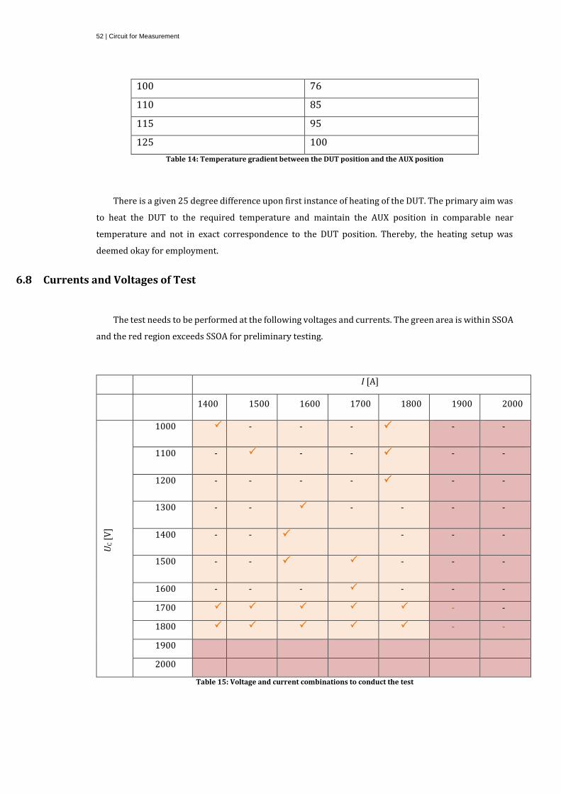
52 | Circuit for Measurement
100 76
110 85
115 95
125 100
Table 14: Temperature gradient between the DUT position and the AUX position
There is a given 25 degree difference upon first instance of heating of the DUT. The primary aim was
to heat the DUT to the required temperature and maintain the AUX position in comparable near
temperature and not in exact correspondence to the DUT position. Thereby, the heating setup was
deemed okay for employment.
6.8 Currents and Voltages of Test
The test needs to be performed at the following voltages and currents. The green area is within SSOA
and the red region exceeds SSOA for preliminary testing.
I [A]
1400 1500 1600 1700 1800 1900 2000
UC [
V]
1000 - - - - -
1100 - - - - -
1200 - - - - - -
1300 - - - - - -
1400 - - - - -
1500 - - - - -
1600 - - - - - -
1700 - -
1800 - -
1900
2000
Table 15: Voltage and current combinations to conduct the test

53

54 | Comments on the observed measurements
Chapter 7
Observed measurement
7 Comments on the observed measurements
The DUT was setup as discussed in Chapter 6. When the DUT was subjected to the pulse tests, the
turn-on di/dt turned out to be much more than expected near nominal rating of the device (1500A-1800A
@1800V). After slower driving and few more tests, the gate protection mechanisms had to be overridden
for continued functioning. The tests began with room temperatures. Unusual turn-on was observed in
the Trench device. The device was swapped to planar gate to verify if the phenomenon was only from the
trench. It was confirmed to be so. Testing was continued with varied values of current driving for turn-
on and temperatures. The causing phenomenon for this effect was found out and the necessary
modification for the gate units is suggested.
7.1 Reduction of Gate driving currents
When the testing of Trench Device began at lower levels of voltages and currents, it was observed
that the turn-on process was relatively fast. Hence, the need for reduction of turn on speed was decided
on. The reason for such a fats turn-on was point traced to very high gate turn on current (approximately
13A). For a safe turn on, the required turn-on current was calculated to be just 4A.
This was attributed to the reason for the Gate Unit’s feature of initial state analysis of the DUT and
programmed decision factor of 13A.
To override this, 3 current sources ( say, I2, I3 and I4) from the GU was removed and modified for a
constant 2A source from I1.

55
Figure 29: Preliminary runs of the turn-on.
Figure 30: Oscillogram showing the current source switch overs during turn-off.

56 | Unknown Oscillations
Chapter 8
Unknown Oscillations and Issue speculations
8 Unknown Oscillations
Upon further increasing the DUT voltage (hence the effective di/dt of the turn-on), an unusual turn-
on phenomenon was noticeable. The turn-on is characterized by a distinct peak midway through the
turn-on, dips with a flat to negative di/dt (depending on the voltage level, see Table 17) and then
proceeds to rise into the overshoot region of the diode and falls back as any common switch-diode SPT
setup in an inductive commutation configuration. This is termed as the turn-on notch/dip/kink
interchangeably.
The turn-on exhibits two distinct di/dt at these two stages. The initial one being faster than the latter.
Figure 31: DUT Current and Voltage are depicted here. The turn-on exhibits a certain anomaly which is termed as turn-on notch/dip/’kink’ interchangeably. Voltage and current levels not depicted as this phenomenon varies across the ranges and is not unique to this level.
8.1 Discussions on the oscillations
The oscillations were suspected to be caused by one of the many mentioned cases bellow. The
phenomenon can be translated as momentary increase in the channel resistance of the DUT. However,
this increase in channel resistance of the DUT can be caused either from the gate side or by the collector-

57
emitter channel itself due to unconventional carrier behavior (in perspective of time) due to change in
the gate-structure.
8.1.1 Gate side Causes:
a) The external di/dt limiter
A few capacitors are paralleled to the DUT’s gate before the device reaches the threshold voltage.
This is done to keep the turn-on DUT di/dt in check (in reality, the rate of gate-emitter voltage rise). At
faster di/dt-s these capacitors have the possibility to load the actual capacitance exhibited by the DUT’s
gate. Hence, there might be a temporary loading effect from these capacitors. The charges could be
diverted onto these capacitors. The charges could exhibit a negative flow relative to the DUT’s gate and
then could increase the channel resistance by the momentary charge extraction from the gate around the
threshold region of the device. However, such a phenomenon should be a first for the Trench Gate
strcture. The effect of Cge and Cgc has studied in in section 5.4 and 5.5 in this study [19] but does not seem
to predict it. Other studies [20][21][22] that modelled the capacitance does not seem to predict this
phenomenon aswell.
b) Gate side stray inductance:
Significant capacitance is observed when the DUT is seen in a thevenin equivalence. The possibility
of an increased inductance on the gate connectors/leads can easily allow for resonance on the gate side
that could pull the gate voltage down. However the gate voltage is strongly clamped and driven by a
constant current source. Effect of internal resonance will be hard to trace in such time scales and
capacitive currents could be difficult to measure due to a PCB outlay of the circuit. This could be
investigated as a further study for the trench devices.
8.1.2 Device side causes:
a) Emitter stray inductance:
If the module is not optimized in its build, it could be a limiting factor in the operation of the switch.
The stray inductance is extremely important a factor in these time scales. Hitachi in their ongoing
proceedings have managed to reach 40-50% increase in device performances by working on the module
optimization alone.
The effect of emitter side inductance can be hypothesized as follows. During very high di/dt of the
DUT current the emitter side voltage can raise if inductance is not kept in check. This effectively brings

58 | Unknown Oscillations
down the gate-emitter voltage. This is a negative feedback effect and can prove a limitation to such a turn
on as tried in the testing. However, the same negative feedback can prove to be useful for protection (self-
stabilization) if the device exhibits unsafely fast turn-on. The reduction in effective Vge could be a useful
aspect here.
b) Semiconductor speculations:
It is very much possible to have the semiconductor construction deviated from the
requirement/optimized template for the IGBT. The difference in current slopes during turn on could be
because of the mismatch and widely off time constants associated with the MOS channel and the main
channel. As the trench has a current flow parallel to that of the MOS channel flow, unlike a planar, the
main channel current can have an influence in the control channel. In thevenin equivalents, all these
phenomena can be back modelled as increased junction capacitances with current and voltage dependent
models. This can be dealt in a different perspective from the CHSEM.
Testing on voltage/current combinations. Investigation if the dip is from saturation effects.
For a fixed voltage level, the dip appears proportionally to the current value as exhibited in the table
DUT
Voltage
(V)
DUT
Current
(I)
di/dt –
section 1
(kA/us)
di/dt –
section 2
(kA/us)
dv/dt
(kV/us)
Peak
Level
(A)
Bump
level
(A)
1000 500 3,2 0,8 0,6 675 -
1480 500 4,63 0,9 0,8 1000 -
1420 950 4,34 1 0,84 1320 1000
1300 1330 3,7 1,65 0,76 2000 1000
1538 1543 4,74 1,70 0,87 2260 1000
Table 167: Current notch and current dependence
However, for lower voltages and higher currents, the appearance of the dip is much lower in current
levels. This could be pointed out to effective device saturation in appropriate levels -The presence of
lower levels of barriers for current establishment in the n-drift region.

59

60 | Observed Test Results
Chapter 9
Optimal Driving of the Trench and Issue Solution
The following chapter discusses the action adopted for the hypothesis discussed and finally suggests
an optimal driving solution for the trench sample obtained. The issue rectification is undertaken and the
hypothesis is proved.
9 Observed Test Results
The hypothesis of the gate being loaded by the capacitors was tested.
The test immediately revealed improved switch-on performance on decreasing steps of external
di/dt limiters or capacitors.
Test 1:
1800V/1880A
990nF and 2.7A
Turn-on di/dt = 1,8kA/us
Figure 32: Turn-on exhibiting a current dip in discussion.

61
Test 2:
1800V/1800A
660nF and 2.7A
Turn-on di/dt = 6,4kA/us
Figure 33: Reduced current dip relative to the turn-on in Fig. 32
Test 3:
1800V/1800A
330nF and 2.7A
Turn-on di/dt = 6kA/us
Figure 34: Reduced current dip relative to the the turn-on in Fig. 32 and Fig. 33

62 | Observed Test Results
The turn on di/dit is also reduced by 400A/us indicating an effective utilization of the charging
capacitive current instead of external diversion from the external gate snubbers.
The second hypothesis of trying to slow down the driving in order to give enough times for ‘the
channel to open up’ for conduction was tested. In this test the device seemed to perform even more
poorly.
The current source (I1) was reduced from 2.7A to 2A. The device naturally turned on slower, but
also, the dip on the turn on was even more pronounced. The device goes for a partial turn off and then
starts conduction again. This directly gives an indication that the gate is short of charges for the proper
turn-on.
SLOWER DRIVING 2.0 A / 990nF (problem is even more pronounced)
Figure 35: Worsened current dip. See Fig. 32-34

63

64 | Summary of Work Done
Chapter 10
Discussion and Summary
10 Summary of Work Done
1) The Trench IGBT sample that was obtained was studied in terms of the gate driving requirement.
2) A motivating loss calculation was performed to prove that trench technology could be a viable
and effective candidate for the semiconductor switch being employed in upcoming HVDC
projects in relation to ABB’s template of HVDC convertors.
3) After a hypothesis was formed about the unusual turn-on behavior of the trench, it was tested
and proved.
4) A suitable modification was then suggested to steer the device to a minimal loss operation.
10.1 Further studies
1) The behavior of the trench-technology bordering the SOA can be studied. Short circuit studies
can be performed to understand its dynamics with the type of driving employed at HVDC for
relevant interest.
2) Latching of the IGBT can be studied and benchmarked against the planar technology.
3) Dynamic driving can be looked into for employment. The reference voltage levels employed for
the voltage sharing feature of the gate units can be modified to drive the device dynamically.
Meaning, the IGBT can be turned on/off at different speeds within the stages of turn on turn-off.
4) Since the driving calls for reduced gate side capacitance, Rg based driving might be even more
effective. However, the need for a faster driving in about 70 percentage of turn-on (/off) event
requires further investigation.
5) The limiting factor of the diode can be investigated in detail. Example includes the employment
of a silicon-carbide technology for the diode (such as Hitachi modules)

65
10.2 Conclusion
1) Dynamic driving with multiple (at least two) current sources is suggested to be maintained to
rectify capacitance issue.
2) The trench technology as a BIGT of higher voltage class (greater than 3.3 kV) will prove
extremely advantageous for MMC topology such as Generation 5 instead of fast-switching based
topologies.
3) No drastic need for new gate units with regards to what has been studied. Here is an opportunity
for GU cost reduction.
4) Remove external di/dt limiters in GU. Simplify gate unit. Here is an opportunity for GU cost
reduction.
5) Reduce the number of current sources to two. . Here is an opportunity for GU cost reduction.


References |
References
[1] K. Eriksson, “HVDC Light™ and development of Voltage Source Converters,” ABB. [Online]. Available: https://library.e.abb.com
[2] K. Eriksson, "It’s time to connect with offshore wind supplement," [Online]. Available:
https://library.e.abb.com
[3]"Technical description of HVDC Light® technology," [Online]. Available:
http://www.tdproducts.com/files/36371732.pdf.
[4] N. Iwamuro and T. Laska, “IGBT History, State-of-the-Art, and Future Prospects,” Electron Devices, IEEE
Transactions on, vol. 64, no. 3, pp. 741–752, 2017.
[5] B. J. Baliga, Fundamentals of Power Semiconductor Devices. 2008.
[6] Raghavendra S. Saxena and M. Jagadesh Kumar, "Trench Gate Power MOSFET: Recent Advances and Innovations", Advances in Microelectronics and Photonics,(Ed., S. Jit), Chapter 1, Nova Science Publishers, Inc. 400 Oser Avenue, Suite 1600, Hauppauge, NY 11788, USA, pp:1-23, 2012
[7] H. Chang, B. Baliga, J. Kretchmer, and P. Piacente, “INSULATED GATE BIPOLAR TRANSISTOR (IGBT)
WITH A TRENCH GATE STRUCTURE.,” Technical Digest - International Electron Devices Meeting, pp. 674–
677, 1987.
[8] T. Kushima, K. Azuma, Y. Nemoto, Y. Koike, and K. Saito, “1800A/3.3kV IGBT module using advanced
trench HiGT structure and module design optimization,” PCIM Europe Conference Proceedings, pp. 346–
353, 2014.
[9] Wang, Wu, Jones, Dai, and Liu, “Challenges and trends of high power IGBT module packaging,”
Transportation Electrification Asia-Pacific (ITEC Asia-Pacific), 2014 IEEE Conference and Expo, pp. 1–7,
2014.
[10] Z. Shen, F. Zhang, L. Tian, G. Yan, Z. Wen, W. Zhao, L. Wang, X. Liu, G. Sun, and Y. Zeng, “Optimized P-
emitter doping for switching-off loss of superjunction 4H-SiC IGBTs,” Wide Bandgap Semiconductors
China (SSLChina: IFWS), 2016 13th China International Forum on Solid State Lighting: International
Forum on, pp. 1–5, 2016.
[11] A. Kopta, M. Rahimo, U. Schlapbach, N. Kaminski, and D. Silber, “Limitation of the short-circuit
ruggedness of high-voltage IGBTs,” Power Semiconductor Devices & IC's, 2009. ISPSD 2009. 21st
International Symposium on, pp. 33–36, 2009.
[12] E. R. Motto, J. F. Donlon, H. Takahashi, M. Tabata, and Iwamoto, “Characteristics of a 1200 V PT IGBT
with trench gate and local life time control,” Conference Record - IAS Annual Meeting (IEEE Industry
Applications Society), vol. 2, pp. 811–816, 1998.
[13] S. Linder et al., “Soft Punch Through (SPT) – Setting new Standards in 1200V
IGBT”, www.mena.abb.com.
[14] ] M. Rahimo et al., “Next Generation Planar IGBTs with SPT+ Technology”, www.mena.abb.com.
[15] Ma Rongyao, “Carrier stored trench-gate bipolar transistor with p-floating layer,” Journal of
Semiconductors, vol. 31, no. 2, p. 5, 2010.

| References
[16] D. Lammers, "POWER STRUGGLE," [Online]. Available:
http://www.appliedmaterials.com/nanochip/nanochip-fab-solutions/december-2013/power-struggle.
[17] E. J. Ng, C. F. Chiang, Y. Yang, V. A. Hong, C. H. Ahn and T. W. Kenny, "Ultra-high aspect ratio trenches in
single crystal silicon with epitaxial gap tuning," 2013 Transducers & Eurosensors XXVII: The 17th
International Conference on Solid-State Sensors, Actuators and Microsystems (TRANSDUCERS &
EUROSENSORS XXVII), Barcelona, 2013, pp. 182-185.
[18] Deviny, Ian, Luo, Haihui, Xiao, Qiang, Yao, Yao, Zhu, Chunlin, Ngwendson, Luther-King, Xiao, Haibo,
Dai, Xiaoping, and Liu, Guoyou, “A novel 1700V RET-IGBT (recessed emitter trench IGBT) shows record
low VCE(ON), enhanced current handling capability and short circuit robustness,” Power Semiconductor
Devices and IC's (ISPSD), 2017 29th International Symposium on, pp. 147–150, 2017.
[19] Zhou, L. (2009) Mixed-mode Circuit and Device Simulations of IGBT with Gate Unit Using Synopsys Sentaurus Device. Göteborg : Chalmers University of Technology
[20] J. Yang and M. Norgren, “Modeling of HVDC IGBT in Pspice: Serving an ultimate goal for converter
station EMC studies,” 2015.
[21] Z. Norouzian, L. Landin, E. Nilsson, and H. Pettersson, “Modeling of IGBT Modules with Parasitics
Elements Evaluation,” 2013.
[22] Boehmer, Schumann, and Eckel, “Effect of the miller-capacitance during switching transients of IGBT
and MOSFET,” Power Electronics and Motion Control Conference (EPE/PEMC), 2012 15th International,
pp. LS6d.3–1-LS6d.3–5, 2012.

69
TRITA-EECS-EX-2018:658
www.kth.se