Embed Size (px)
Citation preview
UNIVERSITY of CALIFORNIA
SANTA CRUZ
INVESTIGATION OF SILICON SENSOR STRIP NOISE ON LONGLADDERS
A thesis submitted in partial satisfaction of therequirements for the degree of
BACHELOR OF SCIENCE
in
PHYSICS
by
Sean C. H. Crosby
10 June 2009
The thesis of Sean C. H. Crosby is approved by:
Professor Bruce SchummTechnical Advisor
Professor David P. BelangerThesis Advisor
Professor David P. BelangerChair, Department of Physics
Copyright c© by
Sean C. H. Crosby
2009
Abstract
Investigation of Silicon Sensor Strip Noise on Long Ladders
by
Sean C. H. Crosby
The equivalent charge noise for long ladder silicon strip sensors is examined in this paper. It is
found to deviate from standard estimation formulae. To simulate a long ladder detector many
strips on a single detector were connected in a serpentine arrangement. The equivalent charge noise
measured for this long ladder detector was much lower than expected, despite the rigorous estimation
techniques used involving shaper and amplifier constants. These results suggest that there are effects
not yet understood for long ladder silicon sensors.
iv
Contents
List of Figures v
Dedication vi
Acknowledgements vii
1 Motivation 1
2 Background 42.1 Silicon Sensors . . . . . . . . . . . . . . . . . . . . . . . . . . . . . . . . . . . . . . . 42.2 Noise . . . . . . . . . . . . . . . . . . . . . . . . . . . . . . . . . . . . . . . . . . . . . 6
3 Materials and Method 103.1 Readout Electronics . . . . . . . . . . . . . . . . . . . . . . . . . . . . . . . . . . . . 103.2 Noise Measurements . . . . . . . . . . . . . . . . . . . . . . . . . . . . . . . . . . . . 113.3 Pulse Shaping . . . . . . . . . . . . . . . . . . . . . . . . . . . . . . . . . . . . . . . . 133.4 The Sensor . . . . . . . . . . . . . . . . . . . . . . . . . . . . . . . . . . . . . . . . . 153.5 The Service Board . . . . . . . . . . . . . . . . . . . . . . . . . . . . . . . . . . . . . 16
4 Results and Analysis 19
5 Conclusion 245.1 Further Studies . . . . . . . . . . . . . . . . . . . . . . . . . . . . . . . . . . . . . . . 25
Bibliography 26

v
List of Figures
1.1 Illustration of proposed SID detector . . . . . . . . . . . . . . . . . . . . . . . . . . . 2
2.1 AC-biased silicon sensor illustration . . . . . . . . . . . . . . . . . . . . . . . . . . . 5
3.1 Instrument setup diagram . . . . . . . . . . . . . . . . . . . . . . . . . . . . . . . . . 103.2 S-curves for different input charges . . . . . . . . . . . . . . . . . . . . . . . . . . . . 123.3 Noise and Gain Measurements . . . . . . . . . . . . . . . . . . . . . . . . . . . . . . 123.4 Normalized Shaper Output Signal . . . . . . . . . . . . . . . . . . . . . . . . . . . . 143.5 Service Board Diagram . . . . . . . . . . . . . . . . . . . . . . . . . . . . . . . . . . . 17
4.1 Noise measured for different values of capacitance using the LTSFE chip and setupdescribed in section 3.1. Shaper Current set to 300nA . . . . . . . . . . . . . . . . . 20
4.2 Strip Chain Noise Measurement and Estimation . . . . . . . . . . . . . . . . . . . . . 224.3 Strip Chain Noise Percent Source Estimation . . . . . . . . . . . . . . . . . . . . . . 234.4 Strip Chain Noise Absolute Noise Estimation . . . . . . . . . . . . . . . . . . . . . . 23
5.1 Example of RC network . . . . . . . . . . . . . . . . . . . . . . . . . . . . . . . . . . 24

vi
To my Parents, for always supporting me not matter what my interest is.
To my Brother, who will always listen.

vii
Acknowledgements
I would like to thank;
My thesis advisor, Bruce Schumm. Without your support I would have never finished this
paper or got to work on such an interesting project.
Vitality Fadeyev. Without your help, support and vast knowledge and know-how none of
this would be possible.
Forest Martinez-McKinney. For many countless and beautiful wirebonds, and lots of
technical advice.
Max Wilder. For guidance and very practical help.
LTSFE2 team. For making it a fun and interesting time.
1
1 Motivation
The International Linear Collider (ILC) will be the worlds highest energy electron-positron
collider. It will accelerate electrons and positrons to produce center-of-mass energies of 500GeV.
The ILC will be used to precisely study new forces and matter states discovered at the Large Hadron
Collider (LHC). It is currently in the design phase, and the community has not yet decided on a
detector concept. Of the three proposed concepts, in particular, the SID concept utilizes solid-state
silicon tracking, and a silicon-tungsten sampling calorimeter. The detector will be composed of many
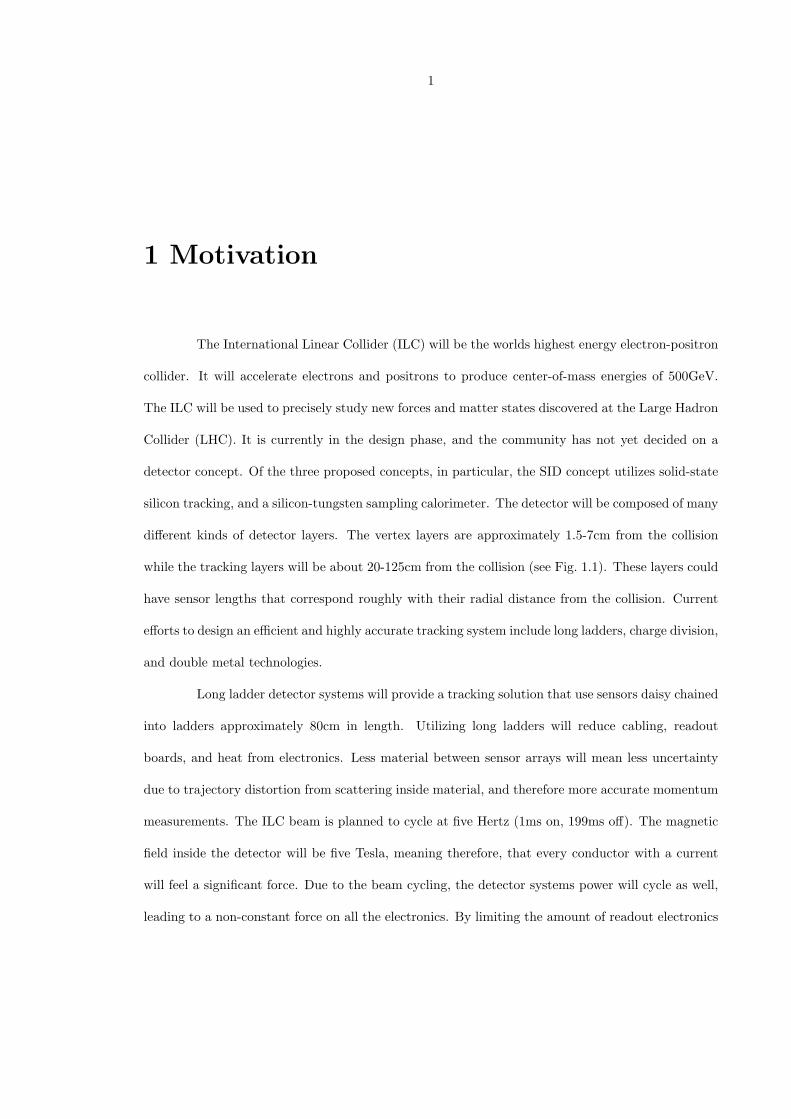
different kinds of detector layers. The vertex layers are approximately 1.5-7cm from the collision
while the tracking layers will be about 20-125cm from the collision (see Fig. 1.1). These layers could
have sensor lengths that correspond roughly with their radial distance from the collision. Current
efforts to design an efficient and highly accurate tracking system include long ladders, charge division,
and double metal technologies.
Long ladder detector systems will provide a tracking solution that use sensors daisy chained
into ladders approximately 80cm in length. Utilizing long ladders will reduce cabling, readout
boards, and heat from electronics. Less material between sensor arrays will mean less uncertainty
due to trajectory distortion from scattering inside material, and therefore more accurate momentum
measurements. The ILC beam is planned to cycle at five Hertz (1ms on, 199ms off). The magnetic
field inside the detector will be five Tesla, meaning therefore, that every conductor with a current
will feel a significant force. Due to the beam cycling, the detector systems power will cycle as well,
leading to a non-constant force on all the electronics. By limiting the amount of readout electronics
2
Figure 1.1: An illustration of a single quadrant of the SID detector design. Length scale shownabove is in meters.[2]
this periodic ”hammering” force will be reduced. The reduction of material will also produce more
accurate calorimeter measurements due a reduced amount of photon conversion.
While a long ladder detector system provides many solutions, the accuracy of signal mea-
surements is not well known. As readout strip length increases, so does the strip capacitance and
resistance. Because the tracking system needs to be extremely accurate, very narrow strips with
very fine pitches are used. The strips themselves are approximately 7um wide, and their pitch (the
distance between two strips) is 50um. These narrow strips have a large resistance ( 3KOhms for
80cm) leading to a potentially large readout noise. This noise contribution from strip resistance
does not increase linearly with length. In fact, the noise contribution is expected to increase as
length(3/2). This can be seen from the noise estimation equation, Eq. 1.1, derived Helmuth Spieler
[1]. Q is noise in electrons. Id, Rb, Rs, and C are sensor characteristics referring respectively to
leakage (quiescent) current, bias resistance, strip resistance, and strip capacitance. The shaping
factors Fi and Fv, and are of order one and the time constant τ is a measure of pulse shaping. These
are discussed in section 3.3.
3
Q2 = Fiτ(2eId +4kTRb
+ i2na) +FvC
2
τ(4kTRs + e2na) + 4FvAfC2 [SI Units] (1.1)
As seen in Eq. 1.1 the strip resistance term, Rs is multiplied by C2. Because resistance and
capacitance are both proportional to length, Q2 ∼ l3 or Q ∼ l3/2. This non-linearity is my focus of
concern. As the signal-to-noise ratio is critical to understanding the achievable positional resolution
for high energy particles, the question of whether this approximate equation is valid at long length
scales is very important. This is where an experimental study is needed.

4
2 Background
2.1 Silicon Sensors
Silicon sensors are used to detect ionizing particles. They are used in a variety of set-
tings including radiation and photon detection. Because they are solid state devices that work at
high speed they can be very accurate, they are ideal candidates for detection systems in particle
accelerators.
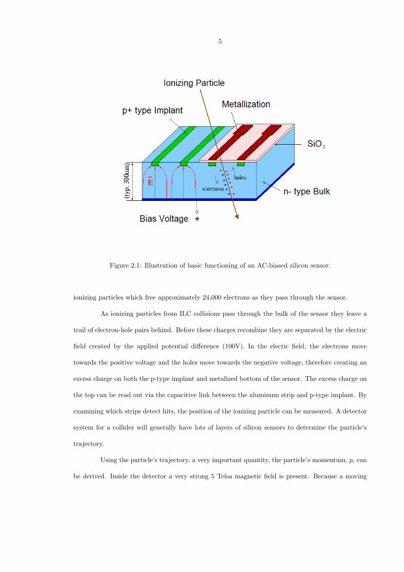
The common AC-coupled sensor will be the focus of my study. It can be described in
simplest terms a diode. Commonly n-type silicon is used for the bulk of the sensor, and p-type
silicon is implanted in long strips on the bulk surface (see Fig. 2.1). The bulk will get a metalization
layer on its backside, and the p-type strips will get an insulating layer of silicon oxide on their
topside. Aluminum strips will be placed on top of the silicon oxide creating a capacitor with the
p-type implant. As a protective measure, a passivation layer is deposited on top of the entire sensor
leaving exposed pads for wire bonding connections.
By applying a positive potential to the backside metalization and connecting the p-type
implants to ground via a bias resistor, a reverse bias is applied to this diode. The depletion region
will increase as a greater potential is applied. If a large enough potential is applied the entire n-type
bulk will be completely depleted, and therefore free of any charge carriers. As shown in Fig. 2.1, an
electric field is generated inside the bulk by the potential difference. Because most sensors deplete at
or before 100V, this is the bias voltage used for my studies. This configuration is ideal for detecting
5
Figure 2.1: Illustration of basic functioning of an AC-biased silicon sensor.
ionizing particles which free approximately 24,000 electrons as they pass through the sensor.
As ionizing particles from ILC collisions pass through the bulk of the sensor they leave a
trail of electron-hole pairs behind. Before these charges recombine they are separated by the electric
field created by the applied potential difference (100V). In the electic field, the electrons move
towards the positive voltage and the holes move towards the negative voltage, therefore creating an
excess charge on both the p-type implant and metalized bottom of the sensor. The excess charge on
the top can be read out via the capacitive link between the aluminum strip and p-type implant. By
examining which strips detect hits, the position of the ionizing particle can be measured. A detector
system for a collider will generally have lots of layers of silicon sensors to determine the particle’s
trajectory.
Using the particle’s trajectory, a very important quantity, the particle’s momentum, p, can
be derived. Inside the detector a very strong 5 Telsa magnetic field is present. Because a moving
6
charged particle in a magnetic field will feel a force perpendicular to its velocity, the ionizing particles
from collisions will follow a curved trajectory as they leave the detector. The momentum can be
determined by measuring the radius of this curvature of the trajectory as seen below.
r[m] =p ∗ c300B
[MeV
Tesla
](2.1)
Here, r is radius, p is momentum, c is the speed of light, and B is the magnetic field.[3]
The ILC will be designed to examine very high energy particles that, despite the strong
magnetic field, will have very large radii of curvature. The ability to measure this slight curvature is
crucial in making accurate momentum measurements. Using a strip pitch of 50um, position can be
determined to better than 10um by examining the distribution of charge left by the ionizing particle.
This ability to measure this charge signal accurately is essential to achieve a high position resolution
that results in an accurate momentum measurements.
2.2 Noise
Electronic noise is random fluctuations in the amplified signal due to a variety of effects.
These fluctuations obscure the signal and can degrade the quality of the data provided by the sensor.
The most important influence of noise is the signal-to-noise ratio. This ratio provides a figure of
merit used to determine the amount of information one can derive from a signal.
Electronic noise can be thought of as fluctuations in current. This leads to two statistically
independent sources: he velocity fluctuations of electrons, and the number fluctuations of electrons.
Velocity fluctuations come from thermal motion of atoms in the conducting material. This jostling
yields a large dispersion of velocities. The number fluctuation in electrons is due to many different
sources such as thermionic emission or carrier generation and recombination.
The primary focus of this experiment will be thermal noise, but to understand our noise
measurements, all noise sources of our silicon sensor must be understood and approximated. Thermal
noise, commonly referred to as ”Johnson noise”, arises due to velocity fluctuations in resistors. In the

7
voltage regime, or for series resistance, the noise density is proportional to resistance (See Eq. 2.2).
In the current regime, or for parallel resistance, the spectral noise density is inversely proportional to
resistance (See Eq. 2.3). Spectral noise density is the noise measured per unit of bandwidth. These
equations are derived for example by Helmuth Spieler[1].
e2 = 4kTR (2.2)
i2 =4kTR
(2.3)
Shot noise is another important noise source arising due to number fluctuations. Shot noise
arises due to charge carriers injected independently of one another. Because the silicon sensor is
essentially a diode it is subject to dark current. Dark current is a small reverse current through
a diode due to quantum fluctuations arising from the Boltzmann distribution of carrier energies.
This Dark current is genearlly characterized as ’leakage’ current. These fluctuations are increased
by the large reverse bias voltage applied to the sensor and these release times generally follow a
Poisson distribution. This leads to a spectral noise density proportional to the current(I) generated
by additional carriers (see Eq. 2.4).
i2 = 2eI (2.4)
A third noise source, commonly called 1/f noise, occurs when fluctuations are not random.
Carrier trapping and release is a good example of this noise type. Carriers are trapped with various
release lifetimes. An effectively infinite, uniformly distributed set of trapping times yield a power
density inversely proportional to frequency (f). Because the noise contribution is larger when f is
small, this is sometimes called low frequency noise.
To estimate the noise from the sensor, all these noise sources must be combined and inte-
grated over the entire frequency spectrum. Derivations in [1] show the noise measured for a sensor of
characteristics Id, Rb, Rs, and C and amplifier characteristics ina, ena, Af . This derivaiton is shown
by Eq. 1.1 and here as Eq. 2.5 for convenience. The shaping factors Fi and Fv, and the time con-
stant, τ , come from the shaping characteristics of the amplifier used to read out the sensor. They
8
are discussed in section 3.3.
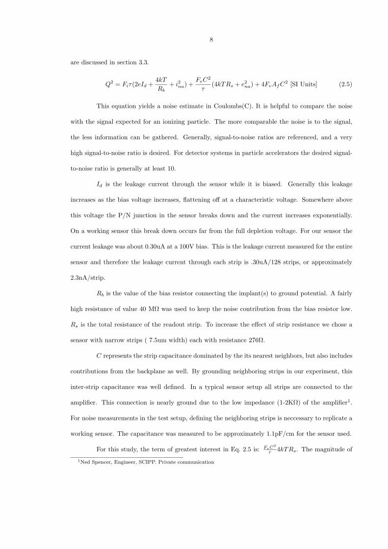
Q2 = Fiτ(2eId +4kTRb
+ i2na) +FvC
2
τ(4kTRs + e2na) + 4FvAfC2 [SI Units] (2.5)
This equation yields a noise estimate in Coulombs(C). It is helpful to compare the noise
with the signal expected for an ionizing particle. The more comparable the noise is to the signal,
the less information can be gathered. Generally, signal-to-noise ratios are referenced, and a very
high signal-to-noise ratio is desired. For detector systems in particle accelerators the desired signal-
to-noise ratio is generally at least 10.
Id is the leakage current through the sensor while it is biased. Generally this leakage
increases as the bias voltage increases, flattening off at a characteristic voltage. Somewhere above
this voltage the P/N junction in the sensor breaks down and the current increases exponentially.
On a working sensor this break down occurs far from the full depletion voltage. For our sensor the
current leakage was about 0.30uA at a 100V bias. This is the leakage current measured for the entire
sensor and therefore the leakage current through each strip is .30uA/128 strips, or approximately
2.3nA/strip.
Rb is the value of the bias resistor connecting the implant(s) to ground potential. A fairly
high resistance of value 40 MΩ was used to keep the noise contribution from the bias resistor low.
Rs is the total resistance of the readout strip. To increase the effect of strip resistance we chose a
sensor with narrow strips ( 7.5um width) each with resistance 276Ω.
C represents the strip capacitance dominated by the its nearest neighbors, but also includes
contributions from the backplane as well. By grounding neighboring strips in our experiment, this
inter-strip capacitance was well defined. In a typical sensor setup all strips are connected to the
amplifier. This connection is nearly ground due to the low impedance (1-2KΩ) of the amplifier1.
For noise measurements in the test setup, defining the neighboring strips is neccessary to replicate a
working sensor. The capacitance was measured to be approximately 1.1pF/cm for the sensor used.
For this study, the term of greatest interest in Eq. 2.5 is: FvC2
τ 4kTRs. The magnitude of
1Ned Spencer, Engineer, SCIPP. Private communication

9
this term is determined by the strip resistance and capacitance. Its effect on long ladders may be
severe due to its nonlinear dependence on strip length. Strip resistance and capacitance are both
proportional to strip length(l) yielding a relationship to noise: Q2 ∼ l3 or Q ∼ l3/2. Therefore as
strip length increases this term becomes the dominating noise source, and is my primary concern in
this study.
In prior experiments with short or wide strip sensors, the noise generated by strip resis-
tance(strip noise) was not a large consideration due to its small effect. Exact shaper constants,
Fi and Fv, had small effects on the total noise. Initially I naively used this simplified equation
based on a CR-RC shaper with shaper constants, Fv = Fi = .924, linearily combined with Eq. 2.7.
Equation 2.7 represents strip noise, and was estimated with the same CR-RC shaper constants.
Q2 = 12[
e2
nA ∗ ns
]Idτ + 6 ∗ 105
[e2kΩns
]τ
Rb+ 3.6 ∗ 104
[e2ns
(pF )2(nV )2/Hz
]e2nC2
τ(2.6)
Q2 =Fv4kTRsC2
τ[SI Units] (2.7)
For single strip length measurements this combined equation (added in quadrature) agreed very well.
Only when longer strip lengths were examined, did the importance of Eq. 2.5 become apparent. Prior
to examining Eq. 2.5 I was unaware that the shaping factors had such a large effect at long strip
lengths. Therefore, to achieve better estimates for long ladder sensor chains, amplifier characteristics
will need to be well known. These characteristics are discussed in section 3.3.
10
3 Materials and Method
3.1 Readout Electronics
Reading out the excess charge generated on the strips of the sensor by an ionizing particle
requires well designed amplification and shaping electronics. Because the charge is very small,
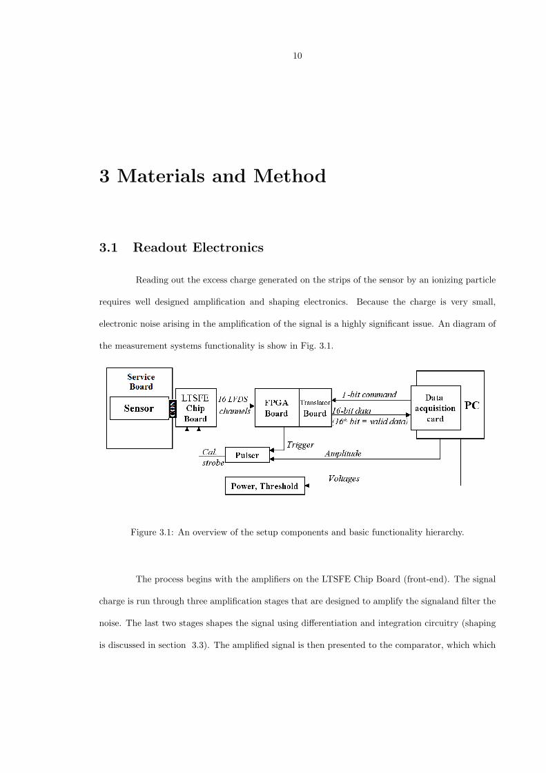
electronic noise arising in the amplification of the signal is a highly significant issue. An diagram of
the measurement systems functionality is show in Fig. 3.1.
Figure 3.1: An overview of the setup components and basic functionality hierarchy.
The process begins with the amplifiers on the LTSFE Chip Board (front-end). The signal
charge is run through three amplification stages that are designed to amplify the signaland filter the
noise. The last two stages shapes the signal using differentiation and integration circuitry (shaping
is discussed in section 3.3). The amplified signal is then presented to the comparator, which which

11
provides an output signal (”hit”) when its input exceeds a pre-defined threshold. These hits are
then sent in the low voltage differential signal (LVDS) standard to the FPGA board. Hits are read
out through the connecting board to a data acquisition card on the PC (see Fig. 3.1).
Power and threshold voltages are supplied to the front end board by a stack of power
supplies. Because it is not easy to direct ionizing particles at the sensor strips with high spatial
precision, a pulser is used to produce the charge on readout lines. A 1pF capacitor is connected
serially in line to the reaout strip to transform the voltage signla provided by the pulser into a charge.
These power supplies and pulser are controlled by the PC using the General Purpose Interface Bus
(GPIB). The pulser is also triggered by the FPGA (see Fig. 3.1).
3.2 Noise Measurements
The occupancy method was used to make noise measurements in this study. The idea
behind this method is the generation of S-curves. An S-curve is plot of occupancy versus threshold.
Given a particular threshold voltage established by a power supply, a set number of pulses are
generated and then readout through the comparator. The FPGA then sends the number of hits
recorded at that threshold to the comparator. This number of hits divided by the total pulses sent
is the occupancy. Given a noiseless system, if the threshold voltage is less than the voltage of the
input pulse, we would expect to record the same number of hits and pulses sent. Even in a normal
noisy setting, if the threshold is low enough, occupancy is 100%. By varying the threshold below
and above the voltage of the input pulse, an S-curve is generated (see Fig. 3.2).
The derivative of the S-curve follows a Gaussian distribution. The 50% occupancy level
corresponds to the peak of the Gaussian and the Gaussians width corresponds to the characteristic
width of the S-curve. A very steep S-Curve means a very sharp Gaussian peak and therefore a low
noise, while a shallow S-curve means a very wide Gaussian peak corresponding to high noise. The
threshold position of 50% occupancy represents the input signal measured after amplification. This
happnes, because on average, half the time noise will bring the signal below threshold and half the
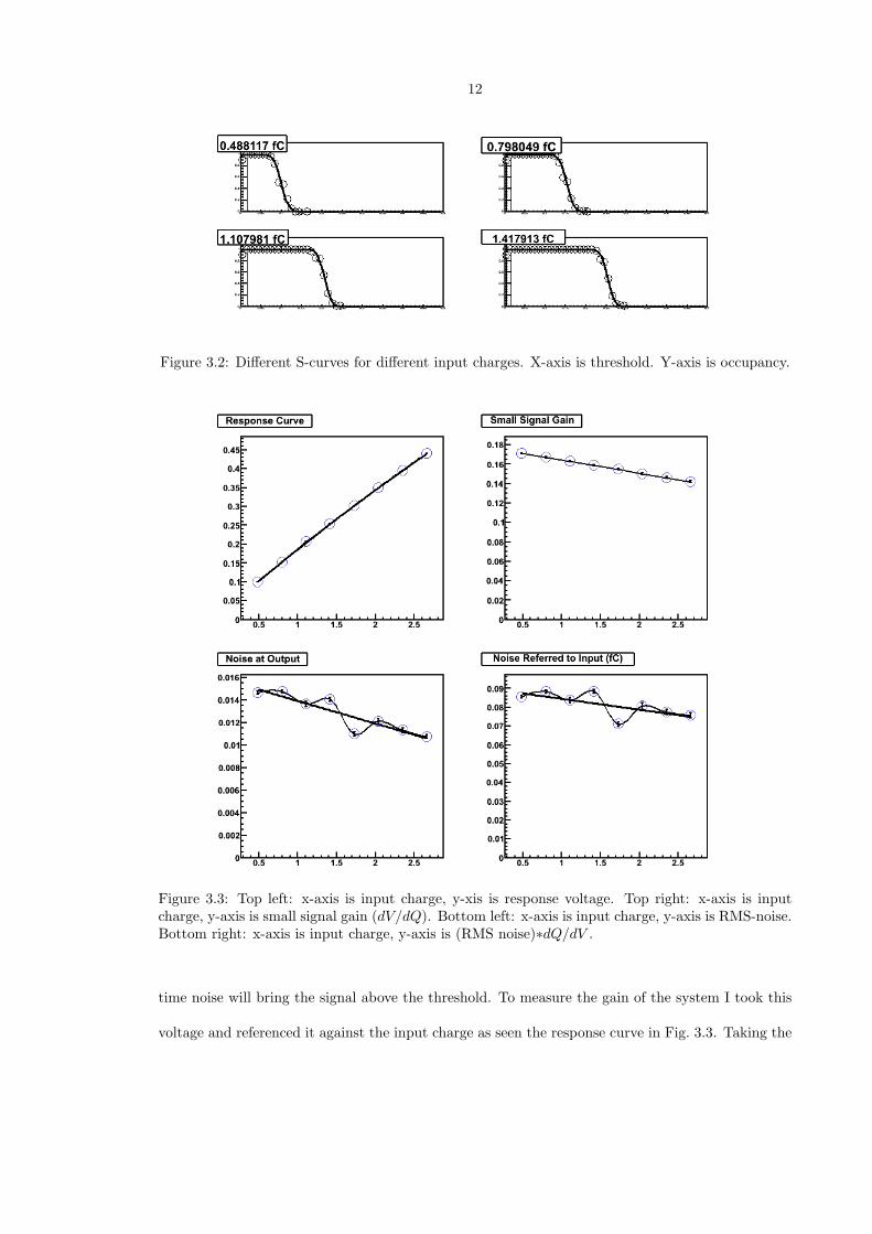
12
Figure 3.2: Different S-curves for different input charges. X-axis is threshold. Y-axis is occupancy.
Figure 3.3: Top left: x-axis is input charge, y-xis is response voltage. Top right: x-axis is inputcharge, y-axis is small signal gain (dV/dQ). Bottom left: x-axis is input charge, y-axis is RMS-noise.Bottom right: x-axis is input charge, y-axis is (RMS noise)∗dQ/dV .
time noise will bring the signal above the threshold. To measure the gain of the system I took this
voltage and referenced it against the input charge as seen the response curve in Fig. 3.3. Taking the
13
derivative of the response curve (dV/dQ) yields the small signal gain also shown in Fig. 3.3.
The noise at amplifier’s output is measured as the width of the S-curve transition. The
value plotted against the input charge is shown as Noise at Output in Fig. 3.3. To translate this value
to the noise that would have been on amplifier’s input, I divide it by the measured gain (Fig. 3.3).
It is important to vary the input charge so that the gain of the system can be observed. The LTSFE
chip was designed to have a gain that rolls off with increasing pulse heights. This is observed in the
Small Signal Gain graph in Fig 3.3.
3.3 Pulse Shaping
The primary purpose of the pulse shaper is to improve the signal-to-noise ratio by taking
advantage of the difference in frequency distribution of the noise and signal. By applying a filter
in just the frequency range of the signal, the noise in other frequency bands can be attenuated. In
order to make accurate predictions of noise, it is necessary to characterize the shaper output.
An oscilloscope is connected to a pico probe to measure the shaper output directly from the
LTSFE chip on the front-end LTSFE board. Using the oscilloscope averaging software, I obtained
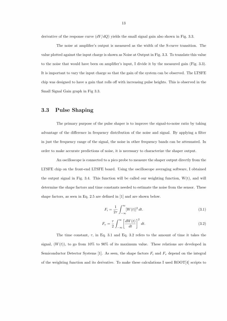
the output signal in Fig. 3.4. This function will be called our weighting function, W(t), and will
determine the shape factors and time constants needed to estimate the noise from the sensor. These
shape factors, as seen in Eq. 2.5 are defined in [1] and are shown below.
Fi =12τ
∫ ∞−∞
[W (t)]2 dt. (3.1)
Fv =τ
2
∫ ∞−∞
[dW (t)dt
]2dt. (3.2)
The time constant, τ, in Eq. 3.1 and Eq. 3.2 refers to the amount of time it takes the
signal, (W (t)), to go from 10% to 90% of its maximum value. These relations are developed in
Semiconductor Detector Systems [1]. As seen, the shape factors Fi and Fv depend on the integral
of the weighting function and its derivative. To make these calculations I used ROOT[4] scripts to
14
Figure 3.4: Averaged Shaper Signal Output as read from Oscilloscope. Shaper current was 250nAand input voltage was 1.76V. For calculation this is our weighting function W(t)
fit the weighting function, and evaluate its integral numerically1. Results are displayed in Table 3.1
Shaper 0.66V 1.32V (pulse heights)Fi 1.47 1.59Fv 0.489 0.443τ (us) 1.06 1.02
Table 3.1: Shape factors and time constants for different pulse heights. Shaping current set to 300nA
The weighting function did not varied significantly with shaper current and pulse height
used for my noise measurents; however, The shape factors estimated were very different from those
previously used bases on a simple CR-RC shaper (Fi = Fv = 1 for CR-RC shaper). These differences
proved to be important in our noise estimations. Shaper current had previously been optimized to1These ROOT scipts were written and provided by Vitaliy Fadeyev, PhD, SCIPP

15
300nA. This was confirmed by examining noise predictions for varied shaper currents. Because it is
necessary to vary the input voltage to generate S-curves, the shaping factors for these varying input
voltages must be known. By varying the input voltages and holding the shaper current constant at
300nA, weighting functions were measured, and shaping factors were calculated.
3.4 The Sensor
Selectin a sensor and determining method of examining long ladders were two critical
decisions in this experiment. The sensor selected was an improperly fabricated DC-biased sensor
originally intended for Charge Division2 studies. DC-biased sensors differ slightly from AC-biased
sensors in that the signal transfer between the implant and readout strips is different. For AC-
biased sensors, the implant strip is capacitively coupled to the readout strip, while for DC-biased
sensors, the implant strip is ohmically coupled to the readout strip. The problem in the fabrication
of these Charge Division sensors was the inclusion of a metal readout strip connected and shorting
the implant strip every 100um along its length. Readout was supposed to be achieved by connecting
just to the ends of the implant. The mistakenly placed readout strip was very thin and therefore
had the large value of resistance that is necessary to examine the strip resistance’s contribution to
noise. While these Charge Division detectors seemed ideal due to the misfabrication, the absence of
a large bias resistor and readout coupling capacitor made the service board slightly more complex
(discussed in section 3.5).
A previous attempt to measure the noise effects due to strip resistance in long ladder
detector systems used GLAST3 sensors connected in series. This attempt required many sensors
and lots of materials to shield and connect them. Unfortunately this attempt did not yield the
desired results due to the low resistance of the GLAST readout strips ( 10Ω/strip). Rather than
use many chained together sensors, the idea behind this experiment was to use many of the strips2Charge Division is another detector design intended for the ILC that takes advantage of the long cycling time by
reading out sensors from both ends. By measuring the distribution of charge on both ends a longitudinal measurementcan be made
3GLAST sensors were small scale test structures of the sensors used in the GLAST/FERMI x-ray satellite
16
on one sensor. The Charge Division sensor had 128 readout strips available at a pitch of 50um.
This sensor was ideal not just due to the high resistance of its readout strips, but also due to its
geometric similarity to the sensors intended for the long ladder SID design. By connecting the strips
in a serpentine arrangement, a much longer sensor can be simulated. With such a large number of
readout strips, the only constraint is the ability of the service board to interface to the small 50um
pitch.
3.5 The Service Board
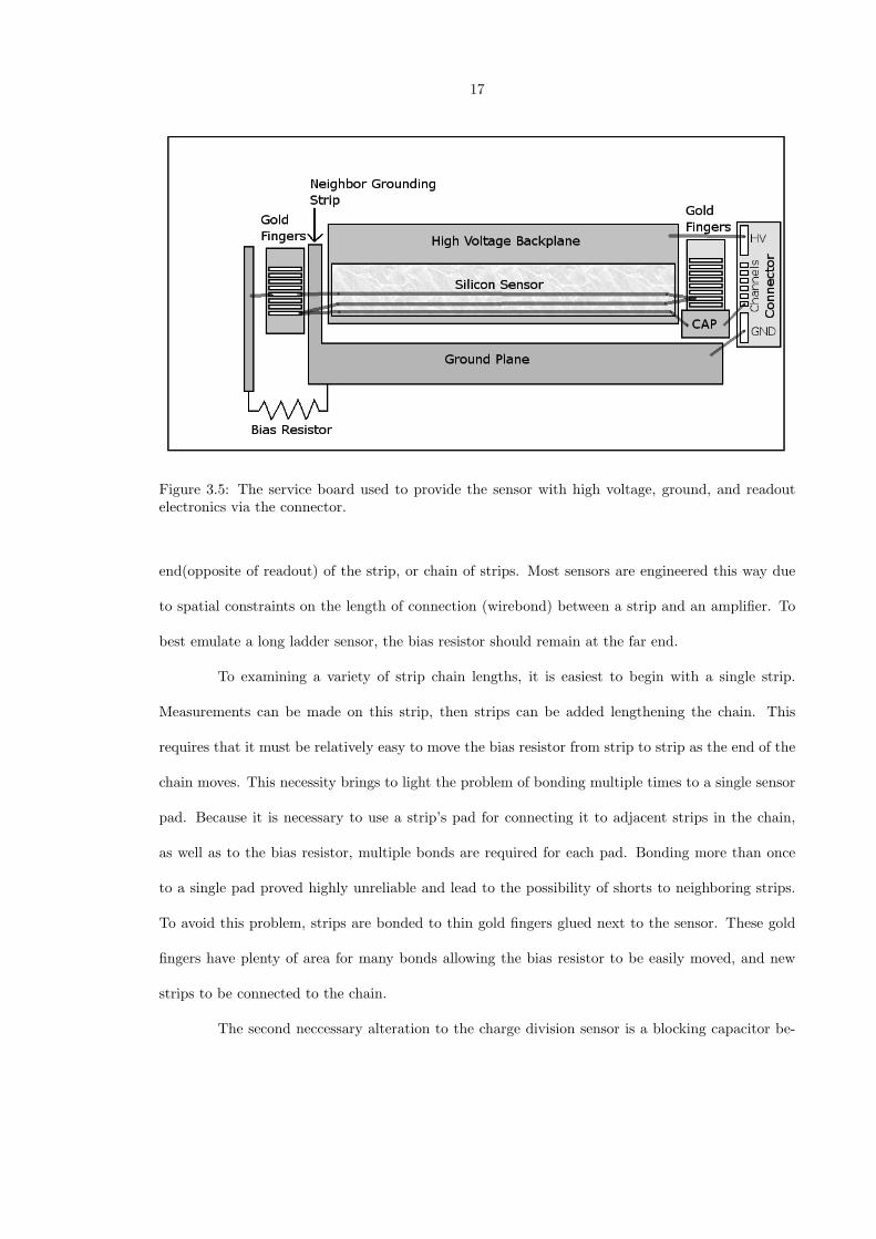
In order to have a functioning sensor, both connections to high voltage and ground are
needed, as well as a connection between strip readout pads and readout electronics. Due to the
unique requirements of the experiment, a custom service board needed to be created. The design
and manufacturing of this board proved to be one of the most difficult parts of the experiment.
Satial, electronic, and wirebonding constraints yielded the design shown in Fig. 3.5.
Pre-made connectors were available that had been designed for mating to the front-end
board. This connector provided high voltage, ground, and eight readout channels. For my purposes
only one readout channel was needed. To provide high voltage to the sensor’s backside, wirebonds
were attached from the connector to the copper side of a piece of copper-plated G10. This piece of
G10 previously had much of its copper milled off leaving just the high voltage backside plane and
the ground plane as shown in Fig. 3.5. The ground plane was established by connecting wirebonds
from the copper plane to the connector. The ground plane’s design was developed to provide ground
to neighboring strips as well as the adapted bias resistor.
As mentioned in section 3.4, the charge division sensor needed two alterations, the first
being an added bias resistor. In common AC-biased sensors each strip is connected to a bias resistor
that is connected to ground. This provides a voltage reference for each implant strip, and helps
establish the electric field desired in the sensor. Because all the strips on the charge division sensor
are floating, a bias resistor needed to be added. The desired location of this resistor is the far
17
Figure 3.5: The service board used to provide the sensor with high voltage, ground, and readoutelectronics via the connector.
end(opposite of readout) of the strip, or chain of strips. Most sensors are engineered this way due
to spatial constraints on the length of connection (wirebond) between a strip and an amplifier. To
best emulate a long ladder sensor, the bias resistor should remain at the far end.
To examining a variety of strip chain lengths, it is easiest to begin with a single strip.
Measurements can be made on this strip, then strips can be added lengthening the chain. This
requires that it must be relatively easy to move the bias resistor from strip to strip as the end of the
chain moves. This necessity brings to light the problem of bonding multiple times to a single sensor
pad. Because it is necessary to use a strip’s pad for connecting it to adjacent strips in the chain,
as well as to the bias resistor, multiple bonds are required for each pad. Bonding more than once
to a single pad proved highly unreliable and lead to the possibility of shorts to neighboring strips.
To avoid this problem, strips are bonded to thin gold fingers glued next to the sensor. These gold
fingers have plenty of area for many bonds allowing the bias resistor to be easily moved, and new
strips to be connected to the chain.
The second neccessary alteration to the charge division sensor is a blocking capacitor be-

18
tween the sensor and readout system. Because only one strip of the chain will be connected to
readout, only one capacitor is needed (as seen in Fig. 3.5 labeled ’CAP’, 1.5uF). Pieces of gold were
soldered to this capacitor so that it could be bonded to the sensor and connector. It is important
to note that because the readout connector is on one side of the service board, and the bias resistor
is on the other, only strip chains of an odd number of strips can be properly measured. Figure 3.5
shows an example chain of three strips.
The small 50um pitch (spacing between readout strips) of the charge division sensor is very
important, and led to many constraints on the service board. Because the long ladders considered in
the SID detector design will be approximately 80-100cm (17-21 strips) long, I would ideally like to
examine a chain of strips nearly that long. The constraining factor to strip chain length is the pitch
of the gold fingers used. The pitch was approximately 500um, or about ten times that of the sensor.
Because the sensor had 128 strips, this allowed for 13 strips to be connected in series. While this is
less than the length desired, the resistance of the ladders is comparable due to the high resistance
of the narrow charge division strips.
The last modification to the sensor is the grounding of neighboring strips. Neighboring
strips are those adjacent to the strips being measured in the chain. By grounding these strips, the
cross-talk noise component that may compromise results is eliminated. I measured the difference
between having neighboring strips grounded, and leaving them floating, to be very slight for sin-
gle strips. Despite the small difference, every strip added to the chain had its neighboring strips
grounded. To ground these strips a thing piece of gold was placed on the edge of the sensor on the
bias resistor side. This piece of gold was then connected to the ground plane and wirebonds were
connected from neighboring strips to the gold.
19
4 Results and Analysis
Before making estimations and measurements on the charge division sensor, it is necessary
to determine some characteristics of the amplifier. As noted in Eq. 2.5 in section 2.2, ina, ena, and Af
are constants that characterize our amplifier. It is assumed that ina is approximately zero because
RC2 terms dominate for our sensor estimations due to the large resistance and capacitance values.
The current fluctuations in the amplifier are small compared with the noise charge generated by
voltage fluctuations, ena, and large capacitances (Q = CV ). Therefore, only two unknowns are left
to be determined. Because τ and Fv do not vary significantly, ena and Af can be taken to be a
single constant, β, and solved for using known component values and measurements. Rearranging
Eq. 2.5 and dropping ina results in Eq. 4.1. It is simplest, however, to use noise measurements on
single capacitors. For a single capacitor Eq. 4.1 becomes 4.2 because Rs = 0, Rb →∞, and Id = 0.
[Q2 − Fiτ(2eId + 4kT
Rb) + FvC
2
τ 4kTRsC2
]= Fv(
1τe2na + 4Af ) = β (4.1)
[Q2
C2
]= Fv(
1τe2na + 4Af ) = β (4.2)
The relationship between Q and C can be determined by examining a plot of noise mea-
surements taken at different capacitances. Examining this plot is important because if Q and C are
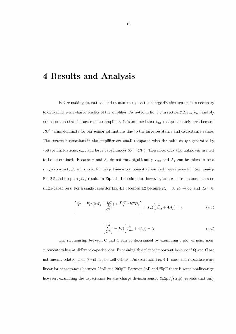
not linearly related, then β will not be well defined. As seen from Fig. 4.1, noise and capacitance are
linear for capacitances between 25pF and 200pF. Between 0pF and 25pF there is some nonlinearity;
however, examining the capacitance for the charge division sensor (5.2pF/strip), reveals that only
20
strip lengths under five will be subject to this nonlinearity. Because my primary concern is long
strip lengths I will take the slope of this graph between 25 and 200pF to be β. Fitting the data
points yields Q[e] = 393 + 9.1C[pF ], and therefore β = 9.1 epF . Rearranging Eq. 4.1 I find Eq. 4.3
below.
Figure 4.1: Noise measured for different values of capacitance using the LTSFE chip and setupdescribed in section 3.1. Shaper Current set to 300nA
Q2 = Fiτ(2eId +4kTRb
) +FvC
2
τ4kTRs + FvC
2β (4.3)
With the setup intact and understood, the first measurements needed are noise measure-
ments of individual strips on the charge division sensor. Because I cannot measure each strip
individually before adding it to the chain, an estimate of the noise variation of strips is needed.
Out of the 128 strips on the sensor, only 13 strips are used in the chain (spaced every 10 strips
with their neighbors grounded). This leaves a few strips for which it is possible to make individual
noise measurements. Spatial constraints limited this measure to only four different strips; however,
examining these strips showed that noise measurements did not vary significantly between strips
(see Table 4.1).

21
Strip # noise(e)Strip 6 469Strip 10 456Strip 15 491Strip 17 494Average 477RMS 18
Table 4.1: Noise measurements for different strips on the charge division sensor. Strip number refersto the number of the strip measured seen on the actual sensor itself.
Now that I know the variance between different strips is low, I can check to see how well
these measurements agree with predicted results. Using Eq. 4.3 estimations can be made. For one
strip on the charge division sensor with characteristics listed in Table 4.2, the estimated noise value
is 446e, which compared with the average noise measurement of strips 6, 10, 15, and 17, is only
a 1.7σ difference. This difference may be attributed to the amplifier noise term, ina, which was
neglected.
Charge Division SensorId (nA) 2.7×10⁻¹⁰
Rb (Ω) 4.40×10⁷
Rs (Ω) 287C (F ) 5.2×10⁻¹²
Table 4.2: Characteristics of the charge division sensor.
Since estimations and measurements appear to agree, more interesting noise measurements
on long ladders can be taken. Adding two more strips to the chain (only odd strip numbers can be
measured, see section 3.5) yielded a noise measurement of 569e. To make estimations for this three-
strip design, it is important to note which sensor characteristics depend on the number of strips.
The sensor’s strip resistance should add linearly yielding three times the resistance of a single strip.
The sensor’s capacitance should also add linearly because adding strips to the chain is effectively
increasing the surface area that may generate a capacitance. The current leak through the sensor
will again add linearly because adding additional strips is just like connecting sensors in series. The
bias resistor placed at the end of the sensor will not change value. Using this logic, the estimated

22
noise of a three strip chain is 580e.
By plotting measurements and estimations of each strip chain length I can see graphically
how they agree and differ. The more relevant estimations are those from our rigorous equation
that includes amplifier characteristics and shaping factors (Eq. 4.3); however, estimations from the
simplified, assumed CR-RC shaper equation (Eq. 2.6)could also be examined to show the inaccuracies
of these assumptions at long sensor lengths. Fig. 4.2 shows these estimations alongside actual
measurements taken on the charge division sensor for strip chains as long as 13 strips.
Figure 4.2: A graph of noise estimations and measurements examining each length of the strip chainon the charge division sensor.
My primary concern in this study is the large predicted effect of strip noise at long ladder
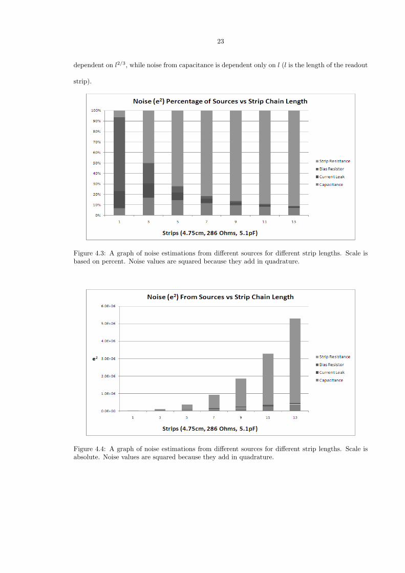
lengths. The plots displayed below examine how large this effect is relative to other noise sources.
Plots 4.3 and 4.4 show the noise generated by strip resistance, bias resistance, current leak, and
capacitance. Because noise adds in quadrature, these plots are shown in squared equivalent noise
charge. It can be seen that for a single strip length, bias resistance is the dominating factor. When
strip lengths increase, capacitance and strip resistance become the two largest terms. As strip
lengths continue to grow, strip resistance begins to dominate because noise from strip resistance is
23
dependent on l2/3, while noise from capacitance is dependent only on l (l is the length of the readout
strip).
Figure 4.3: A graph of noise estimations from different sources for different strip lengths. Scale isbased on percent. Noise values are squared because they add in quadrature.
Figure 4.4: A graph of noise estimations from different sources for different strip lengths. Scale isabsolute. Noise values are squared because they add in quadrature.
24
5 Conclusion
Figure 4.2 clearly shows a deviation from the expected measurements. Noise measurements
for strip chains longer than five strips are significantly lower than estimations. There is also a sharp
difference between rigorous and simplified estimations. This difference emphasizes the importance
of amplifier characteristics, and their strong dependence on input pulse heights.
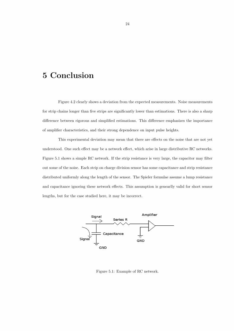
This experimental deviation may mean that there are effects on the noise that are not yet
understood. One such effect may be a network effect, which arise in large distributive RC networks.
Figure 5.1 shows a simple RC network. If the strip resistance is very large, the capacitor may filter
out some of the noise. Each strip on charge division sensor has some capacitance and strip resistance
distributed uniformly along the length of the sensor. The Spieler formulae assume a lump resistance
and capacitance ignoring these network effects. This assumption is genearlly valid for short sensor
lengths, but for the case studied here, it may be incorrect.
Figure 5.1: Example of RC network.

25
5.1 Further Studies
A simulation would be helpful to confirm these results. Creating a SPICE (Simulation
Program with Integrated Circuit Emphasis) model to estimate the noise for long ladder detector
systems would be ideal. Such model was successful for studies of ATLAS ACT sensor performance,
where the strip length was short (only 12cm), but the shaping time was ∼50 times smaller (∼25
ns),exacerbating the effect of the strip resistance noise.[5]
A question arising in the experimental design is the location of the input pulse relative
to the strip chain. Detectors used in particle accelerators are bombarded with particles at random
locations. For this experiment the input pulse was delivered via the connector and therefore always
at the readout end of the sensor. If the equivalent noise charge measured is sensitive to the input
pulse location, then this experiment is incomplete. If perhaps the signal is attenuated significantly
due to the high resistance strips, then another design that would allow the injection of charge at
different locations on the chain would be necessary. Charge division studies, conducted in SCIPP labs
by Jerome Carman1, for very high resistance strips (600kΩ), have yielded results that show a noise
dependence on charge injection location. While a location dependence study may be experimentally
challenging, if future SPICE simulations show a significant location dependence on charge injection,
this will be an important future study.
1Jerome Carman, UCSC undergraduate, SCIPP. Private communication
26
Bibliography
[1] Spieler, Helmuth. Semiconductor Detector Systems, Oxford University Press, New York, 2005.
[2] International Linear Collider Design Reference Report. Vol 4: Detectors, p20. August 2007
[3] J. Phys. G: Nucl. Part. Phys. 33 (2006) 1
[4] ROOT: An object oriented data analysis framework, Rene Brun and Fons Rademakers Linux
Journal 998July Issue 51, Metro Link Inc, (English).
[5] Kipnis I., Noise Analysis due to Strip Resistance in the ATLAS SCT Silicon Strip Module,
LBNL Note 39307, 1996.