Embed Size (px)
Citation preview
Investigation of non-equilibrium steady-stategain in semiconductor quantum wells
P.J. Bream, S. Sujecki and E.C. Larkins
Abstract: A dynamic quantum well (QW) gain model is presented, which is used to investigatenon-equilibrium steady-state gain in a QW, under CW electrical and optical excitations.Intrasubband, intersubband and interband carrier–carrier and carrier–phonon scattering processesare distinguished. Carrier capture/escape is modelled as a carrier–carrier scattering process andincludes the solution of Poisson’s equation, such that deviations from QW charge neutrality leadto a modification of the capture rate through band bending. Radiative transitions are modelledusing a Fermi’s Golden Rule approach. Carrier–carrier scattering is described using the standardrelaxation rate approximation. A different approach is adopted for carrier–phonon interactions toaccount for the carrier kinetic energy thresholds, which exist for intrasubband and intersubbandcarrier–phonon scattering by phonon emission and absorption. Results show that significantnon-equilibrium conditions exist, even in the absence of stimulated emission, and have impli-cations for the use of thermal equilibrium carrier distributions in full laser diode simulation tools.
1 Introduction
Common commercial applications of quantum well (QW)semiconductor laser diodes rely on the linearity of theiroperating characteristics. However, nonlinear opticalphenomena begin to manifest themselves at high operatingpowers and speeds [1, 2]. These are, of course, detrimentalto many applications, such as high peak power pulsed IRlaser sources, which, when frequency-doubled, result inhigh-quality sources for medicine [3]. At the same time,however, the exploitation of these optical nonlinearities pro-vides interesting possibilities for the design of functionalphotonic devices [4–6], such as all-optical switches andwavelength converters.
The three main processes, spectral hole burning (SHB)[7], carrier heating (CH) [8] and carrier density pulsations[9], which give rise to optical nonlinearities, tend to occuron ultrafast timescales, ranging from a few nanosecondsto hundreds of femtoseconds [10]. The manifestation of non-linear behaviour, such as gain saturation [11] or spatial holeburning [12], can be measured experimentally [13, 14].However, the details of the non-equilibrium carrierdistributions, which are responsible for the nonlinearity,cannot generally be observed directly, even usingpump-probe [15] and time-resolved photoluminescence[16] experiments. To achieve a detailed understanding ofthese ultrafast nonlinear processes, theoretical models arerequired. All of the characteristics of the QW material,such as band structure, gain and carrier relaxation processes,must be described correctly to create a model with sufficientaccuracy to be predictive. Such a model can then be used, inconjunction with experimental measurements, to investigate
# The Institution of Engineering and Technology 2006
IEE Proceedings online no. 20060038
doi:10.1049/ip-opt:20060038
Paper first received 21st April and in revised form 17th July 2006
The authors are with The University of Nottingham, University Park,Nottingham NG7 2RD, UK
E-mail: [email protected]
IEE Proc.-Optoelectron., Vol. 153, No. 6, December 2006
and characterise QW device behaviour under nonlinearoperating conditions.
Steady-state models [17–19] are of limited use for thepurpose of investigating the details of the processesgiving rise to optical nonlinearities, since they are generallybased on quasi-equilibrium formulations, which do notaccount for the ultrafast carrier scattering and relaxationprocesses involved in the generation of nonlinear opticalphenomena. Thus, time-resolved dynamic models [20, 21]are required, which include relaxation and scattering pro-cesses in detail.
Early attempts to investigate nonlinear interactions inlaser diode models relied upon simple unipolar represen-tations of the gain material and a purely phenomenologicaltreatment of the nonlinear optical susceptibility [22].Bipolar representations of the gain material were introducedusing density matrix theory, but ignored the details of thesubband dispersion and relied heavily upon the use of therelaxation rate approximation [23, 24]. In an effort torealise predictive laser models, microscopic approacheshave been developed to represent the scattering processes[25, 26]. Unfortunately, these microscopic models are com-putationally intensive and require high-performance com-puting platforms to run. Models also exist, which occupythe middle ground between detailed microscopic and sim-plistic calculations [27], but some ignore the separate QWsubbands [28].
In this paper, we describe the implementation of adynamic QW gain model, which runs on a desktop PC.The model distinguishes between intra- and intersubbandscattering processes. Carrier–carrier scattering andcarrier–phonon scattering are treated in a differentmanner. The latter uses phonon emission/absorption scat-tering to account for the carrier kinetic energy thresholdsfor intrasubband and intersubband scattering by LOphonon emission and absorption. This is expected to influ-ence non-equilibrium SHB and CH effects.
We first describe the dynamic QW gain model andpresent expressions used to describe each process in theQW. We then present results obtained for a QW under
299
CW electrical and optical excitations and discuss the impli-cations of these results for the inclusion of non-equilibriumgain in full laser diode simulation tools.
2 Model
The dynamic QW gain model calculates the temporal redis-tribution of carriers in the QW, both between subbands andwith respect to their energy. The model calculates the spec-tral properties of the QW and results may be used to includenon-equilibrium gain in a spatially resolved laser model.Equation (1) summarises the different processes contribut-ing to carrier redistributions in a particular subband, j,where the subscripts c–c and c–p are used to indicatecarrier–carrier and carrier–phonon scattering processes,intra and inter represent intrasubband and intersubbandscattering, respectively, and e-h is the electron–holeenergy relaxation process. The subscripts rad and nonradrepresent the contributions from radiative and non-radiativeinterband transitions, respectively, and cap/esc is the carriercapture and escape process into and out of the QW, respect-ively. Note that free carrier absorption (FCA) is not cur-rently included in this model. Previous studies [27] haveshown that its contribution to the nonlinear gain is smallcompared with that of SHB and, in particular, CH. Forstudies of long-wavelength structures, FCA should beincluded, since it plays a more important role [29]. Theabove processes are discussed further later in the Paper.
dnjðEÞ
dt¼
dnjðEÞ
dt
����c–c;intra
þdnjðEÞ
dt
����c–c;inter
þdnjðEÞ
dt
����e–h
þdnjðEÞ
dt
����c–p;intra
þdnjðEÞ
dt
����c–p;inter
þdnjðEÞ
dt
����rad
þdnjðEÞ
dt
����nonrad
þdnjðEÞ
dt
����cap=esc
ð1Þ
2.1 Band structure
Before the dynamic processes can be calculated, details ofthe QW band structure are required. The conduction band(CB) is assumed to be parabolic and spherically symmetric,and the valence band (VB) dispersion is calculated, alongthe k100l and k110l crystal directions, using the decoupled4-band k � p method [29]. For the results presented here,we use the standard average band-mixing coupling coeffi-cient and obtain circularly symmetric valence subbands,neglecting VB anisotropy [29, 30], for simplicity.
The time-resolved description of the QW subband carrierdistributions is a 4-dimensional (4D) problem: the carrierenergy, Ecarrier, its wavevectors, kx, ky and time, t. Toreduce the complexity of this problem and improve compu-tational efficiency, the subband isoenergy contours are inte-grated over k-space to obtain a description of the subbandcarrier distributions, which depends only on Ecarrier and t[30]. Thus, the density of states in the jth subband is simpli-fied from r(Ecarrier, kx, ky) to r(Ecarrier). In a similar manner,the optical densities of state and overlap integrals requiredfor the calculation of radiative transitions between a givenconduction and valence subband pair are also simplifiedto remove their k-dependencies, but they still retain adependence on the electron and hole energies as well asthe photon energy [30]. The description of the QW bandstructure in terms of energy rather than k leads to themain assumption of this work: all states at a given energyin a particular subband have the same occupationalprobability. This may be justified by the ultrafast
300
momentum-relaxation processes (e.g. carrier–carrier scat-tering), which occur in the QW. The relaxation lifetimesin Table 1 describe the energy relaxation rates, which areslower than the actual carrier–carrier scattering rates.Note that most models only consider circularly symmetricVB structure, even where 8- or 10-band k . p methodshave been used to calculate the VB energy dispersion[31]. This results in a one-to-one relationship between jkjand E in a particular valence subband. Thus, a circularlysymmetric VB structure implicitly assumes that all statesin a particular subband with a given value of jkj have thesame occupational probability. Other problems with the cir-cularly symmetric VB structure are that changes in thesubband and reduced densities of states caused by VB ani-sotropy are not accounted for. Furthermore, the anisotropycauses broadening of the holes burnt in the carrier energydistributions. A d-function hole burnt in the carrier energydistributions will clearly relax differently to one withfinite width and depth. Note also that in order to highlightthe details of the dynamic process, no spectral broadeninghas been included for any of the processes in the followingdiscussion [29]. Nevertheless, spectral broadening of thecarrier distributions must be considered for comparisonswith experimental data.
2.2 Carrier–carrier scattering
Carrier–carrier scattering is generally the fastest processoccurring in the QW [10], with hole–hole scatteringbeing significantly faster than electron–electron scatteringbecause of the larger hole effective mass [31]. Thisprocess is modelled using the relaxation rate approximation,as described by (2), for the intrasubband scattering process,where dnj(E)/dt is the rate of change in the number of car-riers (cm23 s21) in subband j at energy, E, rj is the associ-ated energy density of states and Pj is the carrieroccupational probability distribution. fj is a target Fermi–Dirac distribution with quasi-Fermi level Fj and
Table 1: Simulation parameters
Parameter Value
Electrons Holes
Intra- and intersubband
carrier–carrier scattering
lifetime, tc–c
0.6 ps 0.1 ps
Electron–hole scattering
lifetime, te – h
1 ps
Intra- and intersubband
carrier–LO phonon
scattering lifetime, tc–ph
1 ps 0.5 ps
LO phonon energy, hvLO 35 meV
Intra- and intersubband
carrier–acoustic phonon
scattering lifetime, tc–P
1 ns 0.5 ns
Acoustic phonon energy, hvP 0.7 meV
Carrier capture lifetime, tcap 5 ps 3 ps
SRH recombination lifetime,
tSRH
15 ns 15 ns
SRH trap energy, ET 0.6 eV below CB band edge
Auger recombination
coefficient, C
10230 cm26 s21 10230 cm26 s21
IEE Proc.-Optoelectron., Vol. 153, No. 6, December 2006
temperature Tj. tj is the associated scattering lifetime.
dnjðEÞ
dt
����c�c;intra
¼ rjðEÞPjðEÞ � fjðE;Fj; TjÞ
tj
ð2Þ
Three carrier–carrier scattering processes are included inthis model: intrasubband electron–electron (hole–hole),intersubband electron–electron (hole–hole) and interbandelectron–hole processes. Inclusion of the electron–holeprocess allows the CB electron distributions to exchangeenergy with the VB hole populations, which has beensuggested as an efficient cooling path for electrons,because of the fast hole relaxation rate [31]. The values ofFj and Tj are chosen to conserve subband carrier populationsand total energy, and depend on which of the above pro-cesses is being described. For example, for intrasubbandscattering, Pj and fj must describe carrier distributionswith the same number of carriers and the same averagecarrier energy. For electron–hole scattering, there existstwo versions of (2), one for each of the CB and VB sub-bands. The target Fermi–Dirac functions conserve thenumber of carriers in each subband and the total energyof the carriers in both subbands (i.e. they share a commontemperature but have different quasi-Fermi levels [32]).
A microscopically calculated value for the scattering life-time can be introduced in (2) and can vary between sub-bands and between processes (e.g. intrasubband orintersubband). Reported lifetimes have also been shown tovary with carrier energy [31, 33]. However, if there is aneed to use an energy-dependent tj, this indicates that therelaxation rate approximation to a Fermi–Dirac distributioncannot be used, since this would lead to a violation in theconservation of carriers and total carrier energy. In otherwords, the relaxation rate approximation cannot be usedin conjunction with an energy-dependent tj.
2.3 Carrier–phonon scattering
Carrier–phonon scattering is modelled using a model forthe emission and absorption of phonons, in a manner analo-gous to that used to model optical transitions [34]. In orderto maintain computational efficiency, energy conservationhas been maintained, but k-conservation has not, since thesimulation has been reduced to a 1D function of energy,rather than a 2D function of k. This has been achieved bymaking the assumptions that all LO (acoustic) phononshave the same energy and that the scattering probabilitybetween any two states separated by the LO phononenergy is the same. This process is described by (3),
where j ¼ l for the intrasubband process. dnj,l/dt is the
rate of change in the number of carriers (cm23 s21), Sjl is
the carrier–phonon scattering rate and rjl,eff is the effectivedensity of states for transitions between carriers with energyE1 and E2 in subband j and l. Pj,l are the carrier occupationalprobabilities and Pphon is the modal occupational prob-ability at the phonon energy, hvphon.
dnjðE1Þ
dt
����c�p
¼ �dnlðE2Þ
dt
����c�p
¼ SjlðhvphonÞrjl;eff ðE1;E2Þ�
PjðE2Þ 1� PlðE1Þ� �
þ PphonðhvphonÞ PjðE2Þ � PlðE1Þ
h in o
ð3Þ
This approach models intrasubband phonon scattering pro-cesses at the subband extrema more rigorously than the
IEE Proc.-Optoelectron., Vol. 153, No. 6, December 2006
relaxation rate approximation: carriers less than one LOphonon energy, hvLO, away from the band minimumcannot emit an LO phonon and therefore cannot contributeto the relaxation of carriers lower in energy. Equally, inter-subband carrier–phonon scattering can only occur where theenergy states in the lower subband are no more than �vLO
lower than the energy minimum of the upper subband.Finally, scattering around large peaks or holes in thecarrier distributions, which occur through strong opticalabsorption or emission, is also treated more rigorously:only carriers whose energies are hvLO away from such apeak or hole can contribute to its relaxation by carrier–LO phonon scattering. This results in phonon replicas ofthe peak or hole, which have been shown to exist throughdetailed microscopic calculations of carrier–phononinteractions [33]. Note that, we assume that the phononpopulation is in thermal equilibrium with the lattice.
2.4 Radiative recombination
Radiative transitions are described by the standard expressionresulting from Fermi’s Golden Rule [29], where bandgaprenormalisation and spectral broadening caused by manybody effects have been neglected to highlight the details ofthe dynamic processes in the QW. The expression for gainis converted into a perturbation of the carrier energy distri-butions in the standard manner [29], as shown in (4) forsubband j, where dnj/dt is the rate of change in the numberof carriers (cm23 s21); S is the density of photons withenergy hv; G, n and c are the optical confinement factor,effective index and speed of light, respectively; G (cm21) isthe gain arising from interband transitions involving carriersin subband j with energy E.
dnjðEÞ
dt
����rad
¼Xhv
GðhvÞc
nðhvÞGðE; hvÞSðhvÞ ð4Þ
2.5 Non-radiative recombination
The Shockley–Read–Hall (SRH) and Auger recombinationrates (cm23 s21) are described by the standard phenomeno-logical expressions [35], with the additional assumption thatthe excited electron or hole resulting from the Augerprocess escapes from the QW. This is a reasonable assump-tion for the materials we are studying, since a carrier excitedto an energy .1.2 eV away from the band minimum ismuch more likely to scatter into the material surroundingthe QW than relax back to a confined state. Non-radiativerecombination is then assumed to be distributed across theQW energy states according to their level of occupation,as described by (5) for subband j, where Rnonrad is thetotal non-radiative recombination rate and Ntot is the totalcarrier population in the CB or VB.
dnjðEÞ
dt
����nonrad
¼ Rnonrad
njðEÞ
Ntot
ð5Þ
2.6 Carrier capture/escape
Carrier capture/escape between the QW and barrier regionsis modelled as a 3D$ 2D$ 3D carrier–carrier scatteringprocess, as described by (6) for subband j. The 3D barrierpopulations are described by Fermi–Dirac distributions,
301
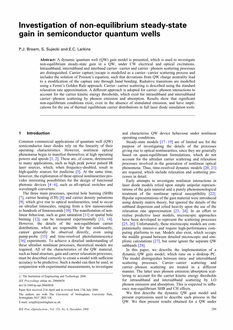
Fig. 1 Different CW electrical excitation levels
a CB electron energy distributionb VB hole energy distribution
f3D, in thermal equilibrium with the lattice.
dnjðEÞ
dt
����cap=esc
¼ rjðEÞf3DðEÞ � PjðEÞ
tcap=esc
ð6Þ
In (11), tcap/esc is the capture/escape rate and, as for thecarrier–carrier relaxation processes, is faster for holesthan electrons. Thus, high-energy carriers from the barriersare injected into the top of the QW and relax down into theQW through phonon emission. This is the main mechanismfor CH under steady-state injection in the absence of stimu-lated emission.
In addition, Poisson’s equation is solved for the region sur-rounding the QW, such that deviations from QW chargeneutrality caused by the different electron and hole capture/escape and relaxation rates result in band bending. This actsas a negative feedback mechanism to drive the net electronand hole capture rates towards the same value, since thesemust be equal at steady state. This also prevents chargeaccumulating in the QW without limit. Both of these arereal mechanisms in real devices. The result of this treatmentis a variation of the barrier region carrier distributions as afunction of QW charge neutrality. Thus, although an initial3D barrier electron and hole density (N3D, P3D) determines
302
electrical excitation of the QW in this model, these valuesmay change according to the QW electron and hole popu-lations. Note that, because the dynamic QW gain modeldoes not self-consistently solve the Schrodinger and Poissonequations, the excess charge in the QW is assumed to beuniformly distributed across the QW.
3 Results
Using the model described earlier, we have investigated theresponse of a�9 nm InGaAs/InGaAsP QW to CW electricaland optical excitations. The excitation levels were defined byN3D ¼ P3D, in the range 1015 to 2 � 1017 cm23, and thephoton density, S, at an energy of 1.249 eV, in the range 0to 1016 cm23, respectively. Note, for example, that a photondensity of 1015 cm23 corresponds to �2 mW of opticalpower incident on a 3 mm-wide ridge waveguide amplifier.
Published scattering parameters for all of the aforemen-tioned processes vary significantly, even for a given QW.Thus, parameters were chosen from a number of sources[10, 31, 36] to estimate the correct order of magnitude ofeach of the relaxation processes, such that an idea of the rela-tive importance of each process can been shown. The par-ameters used for the calculations in this work are shown inTable 1.
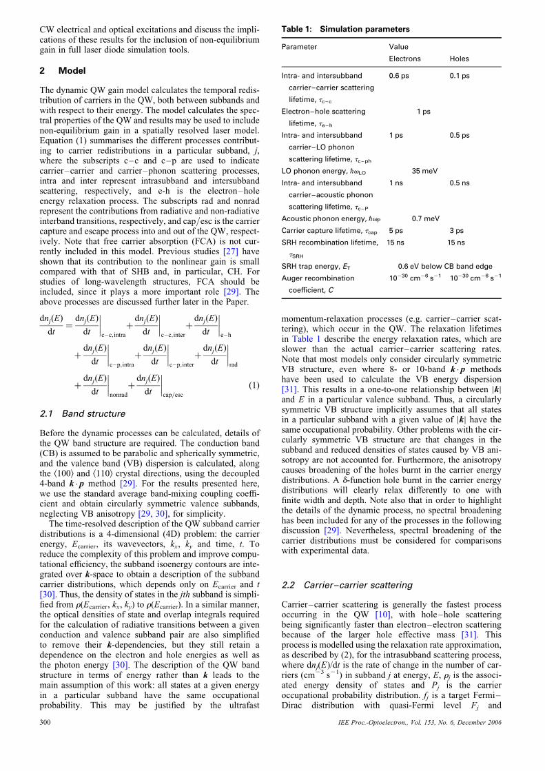
Fig. 2 Different CW optical excitation levels and N3D ¼ P3D ¼ 1017 cm23
a CB electron energy distributionb VB hole energy distribution
IEE Proc.-Optoelectron., Vol. 153, No. 6, December 2006
Figs. 1a and b show the steady-state QW electron and holeenergy distributions, respectively, for various levels of elec-trical excitation. Note that a significant population of con-fined carriers exists above the QW (Ee . Vc, jEhj . jVvj).Figs. 2a and b show the electron and hole energy distri-butions, respectively, for various photon densities andN3D ¼ P3D ¼ 1017 cm23. A higher rate of stimulated emis-sion depletes the QW populations and also results in SHB,
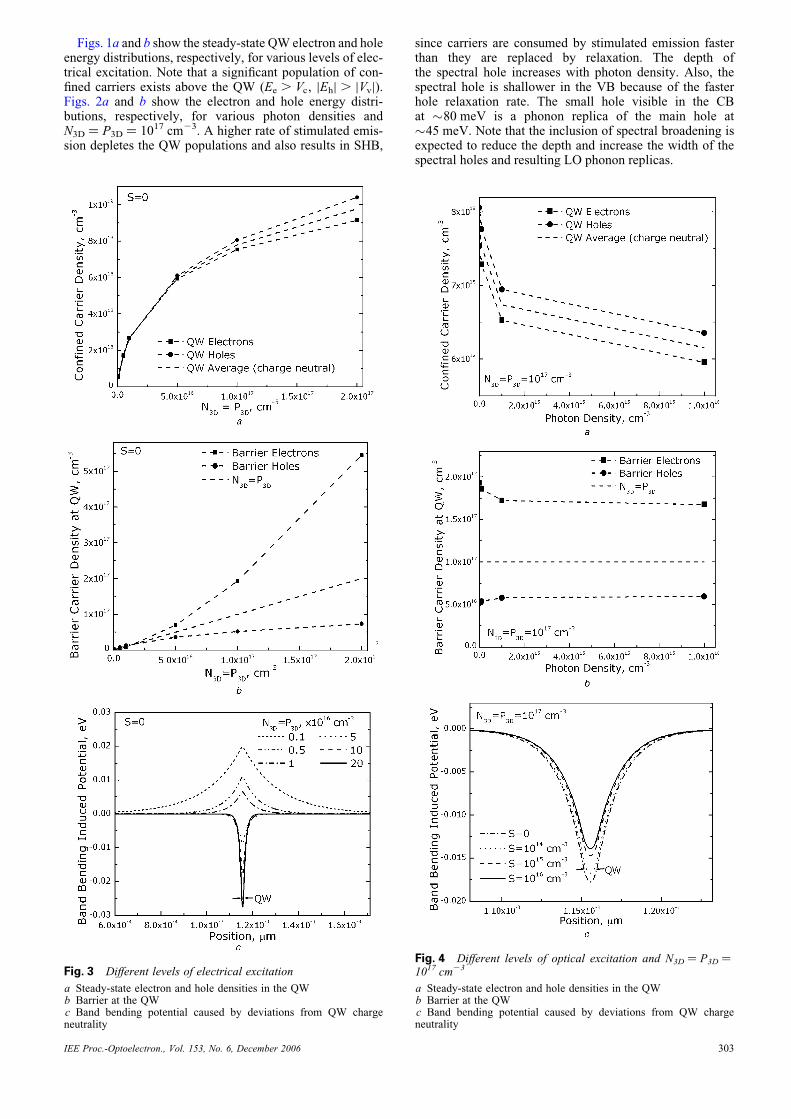
Fig. 3 Different levels of electrical excitation
a Steady-state electron and hole densities in the QWb Barrier at the QWc Band bending potential caused by deviations from QW chargeneutrality
IEE Proc.-Optoelectron., Vol. 153, No. 6, December 2006
since carriers are consumed by stimulated emission fasterthan they are replaced by relaxation. The depth ofthe spectral hole increases with photon density. Also, thespectral hole is shallower in the VB because of the fasterhole relaxation rate. The small hole visible in the CBat �80 meV is a phonon replica of the main hole at�45 meV. Note that the inclusion of spectral broadening isexpected to reduce the depth and increase the width of thespectral holes and resulting LO phonon replicas.
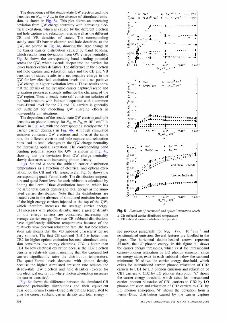
Fig. 4 Different levels of optical excitation and N3D ¼ P3D ¼1017 cm23
a Steady-state electron and hole densities in the QWb Barrier at the QWc Band bending potential caused by deviations from QW chargeneutrality
303
The dependence of the steady-state QW electron and holedensities on N3D ¼ P3D, in the absence of stimulated emis-sion, is shown in Fig. 3a. This plot shows an increasingdeviation from QW charge neutrality with increasing elec-trical excitation, which is caused by the different electronand hole capture and relaxation rates as well as the differentCB and VB densities of states. The correspondingsteady-state 3D barrier electron and hole densities, at theQW, are plotted in Fig. 3b, showing the large change inthe barrier carrier distribution caused by band bending,which results from deviations from QW charge neutrality.Fig. 3c shows the corresponding band bending potentialacross the QW, which extends deeper into the barriers forlower barrier carrier densities. The difference in the electronand hole capture and relaxation rates and the CB and VBdensities of states results in a net negative charge in theQW for low electrical excitation levels and a net positiveQW charge at higher excitation levels. These results showthat the details of the dynamic carrier capture/escape andrelaxation processes strongly influence the charging of theQW region. Thus, a steady-state self-consistent solution ofthe band structure with Poisson’s equation with a commonquasi-Fermi level for the 2D and 3D carriers is generallynot sufficient for modelling QW charging effects innon-equilibrium situations.
The dependence of the steady-state QW electron and holedensities on photon density, for N3D ¼ P3D ¼ 1017 cm23 isshown in Fig. 4a, with the corresponding steady-state 3Dbarrier carrier densities in Fig. 4b. Although stimulatedemission consumes QW electrons and holes at the samerate, the different electron and hole capture and relaxationrates lead to small changes in the QW charge neutralityfor increasing optical excitation. The corresponding bandbending potential across the QW is shown in Fig. 4c,showing that the deviation from QW charge neutralityslowly decreases with increasing photon density.
Figs. 5a and b show the subband carrier distributiontemperatures as a function of electrical and optical exci-tation, for the CB and VB, respectively. Fig. 5c shows thecorresponding quasi-Fermi levels. The distribution tempera-ture and quasi-Fermi level for each subband is calculated byfinding the Fermi–Dirac distribution function, which hasthe same total carrier density and total energy as the simu-lated carrier distribution. Note that the distributions areheated even in the absence of stimulated emission becauseof the high-energy carriers injected at the top of the QW,which therefore increases the average carrier energy.CH increases with photon density, since a greater densityof low energy carriers are consumed, increasing theaverage carrier energy. The two CB subband distributionshave significantly different temperatures because of therelatively slow electron relaxation rate (the fast hole relax-ation rate means that the VB subband characteristics arevery similar). The first CB subband (CB1) is hotter thanCB2 for higher optical excitation because stimulated emis-sion consumes low energy electrons. CB2 is hotter thanCB1 for low electrical excitation because the CB2 electrondensity is relatively small, meaning that the captured hotcarriers significantly raise the distribution temperature.The quasi-Fermi levels decrease with photon densitybecause the higher stimulated emission rate reduces thesteady-state QW electron and hole densities (except forlow electrical excitation, where photon absorption increasesthe carrier densities).
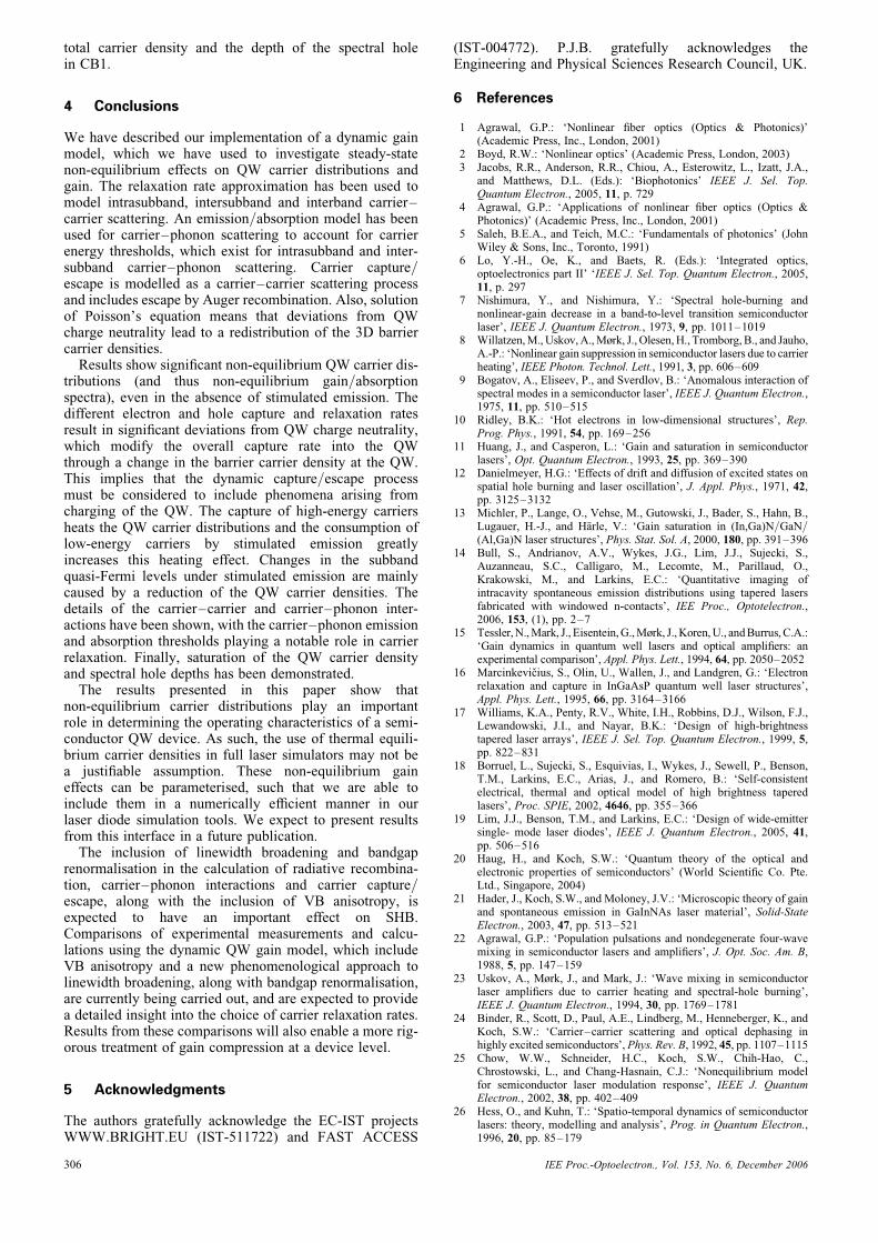
Fig. 6a shows the difference between the simulated CBsubband probability distributions and their equivalentquasi-equilibrium Fermi–Dirac distributions (calculated togive the correct subband carrier density and total energy –
304
see previous paragraph) for N3D ¼ P3D ¼ 1017 cm23 andno stimulated emission. Several features are labelled in thefigure. The horizontal double-headed arrows represent35 meV, the LO phonon energy. In this figure ‘a’ showsthe carrier energy thresholds, which exist for intrasubbandcarrier–phonon relaxation by LO phonon emission, sinceno energy states exist in each subband below the subbandminimum; ‘b’ shows the carrier energy threshold, whichexists for intersubband carrier–phonon relaxation of CB2carriers to CB1 by LO phonon emission and relaxation ofCB1 carriers to CB2 by LO phonon absorption; ‘c’ showsthe carrier energy threshold, which exists for intersubbandcarrier–phonon relaxation of CB1 carriers to CB2 by LOphonon emission and relaxation of CB2 carriers to CB1 byLO phonon absorption; ‘d’ shows the deviation from aFermi–Dirac distribution caused by the carrier capture
Fig. 5 Function of electrical and optical excitation levels
a CB subband carrier distributed temperatureb VB subband carrier distributed temperature
IEE Proc.-Optoelectron., Vol. 153, No. 6, December 2006
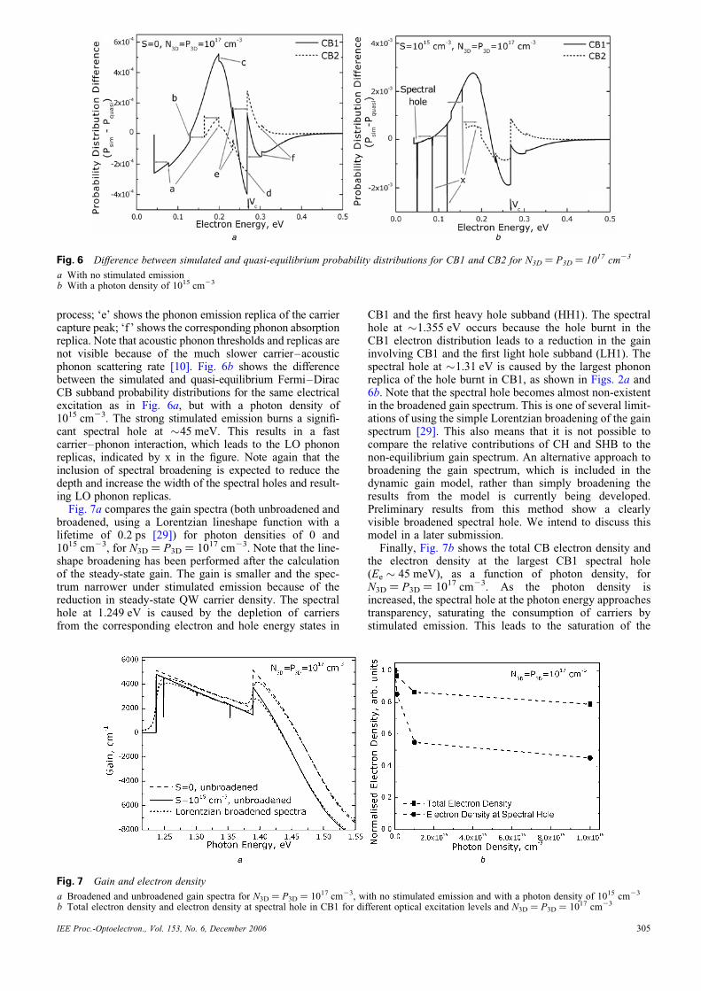
Fig. 6 Difference between simulated and quasi-equilibrium probability distributions for CB1 and CB2 for N3D ¼ P3D ¼ 1017 cm23
a With no stimulated emissionb With a photon density of 1015 cm23
process; ‘e’ shows the phonon emission replica of the carriercapture peak; ‘f ’ shows the corresponding phonon absorptionreplica. Note that acoustic phonon thresholds and replicas arenot visible because of the much slower carrier–acousticphonon scattering rate [10]. Fig. 6b shows the differencebetween the simulated and quasi-equilibrium Fermi–DiracCB subband probability distributions for the same electricalexcitation as in Fig. 6a, but with a photon density of1015 cm23. The strong stimulated emission burns a signifi-cant spectral hole at �45 meV. This results in a fastcarrier–phonon interaction, which leads to the LO phononreplicas, indicated by x in the figure. Note again that theinclusion of spectral broadening is expected to reduce thedepth and increase the width of the spectral holes and result-ing LO phonon replicas.
Fig. 7a compares the gain spectra (both unbroadened andbroadened, using a Lorentzian lineshape function with alifetime of 0.2 ps [29]) for photon densities of 0 and1015 cm23, for N3D ¼ P3D ¼ 1017 cm23. Note that the line-shape broadening has been performed after the calculationof the steady-state gain. The gain is smaller and the spec-trum narrower under stimulated emission because of thereduction in steady-state QW carrier density. The spectralhole at 1.249 eV is caused by the depletion of carriersfrom the corresponding electron and hole energy states in
IEE Proc.-Optoelectron., Vol. 153, No. 6, December 2006
CB1 and the first heavy hole subband (HH1). The spectralhole at �1.355 eV occurs because the hole burnt in theCB1 electron distribution leads to a reduction in the gaininvolving CB1 and the first light hole subband (LH1). Thespectral hole at �1.31 eV is caused by the largest phononreplica of the hole burnt in CB1, as shown in Figs. 2a and6b. Note that the spectral hole becomes almost non-existentin the broadened gain spectrum. This is one of several limit-ations of using the simple Lorentzian broadening of the gainspectrum [29]. This also means that it is not possible tocompare the relative contributions of CH and SHB to thenon-equilibrium gain spectrum. An alternative approach tobroadening the gain spectrum, which is included in thedynamic gain model, rather than simply broadening theresults from the model is currently being developed.Preliminary results from this method show a clearlyvisible broadened spectral hole. We intend to discuss thismodel in a later submission.
Finally, Fig. 7b shows the total CB electron density andthe electron density at the largest CB1 spectral hole(Ee � 45 meV), as a function of photon density, forN3D ¼ P3D ¼ 1017 cm23. As the photon density isincreased, the spectral hole at the photon energy approachestransparency, saturating the consumption of carriers bystimulated emission. This leads to the saturation of the
Fig. 7 Gain and electron density
a Broadened and unbroadened gain spectra for N3D ¼ P3D ¼ 1017 cm23, with no stimulated emission and with a photon density of 1015 cm23
b Total electron density and electron density at spectral hole in CB1 for different optical excitation levels and N3D ¼ P3D ¼ 1017 cm23
305
total carrier density and the depth of the spectral holein CB1.
4 Conclusions
We have described our implementation of a dynamic gainmodel, which we have used to investigate steady-statenon-equilibrium effects on QW carrier distributions andgain. The relaxation rate approximation has been used tomodel intrasubband, intersubband and interband carrier–carrier scattering. An emission/absorption model has beenused for carrier–phonon scattering to account for carrierenergy thresholds, which exist for intrasubband and inter-subband carrier–phonon scattering. Carrier capture/escape is modelled as a carrier–carrier scattering processand includes escape by Auger recombination. Also, solutionof Poisson’s equation means that deviations from QWcharge neutrality lead to a redistribution of the 3D barriercarrier densities.
Results show significant non-equilibrium QW carrier dis-tributions (and thus non-equilibrium gain/absorptionspectra), even in the absence of stimulated emission. Thedifferent electron and hole capture and relaxation ratesresult in significant deviations from QW charge neutrality,which modify the overall capture rate into the QWthrough a change in the barrier carrier density at the QW.This implies that the dynamic capture/escape processmust be considered to include phenomena arising fromcharging of the QW. The capture of high-energy carriersheats the QW carrier distributions and the consumption oflow-energy carriers by stimulated emission greatlyincreases this heating effect. Changes in the subbandquasi-Fermi levels under stimulated emission are mainlycaused by a reduction of the QW carrier densities. Thedetails of the carrier–carrier and carrier–phonon inter-actions have been shown, with the carrier–phonon emissionand absorption thresholds playing a notable role in carrierrelaxation. Finally, saturation of the QW carrier densityand spectral hole depths has been demonstrated.
The results presented in this paper show thatnon-equilibrium carrier distributions play an importantrole in determining the operating characteristics of a semi-conductor QW device. As such, the use of thermal equili-brium carrier densities in full laser simulators may not bea justifiable assumption. These non-equilibrium gaineffects can be parameterised, such that we are able toinclude them in a numerically efficient manner in ourlaser diode simulation tools. We expect to present resultsfrom this interface in a future publication.
The inclusion of linewidth broadening and bandgaprenormalisation in the calculation of radiative recombina-tion, carrier–phonon interactions and carrier capture/escape, along with the inclusion of VB anisotropy, isexpected to have an important effect on SHB.Comparisons of experimental measurements and calcu-lations using the dynamic QW gain model, which includeVB anisotropy and a new phenomenological approach tolinewidth broadening, along with bandgap renormalisation,are currently being carried out, and are expected to providea detailed insight into the choice of carrier relaxation rates.Results from these comparisons will also enable a more rig-orous treatment of gain compression at a device level.
5 Acknowledgments
The authors gratefully acknowledge the EC-IST projectsWWW.BRIGHT.EU (IST-511722) and FAST ACCESS
306
(IST-004772). P.J.B. gratefully acknowledges theEngineering and Physical Sciences Research Council, UK.
6 References
1 Agrawal, G.P.: ‘Nonlinear fiber optics (Optics & Photonics)’(Academic Press, Inc., London, 2001)
2 Boyd, R.W.: ‘Nonlinear optics’ (Academic Press, London, 2003)3 Jacobs, R.R., Anderson, R.R., Chiou, A., Esterowitz, L., Izatt, J.A.,
and Matthews, D.L. (Eds.): ‘Biophotonics’ IEEE J. Sel. Top.Quantum Electron., 2005, 11, p. 729
4 Agrawal, G.P.: ‘Applications of nonlinear fiber optics (Optics &Photonics)’ (Academic Press, Inc., London, 2001)
5 Saleh, B.E.A., and Teich, M.C.: ‘Fundamentals of photonics’ (JohnWiley & Sons, Inc., Toronto, 1991)
6 Lo, Y.-H., Oe, K., and Baets, R. (Eds.): ‘Integrated optics,optoelectronics part II’ ‘IEEE J. Sel. Top. Quantum Electron., 2005,11, p. 297
7 Nishimura, Y., and Nishimura, Y.: ‘Spectral hole-burning andnonlinear-gain decrease in a band-to-level transition semiconductorlaser’, IEEE J. Quantum Electron., 1973, 9, pp. 1011–1019
8 Willatzen, M., Uskov, A., Mørk, J., Olesen, H., Tromborg, B., and Jauho,A.-P.: ‘Nonlinear gain suppression in semiconductor lasers due to carrierheating’, IEEE Photon. Technol. Lett., 1991, 3, pp. 606–609
9 Bogatov, A., Eliseev, P., and Sverdlov, B.: ‘Anomalous interaction ofspectral modes in a semiconductor laser’, IEEE J. Quantum Electron.,1975, 11, pp. 510–515
10 Ridley, B.K.: ‘Hot electrons in low-dimensional structures’, Rep.Prog. Phys., 1991, 54, pp. 169–256
11 Huang, J., and Casperon, L.: ‘Gain and saturation in semiconductorlasers’, Opt. Quantum Electron., 1993, 25, pp. 369–390
12 Danielmeyer, H.G.: ‘Effects of drift and diffusion of excited states onspatial hole burning and laser oscillation’, J. Appl. Phys., 1971, 42,pp. 3125–3132
13 Michler, P., Lange, O., Vehse, M., Gutowski, J., Bader, S., Hahn, B.,Lugauer, H.-J., and Harle, V.: ‘Gain saturation in (In,Ga)N/GaN/(Al,Ga)N laser structures’, Phys. Stat. Sol. A, 2000, 180, pp. 391–396
14 Bull, S., Andrianov, A.V., Wykes, J.G., Lim, J.J., Sujecki, S.,Auzanneau, S.C., Calligaro, M., Lecomte, M., Parillaud, O.,Krakowski, M., and Larkins, E.C.: ‘Quantitative imaging ofintracavity spontaneous emission distributions using tapered lasersfabricated with windowed n-contacts’, IEE Proc., Optotelectron.,2006, 153, (1), pp. 2–7
15 Tessler, N., Mark, J., Eisentein, G., Mørk, J., Koren, U., and Burrus, C.A.:‘Gain dynamics in quantum well lasers and optical amplifiers: anexperimental comparison’, Appl. Phys. Lett., 1994, 64, pp. 2050–2052
16 Marcinkevicius, S., Olin, U., Wallen, J., and Landgren, G.: ‘Electronrelaxation and capture in InGaAsP quantum well laser structures’,Appl. Phys. Lett., 1995, 66, pp. 3164–3166
17 Williams, K.A., Penty, R.V., White, I.H., Robbins, D.J., Wilson, F.J.,Lewandowski, J.I., and Nayar, B.K.: ‘Design of high-brightnesstapered laser arrays’, IEEE J. Sel. Top. Quantum Electron., 1999, 5,pp. 822–831
18 Borruel, L., Sujecki, S., Esquivias, I., Wykes, J., Sewell, P., Benson,T.M., Larkins, E.C., Arias, J., and Romero, B.: ‘Self-consistentelectrical, thermal and optical model of high brightness taperedlasers’, Proc. SPIE, 2002, 4646, pp. 355–366
19 Lim, J.J., Benson, T.M., and Larkins, E.C.: ‘Design of wide-emittersingle- mode laser diodes’, IEEE J. Quantum Electron., 2005, 41,pp. 506–516
20 Haug, H., and Koch, S.W.: ‘Quantum theory of the optical andelectronic properties of semiconductors’ (World Scientific Co. Pte.Ltd., Singapore, 2004)
21 Hader, J., Koch, S.W., and Moloney, J.V.: ‘Microscopic theory of gainand spontaneous emission in GaInNAs laser material’, Solid-StateElectron., 2003, 47, pp. 513–521
22 Agrawal, G.P.: ‘Population pulsations and nondegenerate four-wavemixing in semiconductor lasers and amplifiers’, J. Opt. Soc. Am. B,1988, 5, pp. 147–159
23 Uskov, A., Mørk, J., and Mark, J.: ‘Wave mixing in semiconductorlaser amplifiers due to carrier heating and spectral-hole burning’,IEEE J. Quantum Electron., 1994, 30, pp. 1769–1781
24 Binder, R., Scott, D., Paul, A.E., Lindberg, M., Henneberger, K., andKoch, S.W.: ‘Carrier–carrier scattering and optical dephasing inhighly excited semiconductors’, Phys. Rev. B, 1992, 45, pp. 1107–1115
25 Chow, W.W., Schneider, H.C., Koch, S.W., Chih-Hao, C.,Chrostowski, L., and Chang-Hasnain, C.J.: ‘Nonequilibrium modelfor semiconductor laser modulation response’, IEEE J. QuantumElectron., 2002, 38, pp. 402–409
26 Hess, O., and Kuhn, T.: ‘Spatio-temporal dynamics of semiconductorlasers: theory, modelling and analysis’, Prog. in Quantum Electron.,1996, 20, pp. 85–179
IEE Proc.-Optoelectron., Vol. 153, No. 6, December 2006
27 Gomatam, B.N., and DeFonzo, A.P.: ‘Theory of hot carrier effects onnonlinear gain in GaAs-GaAlAs lasers and amplifiers’, IEEEJ. Quantum Electron., 1990, 26, pp. 1689–1704
28 Grupen, M., and Hess, K.: ‘Simulation of carrier transport andnonlinearities in quantum-well laser diodes’, IEEE J. QuantumElectron., 1998, 34, pp. 120–140
29 Zory, P.S. Jr. (Ed.): ‘Quantum well lasers’ (Academic Press, Ltd.,London, 1993)
30 Bream, P.J., Sujecki, S., and Larkins, E.C.: ‘Numerically efficientrepresentation of anisotropic valence bands in semiconductorquantum well optoelectronic devices’, IEEE J. Photon. Technol.Lett., 2006, 18, pp. 1374–1476
31 Thranhardt, A., Becker, S., Schlichenmaier, C., Kuznetsova, I., Meier,T., Koch, S.W., Hader, J., Moloney, J.V., and Chow, W.W.:
IEE Proc.-Optoelectron., Vol. 153, No. 6, December 2006
‘Nonequilibrium gain in optically pumped GaInNAs laserstructures’, Appl. Phys. Lett., 2004, 85, pp. 5526–5528
32 Kittel, C., and Kroemer, H.: ‘Thermal physics’ (Freeman, W.H. andCo., New York, 1980)
33 Thranhardt, A., Koch, S.W., Hader, J., and Moloney, J.V.: ‘Gain andphotolumiscence dynamics in semiconductor lasers’. Proc. NumericalSimulation of Optoelectronic Devices (NUSOD), Berlin, 2005
34 Bream, P.J., Sujecki, S., and Larkins, E.C.: ‘Energy band calculationsfor dynamic gain models in semiconductor quantum well lasers’.Proc. Numerical Simulation of Optoelectronic Devices (NUSOD),Berlin, 2005
35 Muller, R.S., Kamins, T.I., and Chan, M.: ‘Device electronics forintegrated circuits’ (John Wiley & Sons, New York, 2003)
36 http://www.ioffe.rssi.ru/SVA/NSM/Semicond/, accessed April 2006.
307