Embed Size (px)
Citation preview
Investigation of Limiters For HPM and UWB Front-door Protection
Master thesis performed in Electronics Systems
by
Tony Nilsson
LITH-ISY-EX--06/3716--SE
Linköping 2006-11-10

Investigation of Limiters For HPM and UWB Front-door Protection
Master thesis performed in Electronics Systems
by
Tony Nilsson
LITH-ISY-EX--06/3716--SE
Linköping 2006-11-10
Supervisor: Dr. Mats Bäckström
Examiner: Ass. Prof. Kent Palmkvist
Linköping, November 10, 2006.

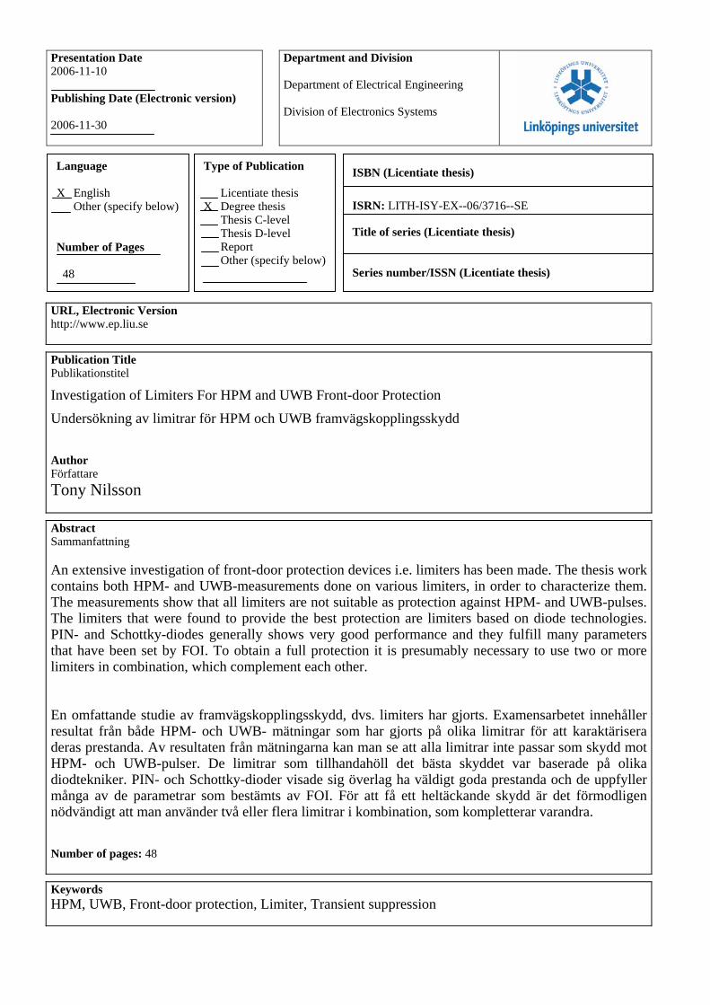
Presentation Date 2006-11-10 Publishing Date (Electronic version) 2006-11-30
Department and Division Department of Electrical Engineering Division of Electronics Systems
Language X English Other (specify below) Number of Pages 48
Type of Publication Licentiate thesis X Degree thesis Thesis C-level Thesis D-level Report Other (specify below)
ISBN (Licentiate thesis) ISRN: LITH-ISY-EX--06/3716--SE
Title of series (Licentiate thesis) Series number/ISSN (Licentiate thesis)
URL, Electronic Version http://www.ep.liu.se
Publication Title Publikationstitel
Investigation of Limiters For HPM and UWB Front-door Protection Undersökning av limitrar för HPM och UWB framvägskopplingsskydd Author Författare Tony Nilsson
Abstract Sammanfattning An extensive investigation of front-door protection devices i.e. limiters has been made. The thesis work contains both HPM- and UWB-measurements done on various limiters, in order to characterize them. The measurements show that all limiters are not suitable as protection against HPM- and UWB-pulses. The limiters that were found to provide the best protection are limiters based on diode technologies. PIN- and Schottky-diodes generally shows very good performance and they fulfill many parameters that have been set by FOI. To obtain a full protection it is presumably necessary to use two or more limiters in combination, which complement each other. En omfattande studie av framvägskopplingsskydd, dvs. limiters har gjorts. Examensarbetet innehåller resultat från både HPM- och UWB- mätningar som har gjorts på olika limitrar för att karaktärisera deras prestanda. Av resultaten från mätningarna kan man se att alla limitrar inte passar som skydd mot HPM- och UWB-pulser. De limitrar som tillhandahöll det bästa skyddet var baserade på olika diodtekniker. PIN- och Schottky-dioder visade sig överlag ha väldigt goda prestanda och de uppfyller många av de parametrar som bestämts av FOI. För att få ett heltäckande skydd är det förmodligen nödvändigt att man använder två eller flera limitrar i kombination, som kompletterar varandra. Number of pages: 48
Keywords HPM, UWB, Front-door protection, Limiter, Transient suppression

Table of Contents 1 Introduction................................................................................................................. 1
1.1 Project Goals and Specification .......................................................................... 1 1.1.1 Front-door protection Specification............................................................ 1
1.2 Threat Specification ............................................................................................ 2 1.2.1 HPM-pulses................................................................................................. 3 1.2.2 UWB-pulses................................................................................................ 3
1.3 Technical Terms.................................................................................................. 4 1.3.1 Threshold value........................................................................................... 4 1.3.2 Off-state ...................................................................................................... 5 1.3.3 On-state ....................................................................................................... 5 1.3.4 Response-time............................................................................................. 5 1.3.5 Recovery time ............................................................................................. 6 1.3.6 Front-door Coupling ................................................................................... 6 1.3.7 Back-door Coupling.................................................................................... 6
1.4 Front-door Protection Sub Groups...................................................................... 7 1.4.1 Clamping and Crowbaring.......................................................................... 7 1.4.2 Passive and Active Protection Devices....................................................... 7
2 Front-door Protection Devices and Technologies....................................................... 9 2.1 Gas Discharge Tubes (GDT) .............................................................................. 9 2.2 Air Gap Protection ............................................................................................ 10 2.3 Carbon Block Protection................................................................................... 10 2.4 Ferrite Limiter................................................................................................... 10 2.5 Diode Limiters .................................................................................................. 11
2.5.1 PN-diode Limiters..................................................................................... 11 2.5.2 Schottky-diode limiter .............................................................................. 12 2.5.3 PIN-Diode Limiters .................................................................................. 13
2.6 PUFET (Protectors against Ultra-Fast Electrical Transients)........................... 13 2.7 Metal OxideVaristor (MOV) ............................................................................ 14 2.8 Thyristor Limiter............................................................................................... 14 2.9 Selenium Cells .................................................................................................. 15 2.10 Research on Transient Protective Devices in GaAs MMIC ............................. 15
3 Selecting the Protection Device ................................................................................ 17 3.1 Hybrid Protection Circuits ................................................................................ 18
4 Measurements ........................................................................................................... 19 4.1 HPM Measurement Set-up................................................................................ 19
4.1.1 Calibration................................................................................................. 20 4.1.2 Measurements ........................................................................................... 20 4.1.3 Measurement Uncertainty......................................................................... 21
4.2 UWB Measurement Set-up ............................................................................... 21 4.2.1 Measurements ........................................................................................... 22 4.2.2 Measurement Uncertainty......................................................................... 23
5 Measurements and Results........................................................................................ 25 5.1 Omniyig OLP3140A......................................................................................... 25
5.1.1 HPM-Measurement Results ...................................................................... 25 5.1.2 UWB-Measurement Results ..................................................................... 26
5.2 Omniyig OLP3226A......................................................................................... 27
0
5.2.1 HPM-Measurement Results ...................................................................... 27
5.2.2 UWB-Measurement Results ..................................................................... 28 5.3 Multilayer Metal Oxide Varistor, EV18N0402L.............................................. 29
5.3.1 HPM-Measurement Results ...................................................................... 29 5.3.2 UWB-Measurement Results ..................................................................... 30
5.4 SRC CG75L...................................................................................................... 31 5.4.1 HPM-Measurement Results ...................................................................... 31 5.4.2 UWB-Measurement Results ..................................................................... 32
5.5 Microsemi GG77311-05 ................................................................................... 33 5.5.1 HPM-Measurement Results ...................................................................... 33 5.5.2 UWB-Measurement Results ..................................................................... 34
5.6 Microsemi GG77314-04 ................................................................................... 35 5.6.1 HPM-Measurement Results ...................................................................... 35 5.6.2 UWB-Measurement Results ..................................................................... 37
5.7 Triquint TGL2201-EPU.................................................................................... 37 5.7.1 HPM-Measurement Results ...................................................................... 38 5.7.2 UWB measurement results ....................................................................... 39
6 Summary and Conclusions ....................................................................................... 41 7 Future Work .............................................................................................................. 43 8 Acknowledgements................................................................................................... 45 9 References and Literature ......................................................................................... 47 1 Introduction The trend in today’s society is to integrate many electronic devices in all sorts of 1.1 Project Goals and Specification There are a large variety of different technologies which is used for front-door protection and many of these devices are today often available off-the-shelf. The aim with this thesis is to make an orientating survey of commercially available limiters and to get an understanding of how different protection technologies function. This was been done by measuring samples of various limiters and evaluate the corresponding results. Several parameters have been measured in order to characterize the limiters and thereby verify the ability to protect against UWB- and HPM-pulses. As a final result, the goal is to suggest which types of limiters that can be used for HPM and UWB font-door protection. 1.1.1 Front-door protection Specification
1
There are many specification parameters of the limiters that need to be met. It is likely that the restraints of all parameters can’t be fulfilled by one limiter. To meet the
1 Introduction The trend in today’s society is to integrate many electronic devices in all sorts of applications, more and more applications also tend to become wireless. This can be a growing problem and it tends to make the society more vulnerable to electrical interference such as IEMI (Intentional Electro Magnetic Interference) and HPEM (High Power Electromagnetic), e.g. HPM (High Power Microwaves) and UWB (Ultra Wide Band). Electric fields of high intensity can cause interference, operational failure or in the worst case severe physical damage to electronic equipment in some cases. It is difficult to protect from disturbances, however there are means for protection against the worst case scenario (physical damage). Shielding is one efficient way to protect the electronic circuits from electromagnetic interference, but when you have wireless applications you cannot completely shield them, due to antennas etc. Examples of such wireless applications are RADARs, WLANs (Wireless Local Area Networks) and cellular phones. In these cases you need other means for protection than shielding. This is where the front-door protection devices i.e. limiters enters the picture. This thesis work describes the process to sort out and evaluate suitable limiters that fulfil the FOI-specifications for front-door protection devices. This thesis involves all the steps, from investigation of commercially available limiters, measurements of important parameters in order to characterize the devices, and finally suggestions of suitable devices for protection of different application. 1.1 Project Goals and Specification There are a large variety of different technologies which is used for front-door protection and many of these devices are today often available off-the-shelf. The aim with this thesis is to make an orientating survey of commercially available limiters and to get an understanding of how different protection technologies function. This was been done by measuring samples of various limiters and evaluate the corresponding results. Several parameters have been measured in order to characterize the limiters and thereby verify the ability to protect against UWB- and HPM-pulses. As a final result, the goal is to suggest which types of limiters that can be used for HPM and UWB font-door protection. 1.1.1 Front-door protection Specification There are many specification parameters of the limiters that need to be met. It is likely that the restraints of all parameters can’t be fulfilled by one limiter. To meet the parameter requirements, limiters of different technologies will probably be combined, in this way would the technologies complement each other and constitute a good front-door protection. Below is a list of the parameter requirements considered to be important:
• Power durability, the limiter it self should be able to withstand repetitive pulses without permanent damage or degradation, a minimum of 50 dBm peak pulse, or 37 dBm CW (Continues Wave).
• Limiting levels, the limiting level is the maximum power that he limiter is letting
through, this level should be around 20 dBm in peak pulse or a leakage energy below the µJ-range (Depending on pulse width).
1
• Threshold level, this is the level when the limiter turns on and starts to limit the
input power, this level should be around 15 dBm.
• Response time, this is the time from when the pulse hits the limiter until it starts to limit the input power. This time should be less than 0.5 ns.
• Recovery time, this is the time from when the pulse ceases until the limiter returns
to normal operation, should be as short as possible, less than 1 µs.
• Insertion loss, this is signal losses due to component characteristics, this parameter should be as small as possible, less than 1.5 dB.
• Self capacitance, this is the capacitance of the limiter, when in normal operation.
This parameter should be as small as possible, less than 10 pF.
• Physical size is totally dependent on the application. This could be everything from integrated circuits to large N-type connector limiters.
As said before, generally no limiter will fulfil all these parameter requirements. Different types of limiters can be used in combinations in two or three stages. Where each stage consists of a different limiter technology. By using this technique the first stage limits the high power levels while the second stage cleans up remaining fast transients with fast rise times. This type of limiter is called a hybrid-circuit. 1.2 Threat Specification The regular types of weapons which are used for EW (Electronic Warfare) are often GPS- radio-, or RADAR-jammers and in some cases other more sophisticated technologies. These EW-weapons are designed with good target knowledge and their function is to temporarily disturb critical target systems. The detailed target knowledge can be such things as frequency-bands, signal modulation etc. This results in EW-weapons which radiates only moderate power levels into the front-door path of the target. HPEM-weapons, such as HPM (High Power Microwaves) and UWB (Ultra Wide Band) on the other hand use more of a brute force compared to EW-weapons. The HPEM-weapons can be divided into two main categories, HPM and UWB. This will be further explained in section 1.2.1 and 1.2.2. The main intention of a HPEM-weapon is to cause massive functional upsets or permanent damage of critical target systems or components. The HPEM-weapons radiates electromagnetic fields with extremely high levels, which may result in both back-door and front-door coupling to the target. This type of weapon requires very little target knowledge.
2
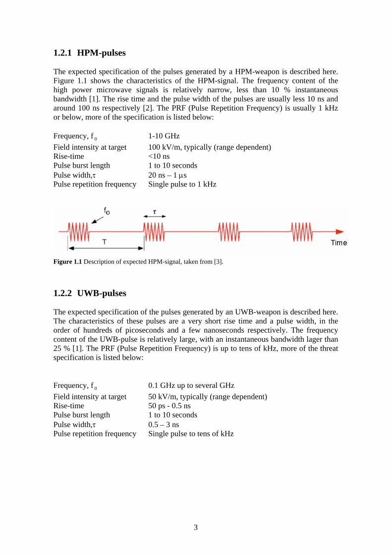
1.2.1 HPM-pulses The expected specification of the pulses generated by a HPM-weapon is described here. Figure 1.1 shows the characteristics of the HPM-signal. The frequency content of the high power microwave signals is relatively narrow, less than 10 % instantaneous bandwidth [1]. The rise time and the pulse width of the pulses are usually less 10 ns and around 100 ns respectively [2]. The PRF (Pulse Repetition Frequency) is usually 1 kHz or below, more of the specification is listed below: Frequency, f 1-10 GHz 0
Field intensity at target 100 kV/m, typically (range dependent) Rise-time <10 ns Pulse burst length 1 to 10 seconds Pulse width,τ 20 ns – 1 µs Pulse repetition frequency Single pulse to 1 kHz
Figure 1.1 Description of expected HPM-signal, taken from [3].
1.2.2 UWB-pulses The expected specification of the pulses generated by an UWB-weapon is described here. The characteristics of these pulses are a very short rise time and a pulse width, in the order of hundreds of picoseconds and a few nanoseconds respectively. The frequency content of the UWB-pulse is relatively large, with an instantaneous bandwidth lager than 25 % [1]. The PRF (Pulse Repetition Frequency) is up to tens of kHz, more of the threat specification is listed below: Frequency, f 0.1 GHz up to several GHz 0
Field intensity at target 50 kV/m, typically (range dependent) Rise-time 50 ps - 0.5 ns Pulse burst length 1 to 10 seconds Pulse width,τ 0.5 – 3 ns Pulse repetition frequency Single pulse to tens of kHz
3
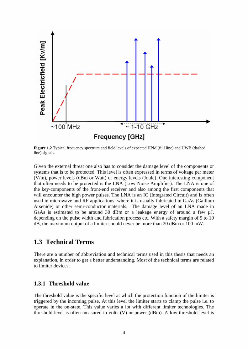
Figure 1.2 Typical frequency spectrum and field levels of expected HPM (full line) and UWB (dashed line) signals.
Given the external threat one also has to consider the damage level of the components or systems that is to be protected. This level is often expressed in terms of voltage per meter (V/m), power levels (dBm or Watt) or energy levels (Joule). One interesting component that often needs to be protected is the LNA (Low Noise Amplifier). The LNA is one of the key-components of the front-end receiver and also among the first components that will encounter the high power pulses. The LNA is an IC (Integrated Circuit) and is often used in microwave and RF applications, where it is usually fabricated in GaAs (Gallium Arsenide) or other semi-conductor materials. The damage level of an LNA made in GaAs is estimated to be around 30 dBm or a leakage energy of around a few µJ, depending on the pulse width and fabrication process etc. With a safety margin of 5 to 10 dB, the maximum output of a limiter should never be more than 20 dBm or 100 mW. 1.3 Technical Terms There are a number of abbreviation and technical terms used in this thesis that needs an explanation, in order to get a better understanding. Most of the technical terms are related to limiter devices. 1.3.1 Threshold value The threshold value is the specific level at which the protection function of the limiter is triggered by the incoming pulse. At this level the limiter starts to clamp the pulse i.e. to operate in the on-state. This value varies a lot with different limiter technologies. The threshold level is often measured in volts (V) or power (dBm). A low threshold level is
4
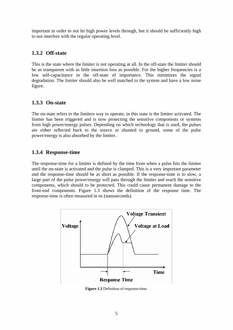
important in order to not let high power levels through, but it should be sufficiently high to not interfere with the regular operating level. 1.3.2 Off-state This is the state where the limiter is not operating at all. In the off-state the limiter should be as transparent with as little insertion loss as possible. For the higher frequencies is a low self-capacitance in the off-state of importance. This minimizes the signal degradation. The limiter should also be well matched to the system and have a low noise figure. 1.3.3 On-state The on-state refers to the limiters way to operate, in this state is the limiter activated. The limiter has been triggered and is now protecting the sensitive components or systems from high power/energy pulses. Depending on which technology that is used, the pulses are either reflected back to the source or shunted to ground, some of the pulse power/energy is also absorbed by the limiter. 1.3.4 Response-time The response-time for a limiter is defined by the time from when a pulse hits the limiter until the on-state is activated and the pulse is clamped. This is a very important parameter and the response-time should be as short as possible. If the response-time is to slow, a large part of the pulse power/energy will pass through the limiter and reach the sensitive components, which should to be protected. This could cause permanent damage to the front-end components. Figure 1.3 shows the definition of the response time. The response-time is often measured in ns (nanoseconds).
Figure 1.3 Definition of response-time.
5
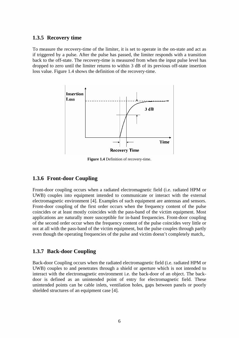
1.3.5 Recovery time To measure the recovery-time of the limiter, it is set to operate in the on-state and act as if triggered by a pulse. After the pulse has passed, the limiter responds with a transition back to the off-state. The recovery-time is measured from when the input pulse level has dropped to zero until the limiter returns to within 3 dB of its previous off-state insertion loss value. Figure 1.4 shows the definition of the recovery-time.
Figure 1.4 Definition of recovery-time.
1.3.6 Front-door Coupling Front-door coupling occurs when a radiated electromagnetic field (i.e. radiated HPM or UWB) couples into equipment intended to communicate or interact with the external electromagnetic environment [4]. Examples of such equipment are antennas and sensors. Front-door coupling of the first order occurs when the frequency content of the pulse coincides or at least mostly coincides with the pass-band of the victim equipment. Most applications are naturally more susceptible for in-band frequencies. Front-door coupling of the second order occur when the frequency content of the pulse coincides very little or not at all with the pass-band of the victim equipment, but the pulse couples through partly even though the operating frequencies of the pulse and victim doesn’t completely match,. 1.3.7 Back-door Coupling Back-door Coupling occurs when the radiated electromagnetic field (i.e. radiated HPM or UWB) couples to and penetrates through a shield or aperture which is not intended to interact with the electromagnetic environment i.e. the back-door of an object. The back-door is defined as an unintended point of entry for electromagnetic field. These unintended points can be cable inlets, ventilation holes, gaps between panels or poorly shielded structures of an equipment case [4].
6
1.4 Front-door Protection Sub Groups Limiters i.e. front-door protection devices can be divided into several sub groups. This depends on the behaviour and the technology on which the limiter is based on. Two of the sub groups are clamping and crowbaring devices, these two groups refers to the limiting mechanism of the device. The limiters can also be further divided into subgroups, active and passive devices, which refer to how the device is activated, [5]. 1.4.1 Clamping and Crowbaring The two main types of limiters, clamping devices and crowbaring devices, the name of these to groups refers to the way the devices limits the pulses. The clamping device limits the pulse by changing its impedance. As soon as the pulse exceeds the threshold level of the limiter, it starts to conduct and clamps the pulse to a safe level. The clamping response provides a low impedance path between the signal line and ground. The top of the pulse is clipped off and the pulse is clamped to a safe level near the nominal operating voltage. Diode-limiters and MOVs (Metal Oxide Varistors) are examples of clamping devices. A crowbaring device uses a switching mechanism and starts to conduct when the high power pulse exceeds a certain threshold level. When the device starts to conduct, it short-circuits the pulse to ground and the voltage level drops until it reaches zero. The limiter then returns to the off-state when the pulse has passed. The recovery time of a crowbaring device is in general longer compared to clamping devices, due to its low impedance. It allows the flow of substantially large surge currents, which remains in the device [5]. Crowbaring devices can also in general handle larger voltages and currents without suffering from breakdown, compared to clamping devices, Examples of crowbaring devices are GDTs (Gas Discharge Tubes), and air gaps. 1.4.2 Passive and Active Protection Devices Limiters can also be divided into passive and active types of protection devices [6]. More simplified is a passive protection device self-activated. It needs no external control signals or power supply to perform its protection operation. Most of the protection devices available are passive. Active protection devices on the other hand need external control signals or power supply to perform their protection operation. An active protection device is often some kind of switch. The advantages of active devices are in general faster recovery times and that a very small amount of the energy is transmitted to the protected circuitry. On of the drawbacks with this type of protection devices is that they don’t provide any protection when the device is turned off or if the controls signal fails. The further investigation of limiters in this thesis will be focused on passive devices.
7

8
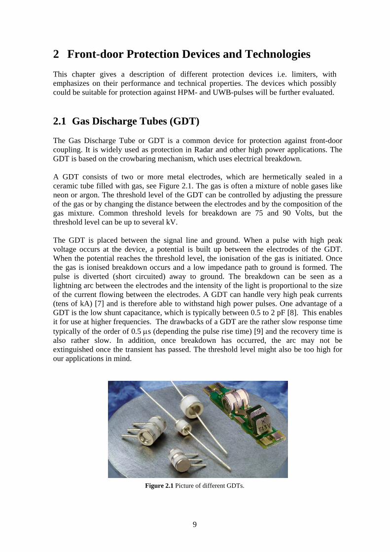
2 Front-door Protection Devices and Technologies This chapter gives a description of different protection devices i.e. limiters, with emphasizes on their performance and technical properties. The devices which possibly could be suitable for protection against HPM- and UWB-pulses will be further evaluated. 2.1 Gas Discharge Tubes (GDT) The Gas Discharge Tube or GDT is a common device for protection against front-door coupling. It is widely used as protection in Radar and other high power applications. The GDT is based on the crowbaring mechanism, which uses electrical breakdown. A GDT consists of two or more metal electrodes, which are hermetically sealed in a ceramic tube filled with gas, see Figure 2.1. The gas is often a mixture of noble gases like neon or argon. The threshold level of the GDT can be controlled by adjusting the pressure of the gas or by changing the distance between the electrodes and by the composition of the gas mixture. Common threshold levels for breakdown are 75 and 90 Volts, but the threshold level can be up to several kV. The GDT is placed between the signal line and ground. When a pulse with high peak voltage occurs at the device, a potential is built up between the electrodes of the GDT. When the potential reaches the threshold level, the ionisation of the gas is initiated. Once the gas is ionised breakdown occurs and a low impedance path to ground is formed. The pulse is diverted (short circuited) away to ground. The breakdown can be seen as a lightning arc between the electrodes and the intensity of the light is proportional to the size of the current flowing between the electrodes. A GDT can handle very high peak currents (tens of kA) [7] and is therefore able to withstand high power pulses. One advantage of a GDT is the low shunt capacitance, which is typically between 0.5 to 2 pF [8]. This enables it for use at higher frequencies. The drawbacks of a GDT are the rather slow response time typically of the order of 0.5 µs (depending the pulse rise time) [9] and the recovery time is also rather slow. In addition, once breakdown has occurred, the arc may not be extinguished once the transient has passed. The threshold level might also be too high for our applications in mind.
Figure 2.1 Picture of different GDTs.
9
The lifetime of a GDT is finite and depends on the number of pulses and the size of them. For pulses with high peak levels, the GDT will only withstand a few cycles of successful protection. The GDT could be an interesting device to use in a combination with other types of limiters as a hybrid protection device. Primarily it could be suitable as a first stage in a protection circuit and protect from high power levels. 2.2 Air Gap Protection The air gap protection consists of two metal electrodes, which are separated by a thin gap of air. The principle of this device is much the same as for the GDTs. When a pulse with a voltage level high enough hits the air gap, a potential between the electrodes is built up. When the potential is high enough, the threshold voltage is reached and breakdown between the electrodes occurs in the air. This kind of protection device is not hermetically sealed and is therefore working at atmospheric pressure and also under the influence of different environmental conditions. This can lead to corrosion of the electrodes, which may results in degradation of the overall performance of the air gap. The degradation is mainly seen as an increase of the threshold voltage and as an increase of the response-time. However the response-time can be as fast as 5 ps, theoretically [10]. This type of protection method is not suitable for protection of low voltage circuits due to the high threshold level, but maybe it could be used as a first stage protection, handling high power levels. Breakdown in antenna slots is a protection technique that has been investigated at FOI. The basic principle is that the air in the antenna slot is ionised by high energy microwave pulses. The geometric features of the slot and the dielectric properties of the antenna substrate decide the threshold level. More information can be found in [11] and [12]. If air gaps can be integrated as a natural part of slot antennas it would be a good advantage, due to that it doesn’t degrade the signal performance. 2.3 Carbon Block Protection The Carbon block protection used to be a very common from of protection against voltage pulses. It was usually used as a primary protection, due to its ability to handle large transients. The principle of the carbon block is similar to the principle of the GDT and the air gap. The carbon block consists of a pair of carbon elements, which is separated by a thin gap (~ 0.1 mm) of air. The carbon elements of the device are not hermetically sealed, which results in similar performance degradation, as for the air gap protection. When high power pulses hits the carbon block a potential is built up between the carbon elements. When the potential reaches the threshold level a breakdown is triggered, and the pulse is shunted to ground. One of the drawbacks of this component is that it is relatively unpredictable, the threshold level can vary between 400 to 600 Volts [13]. Due to its properties it is considered not suitable as protection for low voltage circuits. 2.4 Ferrite Limiter The ferrite limiter is usually integrated in waveguides or snapped on to a cable. Figure 2.2 show a picture of two different kinds ferrite limiters. In the case with the waveguide the ferrite material is mounted on the inside walls of the waveguide and is biased using
10
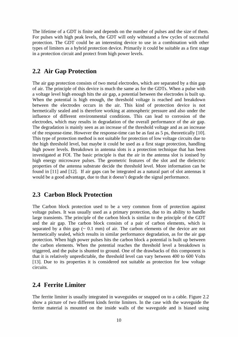
permanent magnets. The limiter acts like a piece of dielectrically loaded waveguide in the off-state [6]. When in the off-state, the electrons of the ferrite are precessing around the magnetic field lines. This state is kept until a pulse hits the limiter and the threshold value of the limiter is reached. Then the energy of the pulse that exceeded the threshold level is coupled into the precession motion of the electrons. The energy is absorbed by the ferrite and converted to heat. One advantage is the unlimited life time and that this is an all solid state device. On the other hand can a ferrite limiter not be used for high microwave frequencies. In the case when the ferrite limiter is snapped on to a cable, it is usually used for protection from pulses and disturbances with a frequency below 2.5 GHz.
Figure 2.2 Picture of snap-on limiter (left) and waveguide limiter (right).
2.5 Diode Limiters There are a variety of different diode limiters. The diode limiter is a component which clamps the pulse, in particular pulses with low currents and fast rise times. The threshold level of a diode can be adjusted by changing the level of the doping or by introducing an intrinsic region between the P and N Regions. In order to use diode limiters for higher frequencies the junction capacitance must be kept low, this results in a comparably small junction area. When a pulse hits the diode-limiter, all of the shunted energy is forced to pass through the small junction of the doped areas. The energy is converted to heat, which can be very intense for pulses with high energy. This lack of ability to handle high currents is a limitation of the diode limiter. The diode limiter might be degraded or destroyed if exposed to pulses with high power/energy content. 2.5.1 PN-diode Limiters There are two mechanisms of breakdown for the PN-diode, zener- and avalanche-breakdown. Figure 2.3 show PN-diode limiters with axial leads.
11
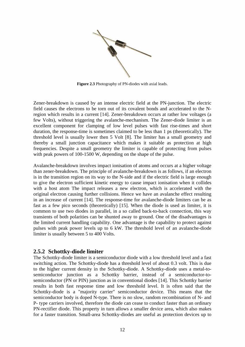
Figure 2.3 Photography of PN-diodes with axial leads.
Zener-breakdown is caused by an intense electric field at the PN-junction. The electric field causes the electrons to be torn out of its covalent bonds and accelerated to the N-region which results in a current [14]. Zener-breakdown occurs at rather low voltages (a few Volts), without triggering the avalanche-mechanism. The Zener-diode limiter is an excellent component for clamping of low level pulses with fast rise-times and short duration, the response-time is sometimes claimed to be less than 1 ps (theoretically). The threshold level is usually lower then 5 Volt [8]. The limiter has a small geometry and thereby a small junction capacitance which makes it suitable as protection at high frequencies. Despite a small geometry the limiter is capable of protecting from pulses with peak powers of 100-1500 W, depending on the shape of the pulse. Avalanche-breakdown involves impact ionisation of atoms and occurs at a higher voltage than zener-breakdown. The principle of avalanche-breakdown is as follows, if an electron is in the transition region on its way to the N-side and if the electric field is large enough to give the electron sufficient kinetic energy to cause impact ionisation when it collides with a host atom The impact releases a new electron, which is accelerated with the original electron causing further collisions. Hence we have an avalanche effect resulting in an increase of current [14]. The response-time for avalanche-diode limiters can be as fast as a few pico seconds (theoretically) [15]. When the diode is used as limiter, it is common to use two diodes in parallel, in a so called back-to-back connection, this way transients of both polarities can be shunted away to ground. One of the disadvantages is the limited current handling capability. One advantage is the capability to protect against pulses with peak power levels up to 6 kW. The threshold level of an avalanche-diode limiter is usually between 5 to 400 Volts. 2.5.2 Schottky-diode limiter The Schottky-diode limiter is a semiconductor diode with a low threshold level and a fast switching action. The Schottky-diode has a threshold level of about 0.3 volt. This is due to the higher current density in the Schottky-diode. A Schottky-diode uses a metal-to-semiconductor junction as a Schottky barrier, instead of a semiconductor-to-semiconductor (PN or PIN) junction as in conventional diodes [14]. This Schottky barrier results in both fast response time and low threshold level. It is often said that the Schottky-diode is a "majority carrier" semiconductor device. This means that the semiconductor body is doped N-type. There is no slow, random recombination of N- and P- type carriers involved, therefore the diode can cease to conduct faster than an ordinary PN-rectifier diode. This property in turn allows a smaller device area, which also makes for a faster transition. Small-area Schottky-diodes are useful as protection devices up to
12
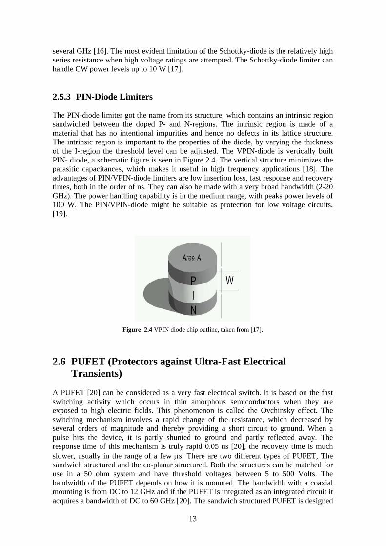
several GHz [16]. The most evident limitation of the Schottky-diode is the relatively high series resistance when high voltage ratings are attempted. The Schottky-diode limiter can handle CW power levels up to 10 W [17]. 2.5.3 PIN-Diode Limiters The PIN-diode limiter got the name from its structure, which contains an intrinsic region sandwiched between the doped P- and N-regions. The intrinsic region is made of a material that has no intentional impurities and hence no defects in its lattice structure. The intrinsic region is important to the properties of the diode, by varying the thickness of the I-region the threshold level can be adjusted. The VPIN-diode is vertically built PIN- diode, a schematic figure is seen in Figure 2.4. The vertical structure minimizes the parasitic capacitances, which makes it useful in high frequency applications [18]. The advantages of PIN/VPIN-diode limiters are low insertion loss, fast response and recovery times, both in the order of ns. They can also be made with a very broad bandwidth (2-20 GHz). The power handling capability is in the medium range, with peaks power levels of 100 W. The PIN/VPIN-diode might be suitable as protection for low voltage circuits, [19].
Figure 2.4 VPIN diode chip outline, taken from [17].
2.6 PUFET (Protectors against Ultra-Fast Electrical
Transients) A PUFET [20] can be considered as a very fast electrical switch. It is based on the fast switching activity which occurs in thin amorphous semiconductors when they are exposed to high electric fields. This phenomenon is called the Ovchinsky effect. The switching mechanism involves a rapid change of the resistance, which decreased by several orders of magnitude and thereby providing a short circuit to ground. When a pulse hits the device, it is partly shunted to ground and partly reflected away. The response time of this mechanism is truly rapid 0.05 ns [20], the recovery time is much slower, usually in the range of a few µs. There are two different types of PUFET, The sandwich structured and the co-planar structured. Both the structures can be matched for use in a 50 ohm system and have threshold voltages between 5 to 500 Volts. The bandwidth of the PUFET depends on how it is mounted. The bandwidth with a coaxial mounting is from DC to 12 GHz and if the PUFET is integrated as an integrated circuit it acquires a bandwidth of DC to 60 GHz [20]. The sandwich structured PUFET is designed
13
to handle pulses of 1 to 2 kVolt, with a rise time of 1 ns. The other type of PUFET, the co-planar structured is designed to withstand pulses up to 1 kVolt, with a rise time of 0.3 ns. Both types of PUFETs have the disadvantage of finite lifetime. The lifetime depends on the amount of energy in the pulse and the number of pulses. The PUFET is unfortunately not commercially available due export restriction and other complications. 2.7 Metal OxideVaristor (MOV) The metal oxide varistor is a semiconductor component which is made of metal oxide, usually zink oxide. Figure 2.5 show MOVs with axial leads, MOVs are also available in other packaging for surface mounting. The MOV works as a voltage controlled resistance with a non-linear voltage/current dependence. The MOV has a very high resistance when operating in its normal working range. When the MOV is exposed to high power/energy pulses exceeding the threshold level (10 to 1500 Volt), the resistance is rapidly decreased and the MOV provides a low impedance path to ground which shunts the pulse to ground. The response-time is claimed to be as low as 0.1 ns [21]. Due to the design of the MOV, it clamps pulses of both polarities. The MOV also has a relatively good power handling capability. The lifetime of a MOV is finite and depends on the size and number of pulses. One disadvantage is that with increasing number of transients the electrical properties are degraded [8]. It also has a moderate self capacitance (~100 pf or more), which might restraint it for use in high frequency applications.
Figure 2.5 Picture of metal oxide varistors with axial leads.
2.8 Thyristor Limiter The thyristor is based on a crowbaring technology, which use the avalanche-mechanism [22]. The regular operating voltage is between 12 up to several hundreds of Volts. The capability of shunting pulses depends on the size as well as structure of the component. During regular operating conditions the limiter acts as transparent. The threshold level is usually 20% to 30% higher than the regular operating voltage. When a pulse hits the thyristor, it switches to the on-state, a current starts to flow and the pulse is shunted to ground. In order to return to the off-state the current through the device must drop below the minimum holding current. The advantages of the thyristor limiter are large current handling capability at a low threshold levels and that it has a low capacitance which makes it suitable for higher frequencies. The disadvantages on the other hand include a
14
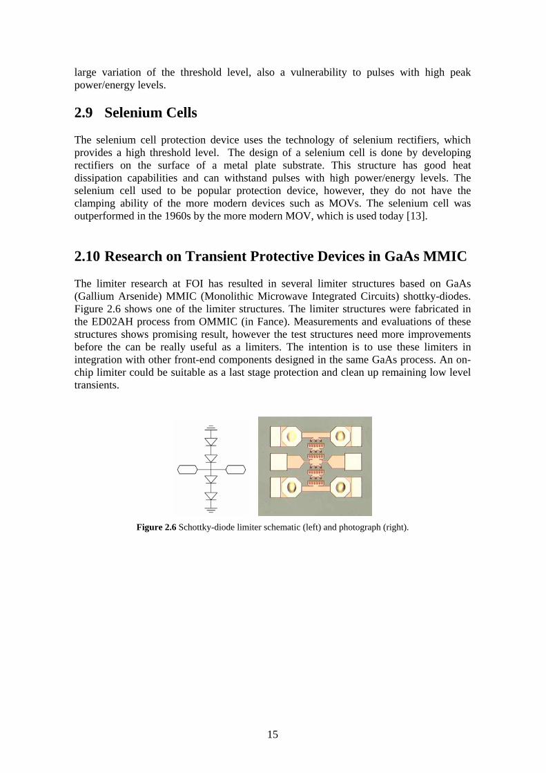
large variation of the threshold level, also a vulnerability to pulses with high peak power/energy levels. 2.9 Selenium Cells The selenium cell protection device uses the technology of selenium rectifiers, which provides a high threshold level. The design of a selenium cell is done by developing rectifiers on the surface of a metal plate substrate. This structure has good heat dissipation capabilities and can withstand pulses with high power/energy levels. The selenium cell used to be popular protection device, however, they do not have the clamping ability of the more modern devices such as MOVs. The selenium cell was outperformed in the 1960s by the more modern MOV, which is used today [13]. 2.10 Research on Transient Protective Devices in GaAs MMIC The limiter research at FOI has resulted in several limiter structures based on GaAs (Gallium Arsenide) MMIC (Monolithic Microwave Integrated Circuits) shottky-diodes. Figure 2.6 shows one of the limiter structures. The limiter structures were fabricated in the ED02AH process from OMMIC (in Fance). Measurements and evaluations of these structures shows promising result, however the test structures need more improvements before the can be really useful as a limiters. The intention is to use these limiters in integration with other front-end components designed in the same GaAs process. An on-chip limiter could be suitable as a last stage protection and clean up remaining low level transients.
Figure 2.6 Schottky-diode limiter schematic (left) and photograph (right).
15

16
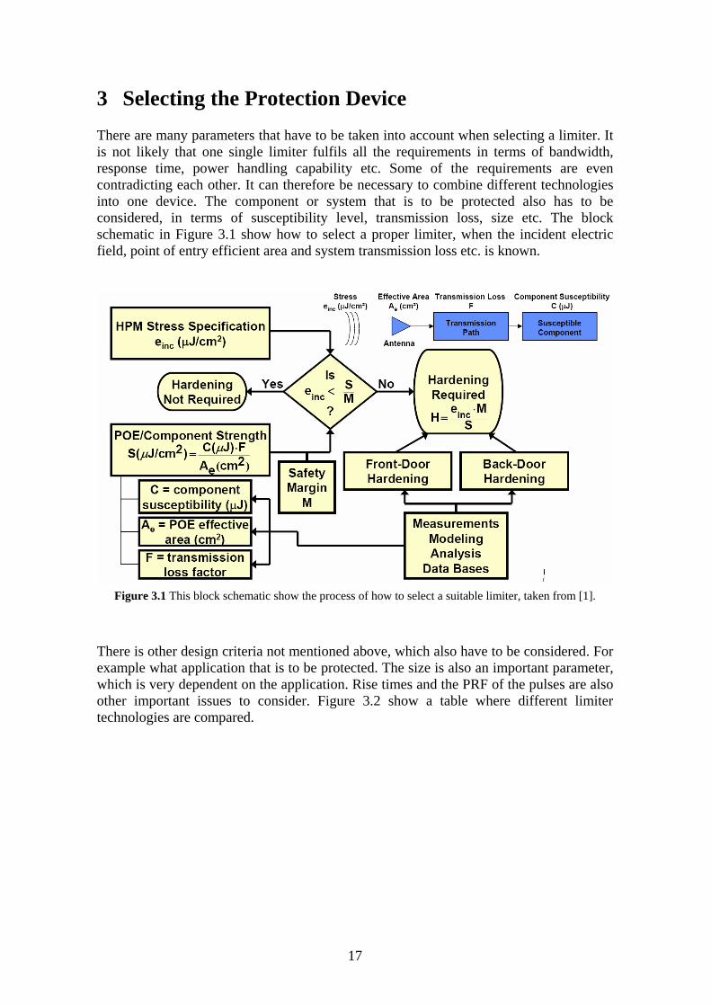
3 Selecting the Protection Device There are many parameters that have to be taken into account when selecting a limiter. It is not likely that one single limiter fulfils all the requirements in terms of bandwidth, response time, power handling capability etc. Some of the requirements are even contradicting each other. It can therefore be necessary to combine different technologies into one device. The component or system that is to be protected also has to be considered, in terms of susceptibility level, transmission loss, size etc. The block schematic in Figure 3.1 show how to select a proper limiter, when the incident electric field, point of entry efficient area and system transmission loss etc. is known.
Figure 3.1 This block schematic show the process of how to select a suitable limiter, taken from [1].
There is other design criteria not mentioned above, which also have to be considered. For example what application that is to be protected. The size is also an important parameter, which is very dependent on the application. Rise times and the PRF of the pulses are also other important issues to consider. Figure 3.2 show a table where different limiter technologies are compared.
17
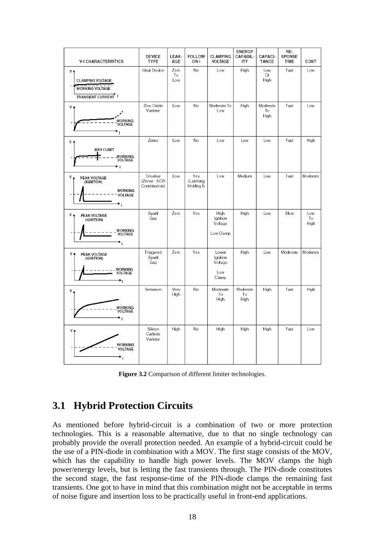
Figure 3.2 Comparison of different limiter technologies.
3.1 Hybrid Protection Circuits As mentioned before hybrid-circuit is a combination of two or more protection technologies. This is a reasonable alternative, due to that no single technology can probably provide the overall protection needed. An example of a hybrid-circuit could be the use of a PIN-diode in combination with a MOV. The first stage consists of the MOV, which has the capability to handle high power levels. The MOV clamps the high power/energy levels, but is letting the fast transients through. The PIN-diode constitutes the second stage, the fast response-time of the PIN-diode clamps the remaining fast transients. One got to have in mind that this combination might not be acceptable in terms of noise figure and insertion loss to be practically useful in front-end applications.
18
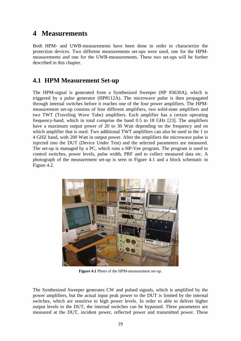
4 Measurements Both HPM- and UWB-measurements have been done in order to characterize the protection devices. Two different measurements set-ups were used, one for the HPM-measurements and one for the UWB-measurements. These two set-ups will be further described in this chapter. 4.1 HPM Measurement Set-up The HPM-signal is generated from a Synthesized Sweeper (HP 83630A), which is triggered by a pulse generator (HP8112A). The microwave pulse is then propagated through internal switches before it reaches one of the four power amplifiers. The HPM-measurement set-up consists of four different amplifiers, two solid-state amplifiers and two TWT (Traveling Wave Tube) amplifiers. Each amplifier has a certain operating frequency-band, which in total comprise the band 0.5 to 18 GHz [23]. The amplifiers have a maximum output power of 20 to 30 Watt depending on the frequency and on which amplifier that is used. Two additional TWT amplifiers can also be used in the 1 to 4 GHZ band, with 200 Watt in output power. After the amplifiers the microwave pulse is injected into the DUT (Device Under Test) and the selected parameters are measured. The set-up is managed by a PC, which runs a HP-Vee program. The program is used to control switches, power levels, pulse width, PRF and to collect measured data etc. A photograph of the measurement set-up is seen in Figure 4.1 and a block schematic in Figure 4.2.
Figure 4.1 Photo of the HPM-measurement set-up.
The Synthesized Sweeper generates CW and pulsed signals, which is amplified by the power amplifiers, but the actual input peak power to the DUT is limited by the internal switches, which are sensitive to high power levels. In order to able to deliver higher output levels to the DUT, the internal switches can be bypassed. Three parameters are measured at the DUT, incident power, reflected power and transmitted power. These
19
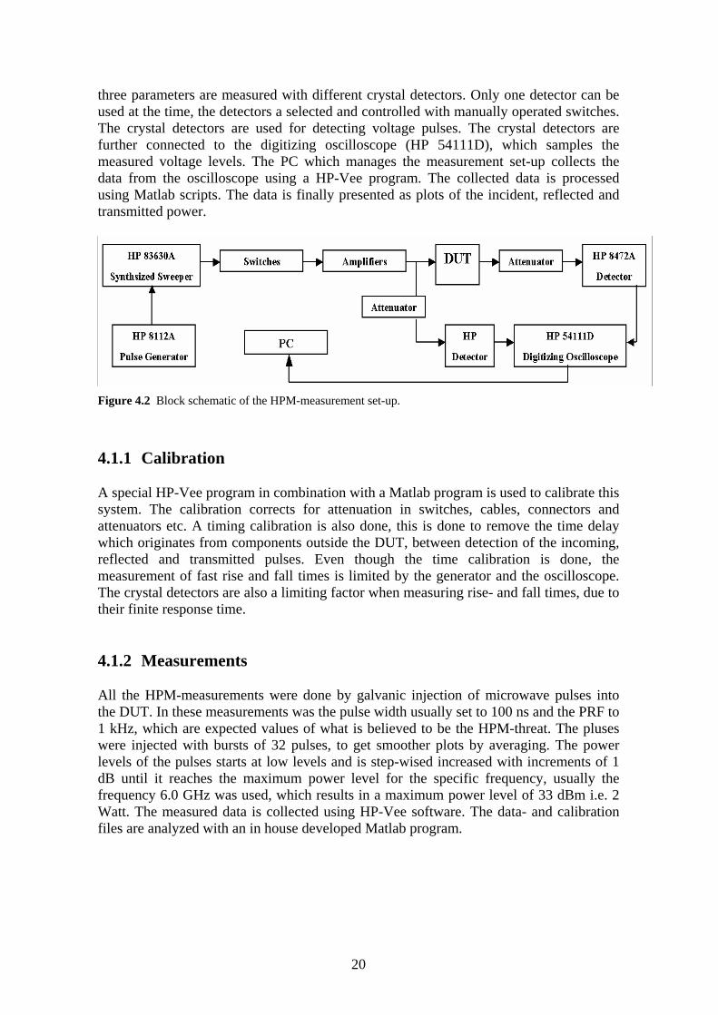
three parameters are measured with different crystal detectors. Only one detector can be used at the time, the detectors a selected and controlled with manually operated switches. The crystal detectors are used for detecting voltage pulses. The crystal detectors are further connected to the digitizing oscilloscope (HP 54111D), which samples the measured voltage levels. The PC which manages the measurement set-up collects the data from the oscilloscope using a HP-Vee program. The collected data is processed using Matlab scripts. The data is finally presented as plots of the incident, reflected and transmitted power.
Figure 4.2 Block schematic of the HPM-measurement set-up.
4.1.1 Calibration A special HP-Vee program in combination with a Matlab program is used to calibrate this system. The calibration corrects for attenuation in switches, cables, connectors and attenuators etc. A timing calibration is also done, this is done to remove the time delay which originates from components outside the DUT, between detection of the incoming, reflected and transmitted pulses. Even though the time calibration is done, the measurement of fast rise and fall times is limited by the generator and the oscilloscope. The crystal detectors are also a limiting factor when measuring rise- and fall times, due to their finite response time. 4.1.2 Measurements All the HPM-measurements were done by galvanic injection of microwave pulses into the DUT. In these measurements was the pulse width usually set to 100 ns and the PRF to 1 kHz, which are expected values of what is believed to be the HPM-threat. The pluses were injected with bursts of 32 pulses, to get smoother plots by averaging. The power levels of the pulses starts at low levels and is step-wised increased with increments of 1 dB until it reaches the maximum power level for the specific frequency, usually the frequency 6.0 GHz was used, which results in a maximum power level of 33 dBm i.e. 2 Watt. The measured data is collected using HP-Vee software. The data- and calibration files are analyzed with an in house developed Matlab program.
20
4.1.3 Measurement Uncertainty The measurement uncertainty for the HPM-measurement set-up has been estimated. Several parameters have been taken into account, for example losses in cables, connection and switches etc. The estimated uncertainty for the HPM power levels is 0.5 dB. The oscilloscope has about 1 % in measurement uncertainty. The detectors used for the measurements have finite rise time, 3.5 ns, which may change the shape of the pulse. Further investigation of the measurement uncertainty will be done. 4.2 UWB Measurement Set-up The UWB-measurements set-up consists of a PGS402 pulse source from Power Spectra. A HP 8112A pulse source was used to trigger the PGS402. This source generates UWB- pulses, with very short rise-time and pulse width. Special attenuators are placed before and after the DUT. These high voltage attenuators (from Barth Electronics) are used to regulate the power delivered to the DUT, attenuators where also used between the DUT and the oscilloscope to limit the voltage at the oscilloscope input to 5 V (maximum input level to the oscilloscope) when needed. The pulse source generates a 400 Volt uni-polar pulse with a rise-time of about 300 ps and a pulse width of about 1 ns into a 50Ω load. The pulse is measured with a fast Tektronix TDS 6604 Digital oscilloscope (6 GHz analog bandwidth, 20 GSample/s). A photograph of the measurement set-up can be seen in Figure 4.3 and a block schematic in Figure 4.4.
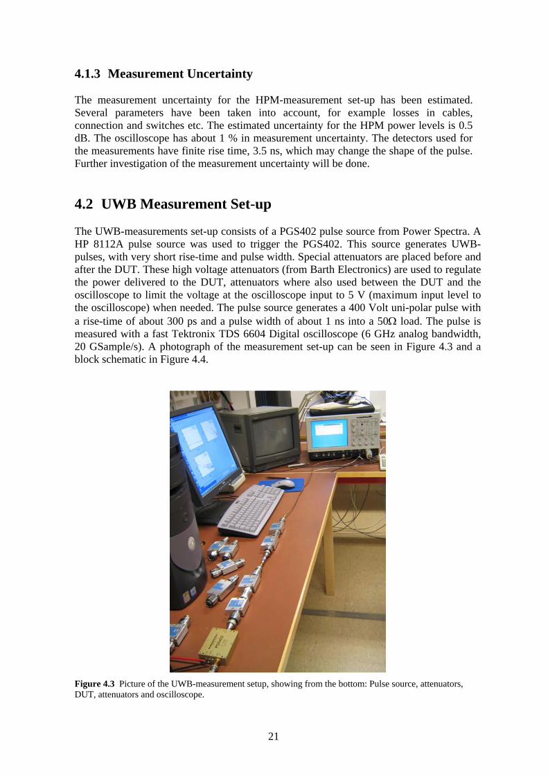
Figure 4.3 Picture of the UWB-measurement setup, showing from the bottom: Pulse source, attenuators, DUT, attenuators and oscilloscope.
21
The UWB measurements are useful for characterizing the general response to fast pulses and to investigate the possible spike leakage. It is of great interest to investigate the spike leakage of a DUT, which occurs due to the finite response time of the limiter. From these measurements can the maximum power/energy leakage be determined. All the limiters were subjected to this type of test and the results are presented in chapter 5. The maximum PRF of the PGS402 is 50 kHz but in the measurements a 33 Hz PRF was used, mainly to enhance the lifetime of the pulse source. The power spectrum of the output pulse from the PGS402 can be seen in Figure 4.5.
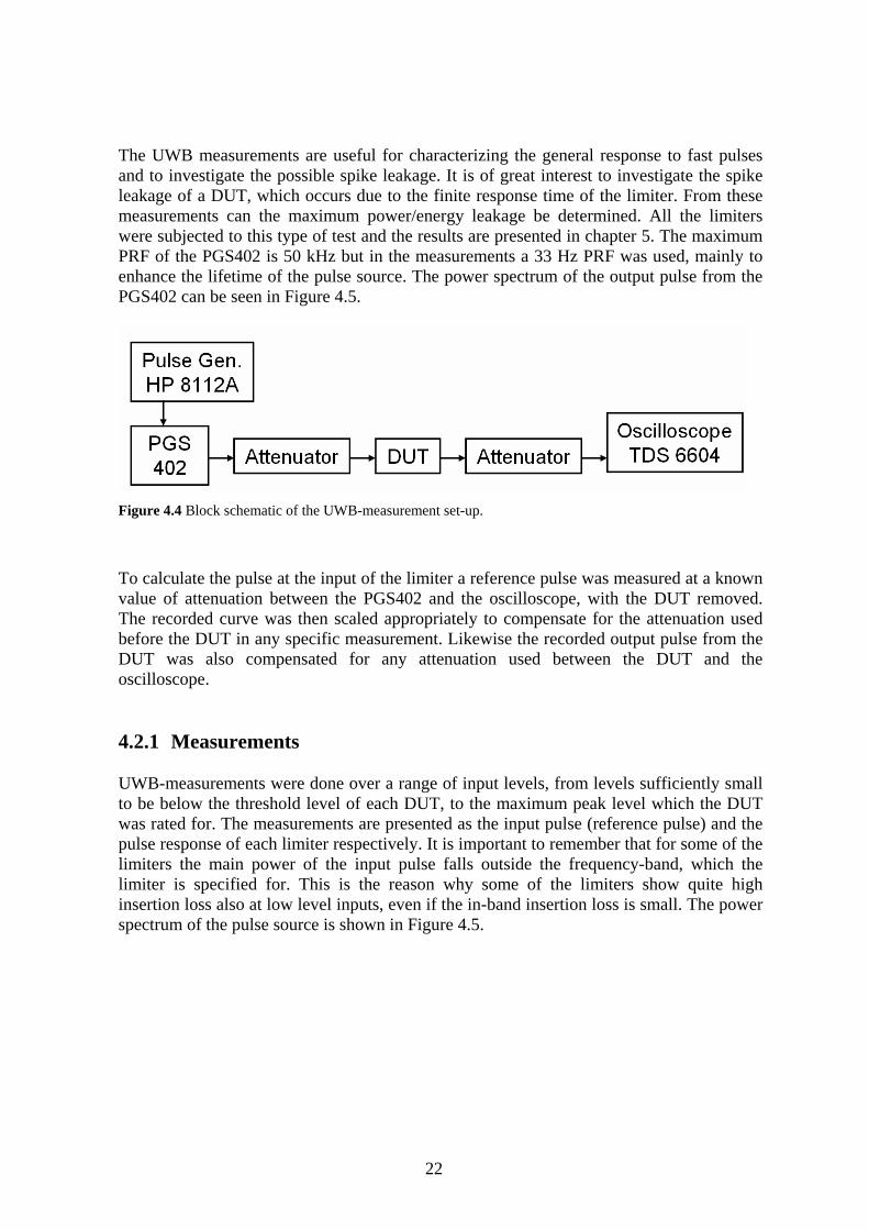
Figure 4.4 Block schematic of the UWB-measurement set-up.
To calculate the pulse at the input of the limiter a reference pulse was measured at a known value of attenuation between the PGS402 and the oscilloscope, with the DUT removed. The recorded curve was then scaled appropriately to compensate for the attenuation used before the DUT in any specific measurement. Likewise the recorded output pulse from the DUT was also compensated for any attenuation used between the DUT and the oscilloscope. 4.2.1 Measurements UWB-measurements were done over a range of input levels, from levels sufficiently small to be below the threshold level of each DUT, to the maximum peak level which the DUT was rated for. The measurements are presented as the input pulse (reference pulse) and the pulse response of each limiter respectively. It is important to remember that for some of the limiters the main power of the input pulse falls outside the frequency-band, which the limiter is specified for. This is the reason why some of the limiters show quite high insertion loss also at low level inputs, even if the in-band insertion loss is small. The power spectrum of the pulse source is shown in Figure 4.5.
22
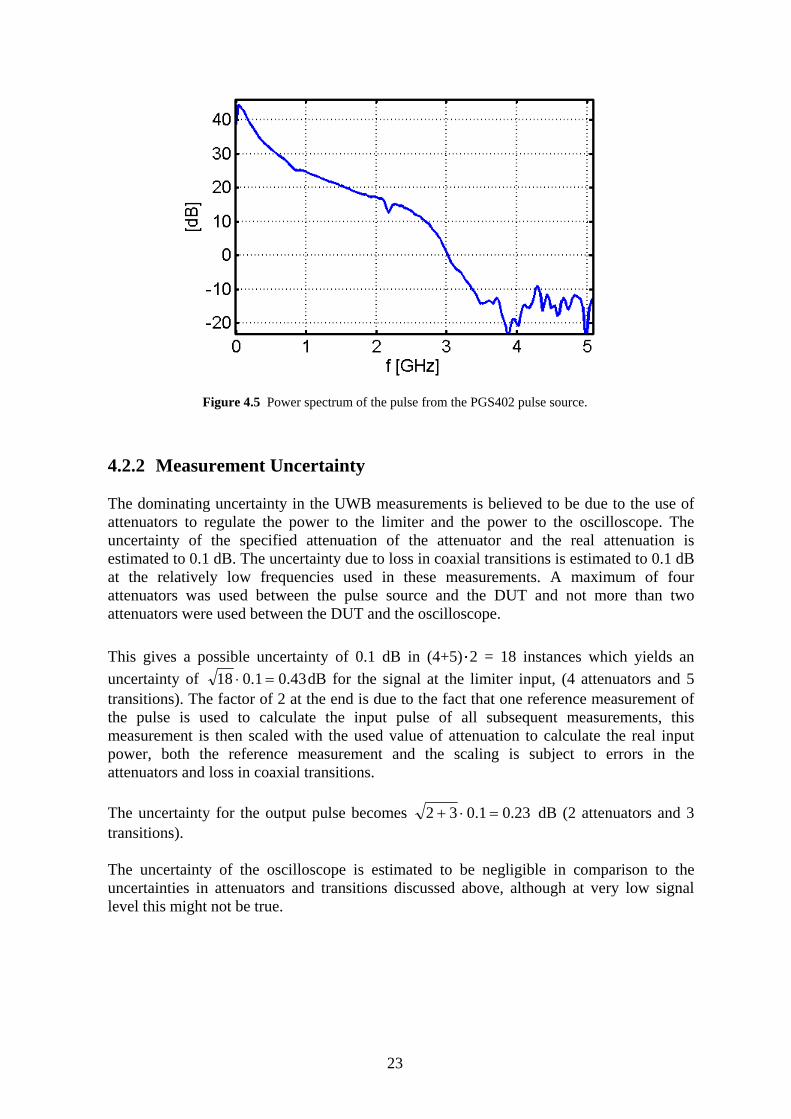
Figure 4.5 Power spectrum of the pulse from the PGS402 pulse source.
4.2.2 Measurement Uncertainty The dominating uncertainty in the UWB measurements is believed to be due to the use of attenuators to regulate the power to the limiter and the power to the oscilloscope. The uncertainty of the specified attenuation of the attenuator and the real attenuation is estimated to 0.1 dB. The uncertainty due to loss in coaxial transitions is estimated to 0.1 dB at the relatively low frequencies used in these measurements. A maximum of four attenuators was used between the pulse source and the DUT and not more than two attenuators were used between the DUT and the oscilloscope. This gives a possible uncertainty of 0.1 dB in (4+5)·2 = 18 instances which yields an uncertainty of 43.01.018 =⋅ dB for the signal at the limiter input, (4 attenuators and 5 transitions). The factor of 2 at the end is due to the fact that one reference measurement of the pulse is used to calculate the input pulse of all subsequent measurements, this measurement is then scaled with the used value of attenuation to calculate the real input power, both the reference measurement and the scaling is subject to errors in the attenuators and loss in coaxial transitions. The uncertainty for the output pulse becomes 23.01.032 =⋅+ dB (2 attenuators and 3 transitions). The uncertainty of the oscilloscope is estimated to be negligible in comparison to the uncertainties in attenuators and transitions discussed above, although at very low signal level this might not be true.
23

24
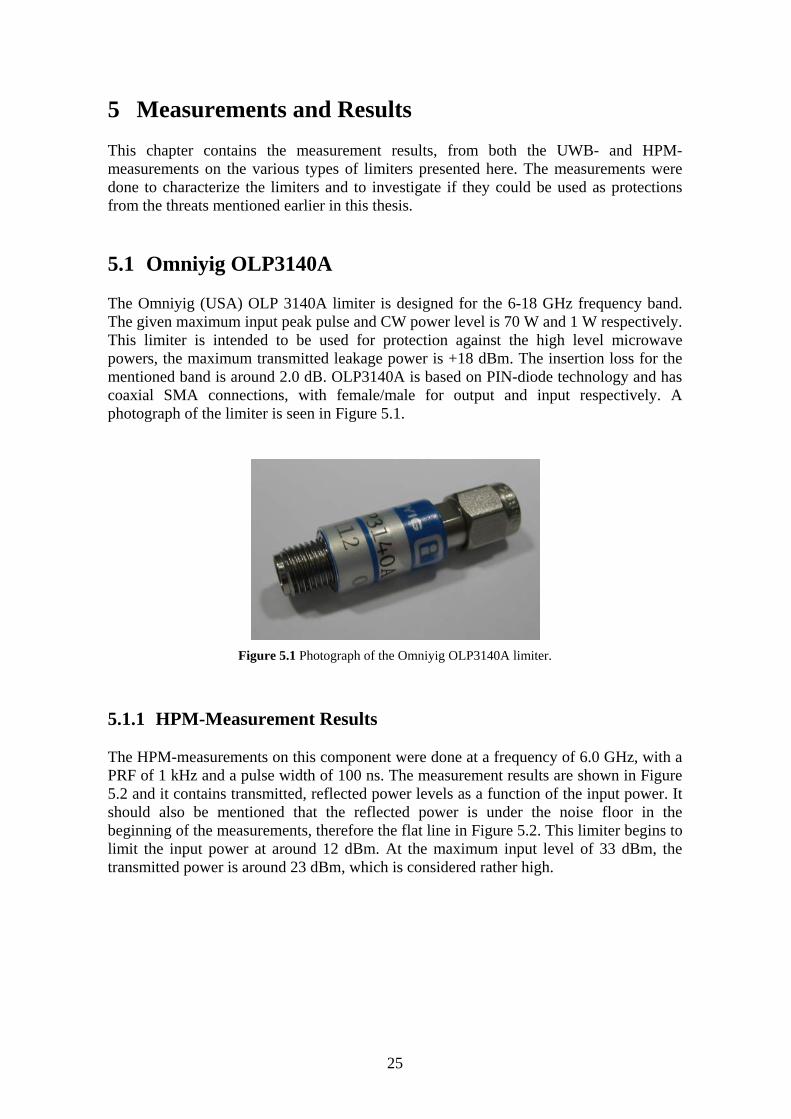
5 Measurements and Results This chapter contains the measurement results, from both the UWB- and HPM- measurements on the various types of limiters presented here. The measurements were done to characterize the limiters and to investigate if they could be used as protections from the threats mentioned earlier in this thesis. 5.1 Omniyig OLP3140A The Omniyig (USA) OLP 3140A limiter is designed for the 6-18 GHz frequency band. The given maximum input peak pulse and CW power level is 70 W and 1 W respectively. This limiter is intended to be used for protection against the high level microwave powers, the maximum transmitted leakage power is +18 dBm. The insertion loss for the mentioned band is around 2.0 dB. OLP3140A is based on PIN-diode technology and has coaxial SMA connections, with female/male for output and input respectively. A photograph of the limiter is seen in Figure 5.1.
Figure 5.1 Photograph of the Omniyig OLP3140A limiter.
5.1.1 HPM-Measurement Results The HPM-measurements on this component were done at a frequency of 6.0 GHz, with a PRF of 1 kHz and a pulse width of 100 ns. The measurement results are shown in Figure 5.2 and it contains transmitted, reflected power levels as a function of the input power. It should also be mentioned that the reflected power is under the noise floor in the beginning of the measurements, therefore the flat line in Figure 5.2. This limiter begins to limit the input power at around 12 dBm. At the maximum input level of 33 dBm, the transmitted power is around 23 dBm, which is considered rather high.
25
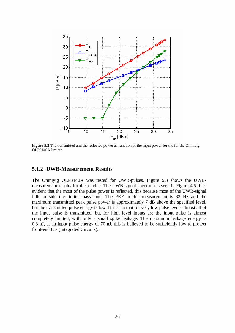
Figure 5.2 The transmitted and the reflected power as function of the input power for the for the Omniyig OLP3140A limiter.
5.1.2 UWB-Measurement Results The Omniyig OLP3140A was tested for UWB-pulses. Figure 5.3 shows the UWB- measurement results for this device. The UWB-signal spectrum is seen in Figure 4.5. It is evident that the most of the pulse power is reflected, this because most of the UWB-signal falls outside the limiter pass-band. The PRF in this measurement is 33 Hz and the maximum transmitted peak pulse power is approximately 7 dB above the specified level, but the transmitted pulse energy is low. It is seen that for very low pulse levels almost all of the input pulse is transmitted, but for high level inputs are the input pulse is almost completely limited, with only a small spike leakage. The maximum leakage energy is 0.3 nJ, at an input pulse energy of 70 nJ, this is believed to be sufficiently low to protect front-end ICs (Integrated Circuits).
26
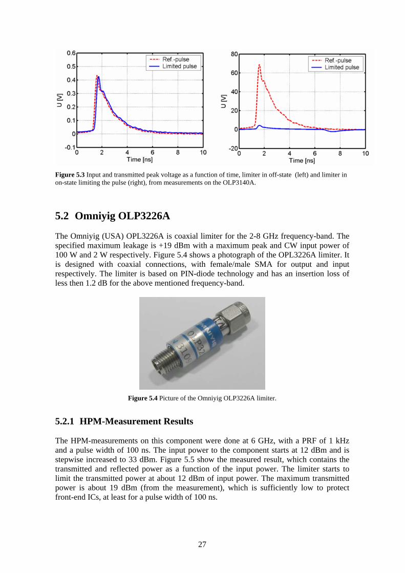
Figure 5.3 Input and transmitted peak voltage as a function of time, limiter in off-state (left) and limiter in on-state limiting the pulse (right), from measurements on the OLP3140A.
5.2 Omniyig OLP3226A The Omniyig (USA) OPL3226A is coaxial limiter for the 2-8 GHz frequency-band. The specified maximum leakage is +19 dBm with a maximum peak and CW input power of 100 W and 2 W respectively. Figure 5.4 shows a photograph of the OPL3226A limiter. It is designed with coaxial connections, with female/male SMA for output and input respectively. The limiter is based on PIN-diode technology and has an insertion loss of less then 1.2 dB for the above mentioned frequency-band.
Figure 5.4 Picture of the Omniyig OLP3226A limiter.
5.2.1 HPM-Measurement Results The HPM-measurements on this component were done at 6 GHz, with a PRF of 1 kHz and a pulse width of 100 ns. The input power to the component starts at 12 dBm and is stepwise increased to 33 dBm. Figure 5.5 show the measured result, which contains the transmitted and reflected power as a function of the input power. The limiter starts to limit the transmitted power at about 12 dBm of input power. The maximum transmitted power is about 19 dBm (from the measurement), which is sufficiently low to protect front-end ICs, at least for a pulse width of 100 ns.
27
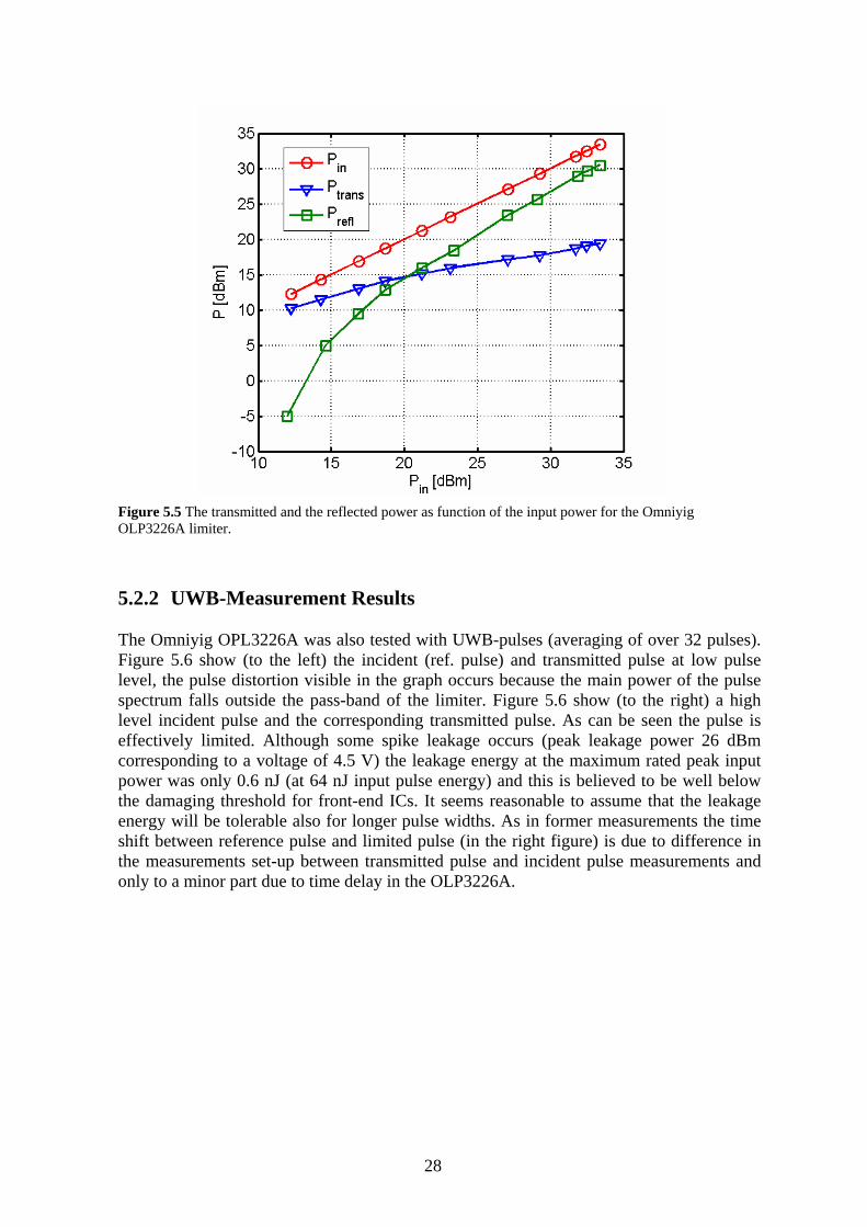
Figure 5.5 The transmitted and the reflected power as function of the input power for the Omniyig OLP3226A limiter.
5.2.2 UWB-Measurement Results The Omniyig OPL3226A was also tested with UWB-pulses (averaging of over 32 pulses). Figure 5.6 show (to the left) the incident (ref. pulse) and transmitted pulse at low pulse level, the pulse distortion visible in the graph occurs because the main power of the pulse spectrum falls outside the pass-band of the limiter. Figure 5.6 show (to the right) a high level incident pulse and the corresponding transmitted pulse. As can be seen the pulse is effectively limited. Although some spike leakage occurs (peak leakage power 26 dBm corresponding to a voltage of 4.5 V) the leakage energy at the maximum rated peak input power was only 0.6 nJ (at 64 nJ input pulse energy) and this is believed to be well below the damaging threshold for front-end ICs. It seems reasonable to assume that the leakage energy will be tolerable also for longer pulse widths. As in former measurements the time shift between reference pulse and limited pulse (in the right figure) is due to difference in the measurements set-up between transmitted pulse and incident pulse measurements and only to a minor part due to time delay in the OLP3226A.
28
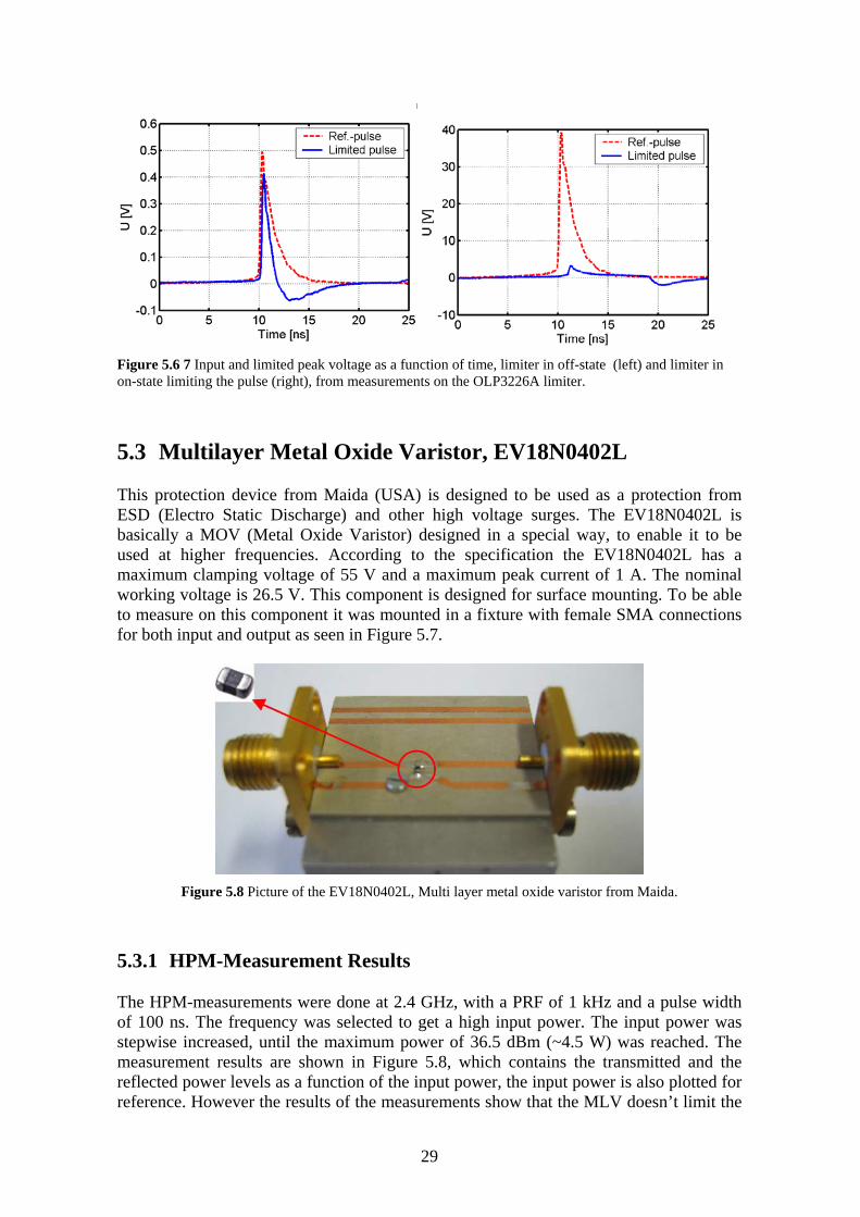
Figure 5.6 7 Input and limited peak voltage as a function of time, limiter in off-state (left) and limiter in on-state limiting the pulse (right), from measurements on the OLP3226A limiter.
5.3 Multilayer Metal Oxide Varistor, EV18N0402L This protection device from Maida (USA) is designed to be used as a protection from ESD (Electro Static Discharge) and other high voltage surges. The EV18N0402L is basically a MOV (Metal Oxide Varistor) designed in a special way, to enable it to be used at higher frequencies. According to the specification the EV18N0402L has a maximum clamping voltage of 55 V and a maximum peak current of 1 A. The nominal working voltage is 26.5 V. This component is designed for surface mounting. To be able to measure on this component it was mounted in a fixture with female SMA connections for both input and output as seen in Figure 5.7.
Figure 5.8 Picture of the EV18N0402L, Multi layer metal oxide varistor from Maida.
5.3.1 HPM-Measurement Results The HPM-measurements were done at 2.4 GHz, with a PRF of 1 kHz and a pulse width of 100 ns. The frequency was selected to get a high input power. The input power was stepwise increased, until the maximum power of 36.5 dBm (~4.5 W) was reached. The measurement results are shown in Figure 5.8, which contains the transmitted and the reflected power levels as a function of the input power, the input power is also plotted for reference. However the results of the measurements show that the MLV doesn’t limit the
29
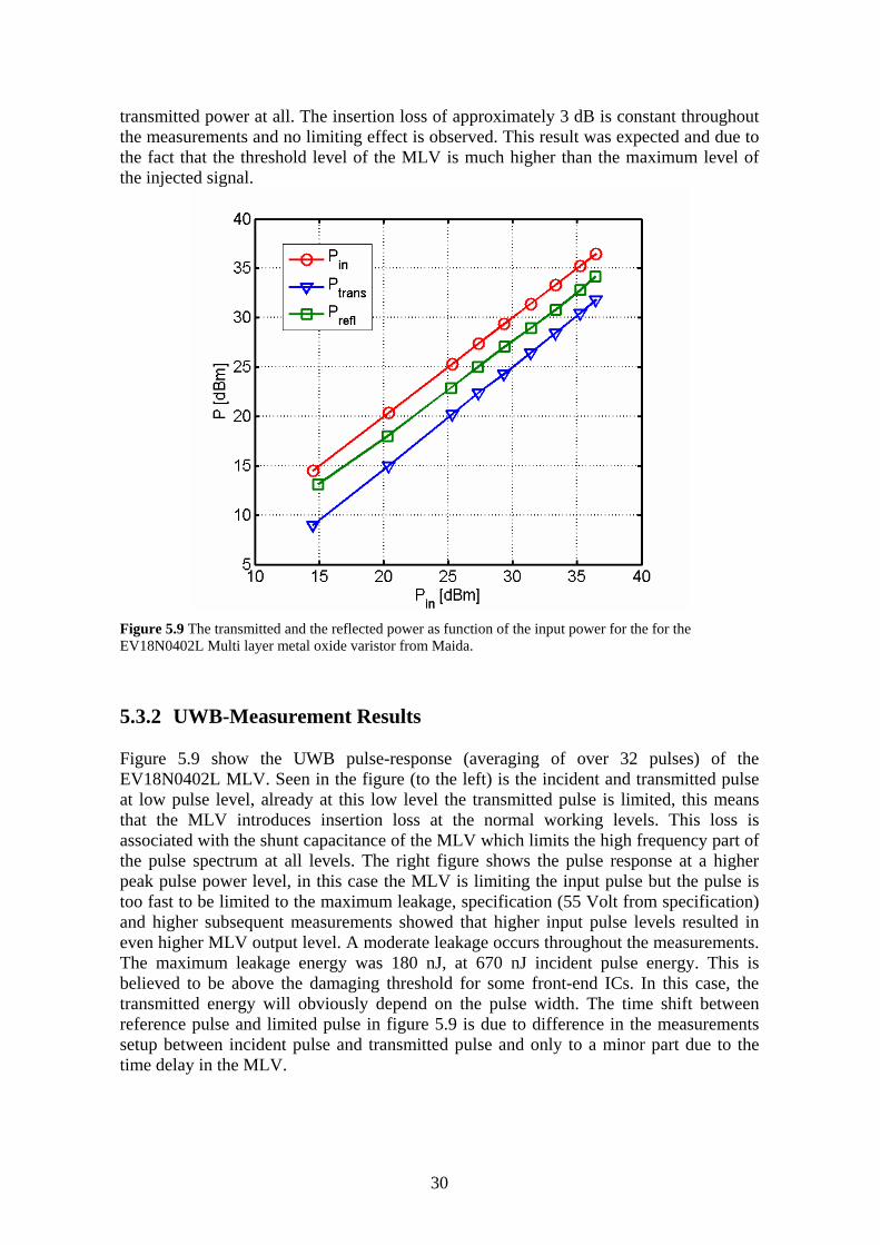
transmitted power at all. The insertion loss of approximately 3 dB is constant throughout the measurements and no limiting effect is observed. This result was expected and due to the fact that the threshold level of the MLV is much higher than the maximum level of the injected signal.
Figure 5.9 The transmitted and the reflected power as function of the input power for the for the EV18N0402L Multi layer metal oxide varistor from Maida.
5.3.2 UWB-Measurement Results Figure 5.9 show the UWB pulse-response (averaging of over 32 pulses) of the EV18N0402L MLV. Seen in the figure (to the left) is the incident and transmitted pulse at low pulse level, already at this low level the transmitted pulse is limited, this means that the MLV introduces insertion loss at the normal working levels. This loss is associated with the shunt capacitance of the MLV which limits the high frequency part of the pulse spectrum at all levels. The right figure shows the pulse response at a higher peak pulse power level, in this case the MLV is limiting the input pulse but the pulse is too fast to be limited to the maximum leakage, specification (55 Volt from specification) and higher subsequent measurements showed that higher input pulse levels resulted in even higher MLV output level. A moderate leakage occurs throughout the measurements. The maximum leakage energy was 180 nJ, at 670 nJ incident pulse energy. This is believed to be above the damaging threshold for some front-end ICs. In this case, the transmitted energy will obviously depend on the pulse width. The time shift between reference pulse and limited pulse in figure 5.9 is due to difference in the measurements setup between incident pulse and transmitted pulse and only to a minor part due to the time delay in the MLV.
30
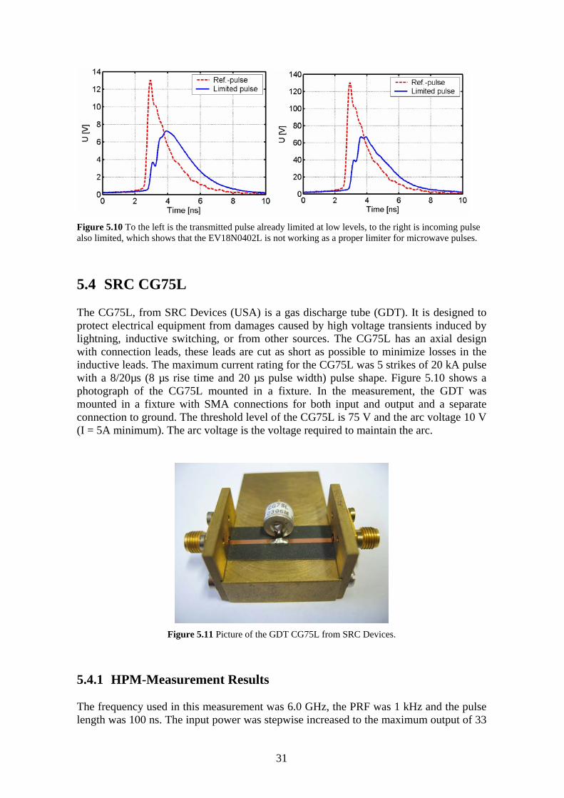
Figure 5.10 To the left is the transmitted pulse already limited at low levels, to the right is incoming pulse also limited, which shows that the EV18N0402L is not working as a proper limiter for microwave pulses.
5.4 SRC CG75L The CG75L, from SRC Devices (USA) is a gas discharge tube (GDT). It is designed to protect electrical equipment from damages caused by high voltage transients induced by lightning, inductive switching, or from other sources. The CG75L has an axial design with connection leads, these leads are cut as short as possible to minimize losses in the inductive leads. The maximum current rating for the CG75L was 5 strikes of 20 kA pulse with a 8/20µs (8 µs rise time and 20 µs pulse width) pulse shape. Figure 5.10 shows a photograph of the CG75L mounted in a fixture. In the measurement, the GDT was mounted in a fixture with SMA connections for both input and output and a separate connection to ground. The threshold level of the CG75L is 75 V and the arc voltage 10 V (I = 5A minimum). The arc voltage is the voltage required to maintain the arc.
Figure 5.11 Picture of the GDT CG75L from SRC Devices.
5.4.1 HPM-Measurement Results The frequency used in this measurement was 6.0 GHz, the PRF was 1 kHz and the pulse length was 100 ns. The input power was stepwise increased to the maximum output of 33
31
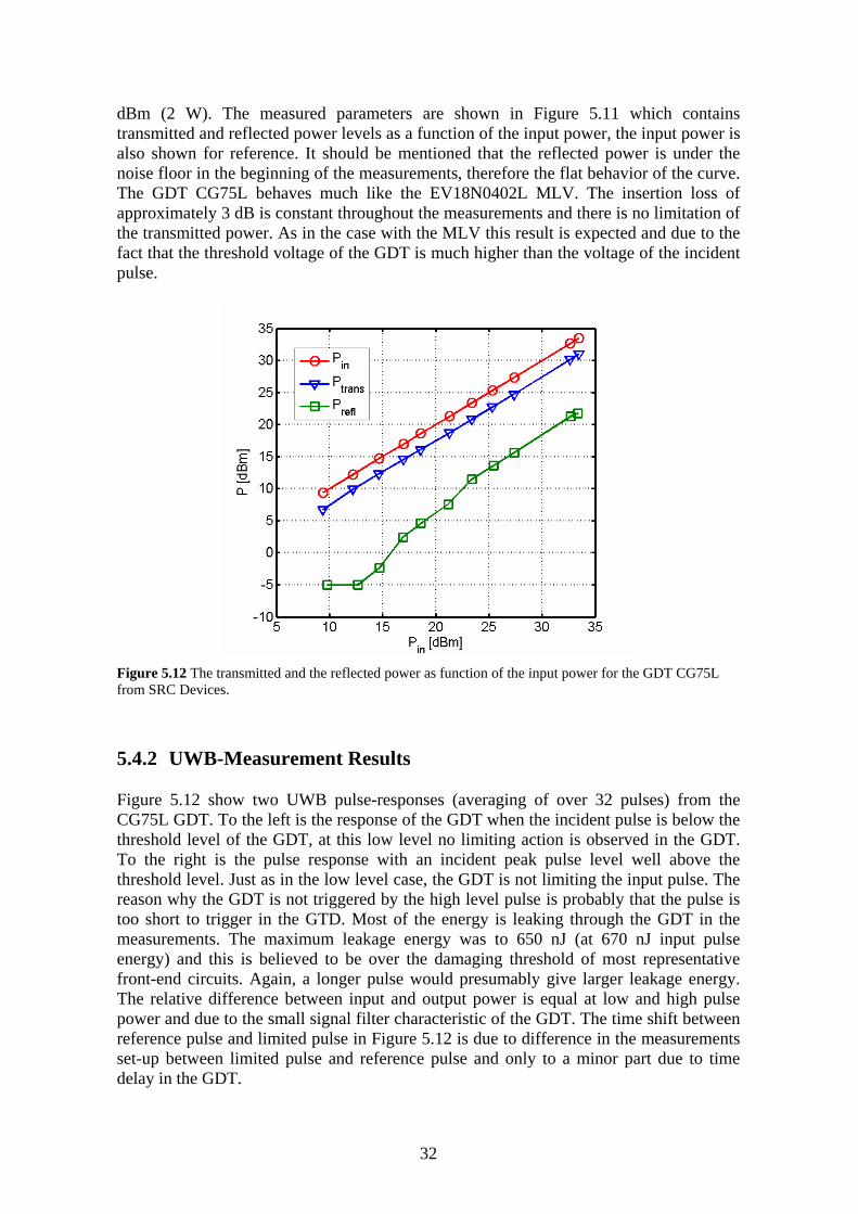
dBm (2 W). The measured parameters are shown in Figure 5.11 which contains transmitted and reflected power levels as a function of the input power, the input power is also shown for reference. It should be mentioned that the reflected power is under the noise floor in the beginning of the measurements, therefore the flat behavior of the curve. The GDT CG75L behaves much like the EV18N0402L MLV. The insertion loss of approximately 3 dB is constant throughout the measurements and there is no limitation of the transmitted power. As in the case with the MLV this result is expected and due to the fact that the threshold voltage of the GDT is much higher than the voltage of the incident pulse.
Figure 5.12 The transmitted and the reflected power as function of the input power for the GDT CG75L from SRC Devices.
5.4.2 UWB-Measurement Results Figure 5.12 show two UWB pulse-responses (averaging of over 32 pulses) from the CG75L GDT. To the left is the response of the GDT when the incident pulse is below the threshold level of the GDT, at this low level no limiting action is observed in the GDT. To the right is the pulse response with an incident peak pulse level well above the threshold level. Just as in the low level case, the GDT is not limiting the input pulse. The reason why the GDT is not triggered by the high level pulse is probably that the pulse is too short to trigger in the GTD. Most of the energy is leaking through the GDT in the measurements. The maximum leakage energy was to 650 nJ (at 670 nJ input pulse energy) and this is believed to be over the damaging threshold of most representative front-end circuits. Again, a longer pulse would presumably give larger leakage energy. The relative difference between input and output power is equal at low and high pulse power and due to the small signal filter characteristic of the GDT. The time shift between reference pulse and limited pulse in Figure 5.12 is due to difference in the measurements set-up between limited pulse and reference pulse and only to a minor part due to time delay in the GDT.
32
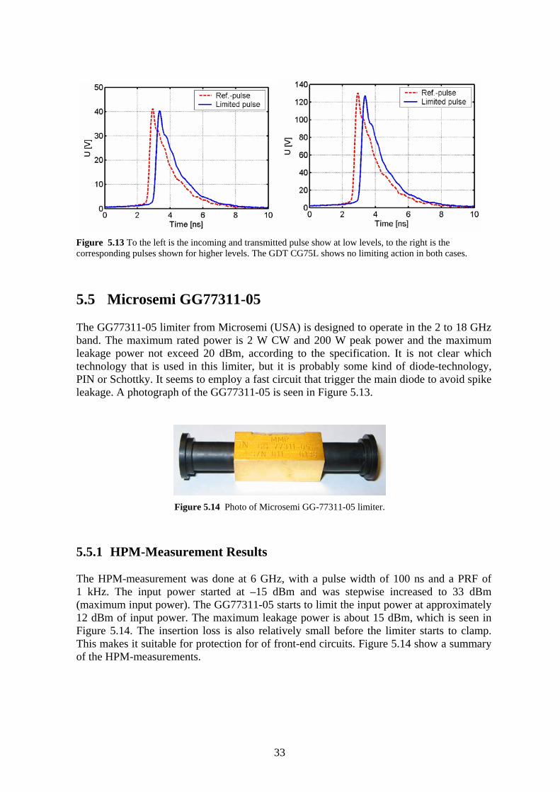
Figure 5.13 To the left is the incoming and transmitted pulse show at low levels, to the right is the corresponding pulses shown for higher levels. The GDT CG75L shows no limiting action in both cases.
5.5 Microsemi GG77311-05 The GG77311-05 limiter from Microsemi (USA) is designed to operate in the 2 to 18 GHz band. The maximum rated power is 2 W CW and 200 W peak power and the maximum leakage power not exceed 20 dBm, according to the specification. It is not clear which technology that is used in this limiter, but it is probably some kind of diode-technology, PIN or Schottky. It seems to employ a fast circuit that trigger the main diode to avoid spike leakage. A photograph of the GG77311-05 is seen in Figure 5.13.
Figure 5.14 Photo of Microsemi GG-77311-05 limiter.
5.5.1 HPM-Measurement Results The HPM-measurement was done at 6 GHz, with a pulse width of 100 ns and a PRF of 1 kHz. The input power started at –15 dBm and was stepwise increased to 33 dBm (maximum input power). The GG77311-05 starts to limit the input power at approximately 12 dBm of input power. The maximum leakage power is about 15 dBm, which is seen in Figure 5.14. The insertion loss is also relatively small before the limiter starts to clamp. This makes it suitable for protection for of front-end circuits. Figure 5.14 show a summary of the HPM-measurements.
33
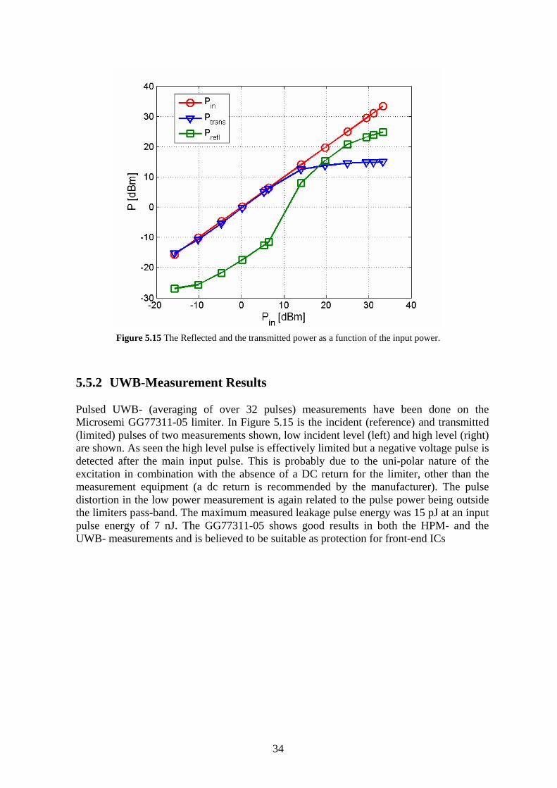
Figure 5.15 The Reflected and the transmitted power as a function of the input power.
5.5.2 UWB-Measurement Results Pulsed UWB- (averaging of over 32 pulses) measurements have been done on the Microsemi GG77311-05 limiter. In Figure 5.15 is the incident (reference) and transmitted (limited) pulses of two measurements shown, low incident level (left) and high level (right) are shown. As seen the high level pulse is effectively limited but a negative voltage pulse is detected after the main input pulse. This is probably due to the uni-polar nature of the excitation in combination with the absence of a DC return for the limiter, other than the measurement equipment (a dc return is recommended by the manufacturer). The pulse distortion in the low power measurement is again related to the pulse power being outside the limiters pass-band. The maximum measured leakage pulse energy was 15 pJ at an input pulse energy of 7 nJ. The GG77311-05 shows good results in both the HPM- and the UWB- measurements and is believed to be suitable as protection for front-end ICs
34
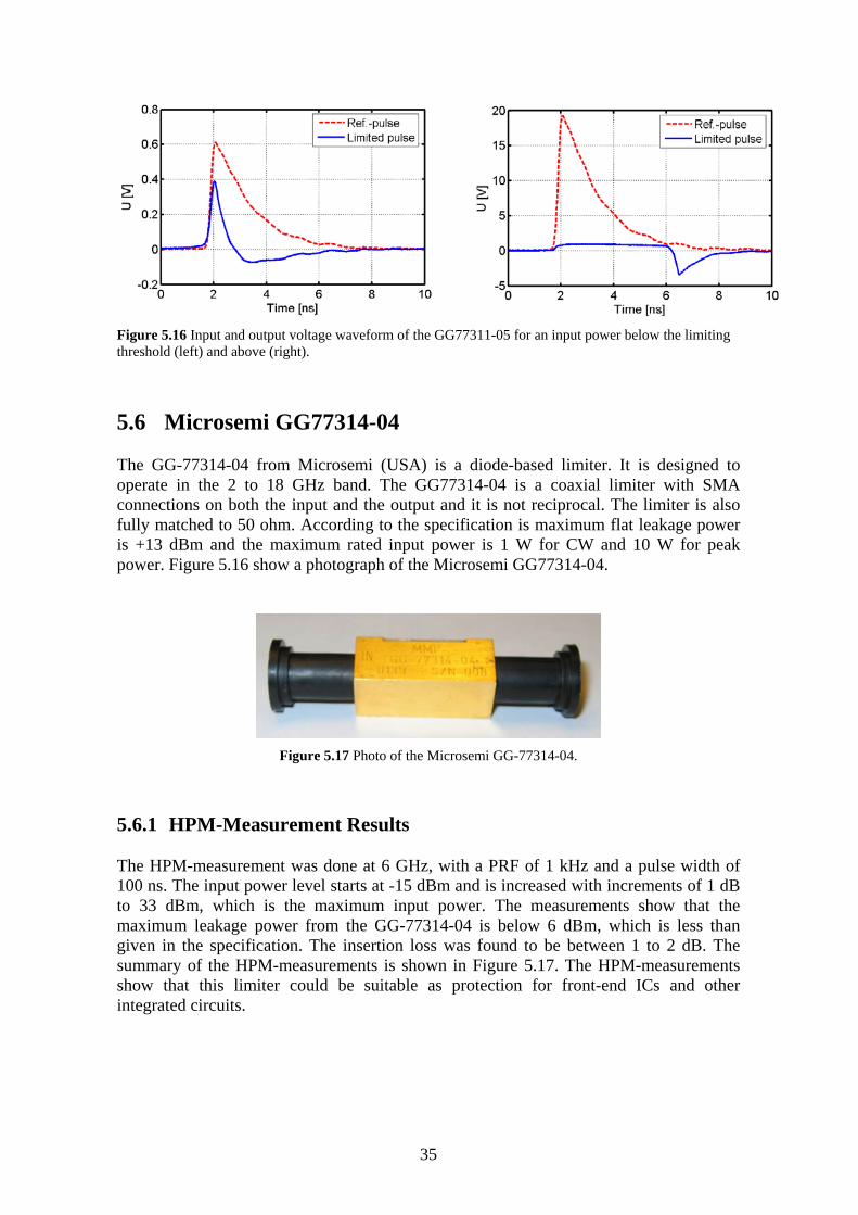
Figure 5.16 Input and output voltage waveform of the GG77311-05 for an input power below the limiting threshold (left) and above (right).
5.6 Microsemi GG77314-04 The GG-77314-04 from Microsemi (USA) is a diode-based limiter. It is designed to operate in the 2 to 18 GHz band. The GG77314-04 is a coaxial limiter with SMA connections on both the input and the output and it is not reciprocal. The limiter is also fully matched to 50 ohm. According to the specification is maximum flat leakage power is +13 dBm and the maximum rated input power is 1 W for CW and 10 W for peak power. Figure 5.16 show a photograph of the Microsemi GG77314-04.
Figure 5.17 Photo of the Microsemi GG-77314-04.
5.6.1 HPM-Measurement Results The HPM-measurement was done at 6 GHz, with a PRF of 1 kHz and a pulse width of 100 ns. The input power level starts at -15 dBm and is increased with increments of 1 dB to 33 dBm, which is the maximum input power. The measurements show that the maximum leakage power from the GG-77314-04 is below 6 dBm, which is less than given in the specification. The insertion loss was found to be between 1 to 2 dB. The summary of the HPM-measurements is shown in Figure 5.17. The HPM-measurements show that this limiter could be suitable as protection for front-end ICs and other integrated circuits.
35
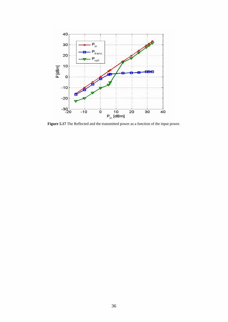
Figure 5.17 The Reflected and the transmitted power as a function of the input power.
36
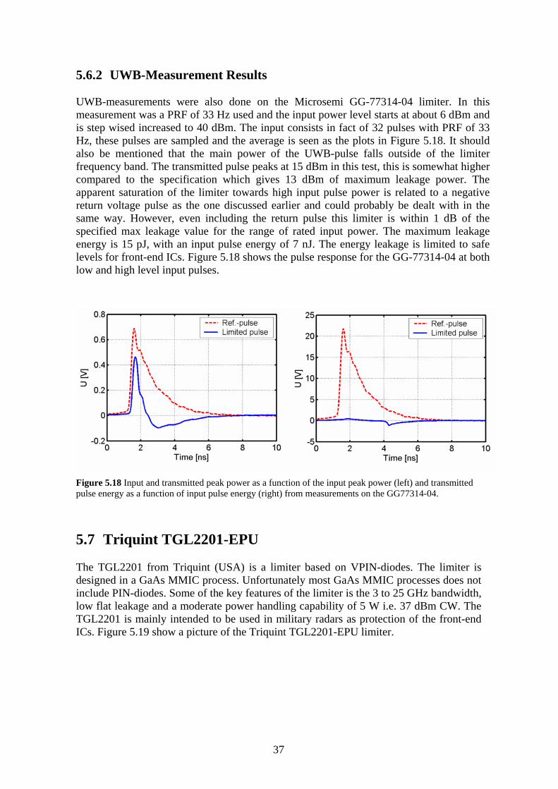
5.6.2 UWB-Measurement Results UWB-measurements were also done on the Microsemi GG-77314-04 limiter. In this measurement was a PRF of 33 Hz used and the input power level starts at about 6 dBm and is step wised increased to 40 dBm. The input consists in fact of 32 pulses with PRF of 33 Hz, these pulses are sampled and the average is seen as the plots in Figure 5.18. It should also be mentioned that the main power of the UWB-pulse falls outside of the limiter frequency band. The transmitted pulse peaks at 15 dBm in this test, this is somewhat higher compared to the specification which gives 13 dBm of maximum leakage power. The apparent saturation of the limiter towards high input pulse power is related to a negative return voltage pulse as the one discussed earlier and could probably be dealt with in the same way. However, even including the return pulse this limiter is within 1 dB of the specified max leakage value for the range of rated input power. The maximum leakage energy is 15 pJ, with an input pulse energy of 7 nJ. The energy leakage is limited to safe levels for front-end ICs. Figure 5.18 shows the pulse response for the GG-77314-04 at both low and high level input pulses.
Figure 5.18 Input and transmitted peak power as a function of the input peak power (left) and transmitted pulse energy as a function of input pulse energy (right) from measurements on the GG77314-04.
5.7 Triquint TGL2201-EPU The TGL2201 from Triquint (USA) is a limiter based on VPIN-diodes. The limiter is designed in a GaAs MMIC process. Unfortunately most GaAs MMIC processes does not include PIN-diodes. Some of the key features of the limiter is the 3 to 25 GHz bandwidth, low flat leakage and a moderate power handling capability of 5 W i.e. 37 dBm CW. The TGL2201 is mainly intended to be used in military radars as protection of the front-end ICs. Figure 5.19 show a picture of the Triquint TGL2201-EPU limiter.
37
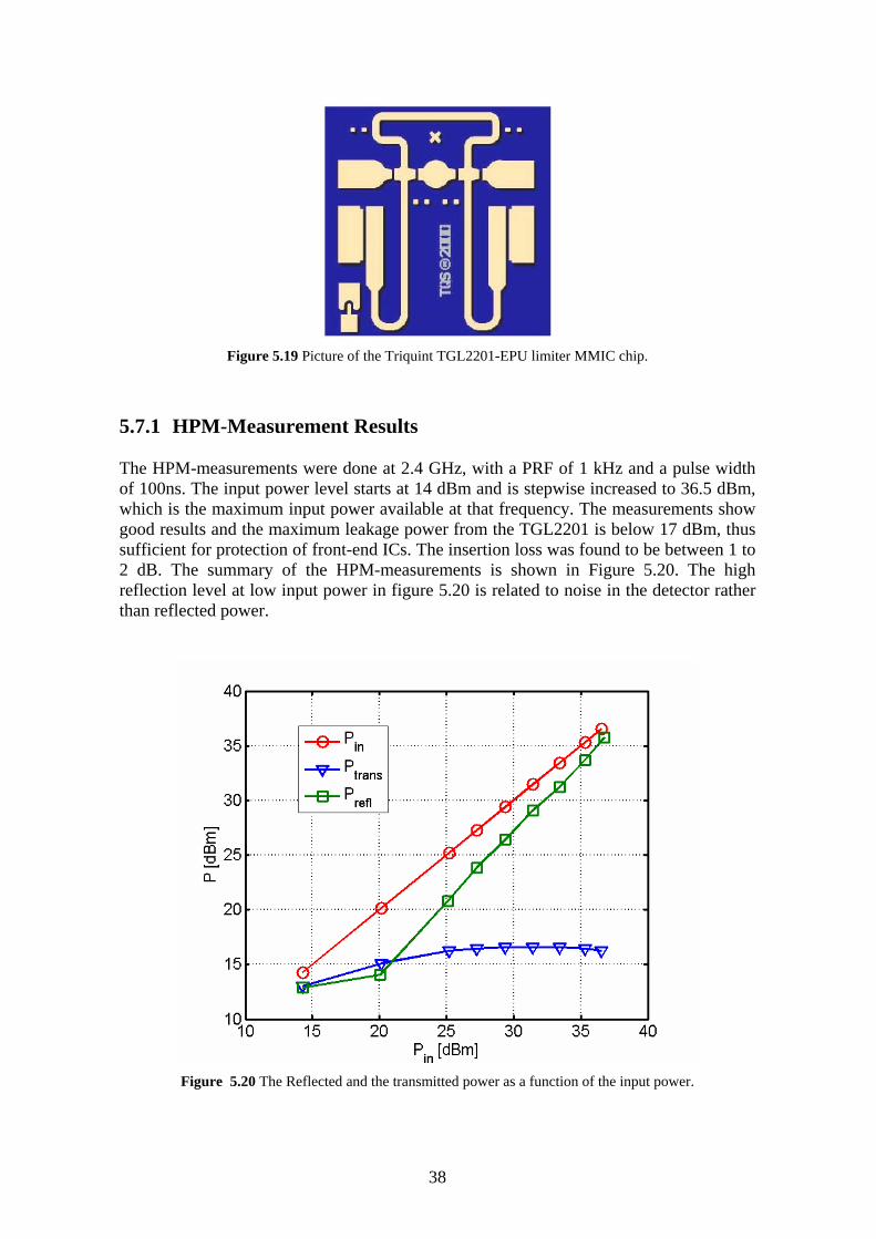
Figure 5.19 Picture of the Triquint TGL2201-EPU limiter MMIC chip.
5.7.1 HPM-Measurement Results The HPM-measurements were done at 2.4 GHz, with a PRF of 1 kHz and a pulse width of 100ns. The input power level starts at 14 dBm and is stepwise increased to 36.5 dBm, which is the maximum input power available at that frequency. The measurements show good results and the maximum leakage power from the TGL2201 is below 17 dBm, thus sufficient for protection of front-end ICs. The insertion loss was found to be between 1 to 2 dB. The summary of the HPM-measurements is shown in Figure 5.20. The high reflection level at low input power in figure 5.20 is related to noise in the detector rather than reflected power.
Figure 5.20 The Reflected and the transmitted power as a function of the input power.
38
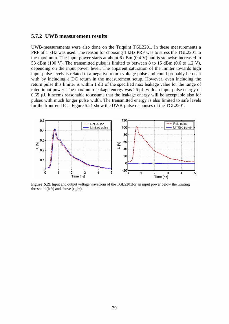
5.7.2 UWB measurement results UWB-measurements were also done on the Triquint TGL2201. In these measurements a PRF of 1 kHz was used. The reason for choosing 1 kHz PRF was to stress the TGL2201 to the maximum. The input power starts at about 6 dBm (0.4 V) and is stepwise increased to 53 dBm (100 V). The transmitted pulse is limited to between 8 to 15 dBm (0.6 to 1.2 V), depending on the input power level. The apparent saturation of the limiter towards high input pulse levels is related to a negative return voltage pulse and could probably be dealt with by including a DC return in the measurement setup. However, even including the return pulse this limiter is within 1 dB of the specified max leakage value for the range of rated input power. The maximum leakage energy was 26 pJ, with an input pulse energy of 0.65 µJ. It seems reasonable to assume that the leakage energy will be acceptable also for pulses with much longer pulse width. The transmitted energy is also limited to safe levels for the front-end ICs. Figure 5.21 show the UWB-pulse responses of the TGL2201.
Figure 5.21 Input and output voltage waveform of the TGL2201for an input power below the limiting threshold (left) and above (right).
39

40
6 Summary and Conclusions An extensive investigation of front-door protection devices has been made. The investigation includes a survey of different technologies that potentially can be used for front-door protection. A survey of the HPM- and UWB-threats to electronic equipment is also provided in this thesis. The investigation also involves preparation and a lot hands-on management of several measurement equipments, like different amplifiers, power-meters, oscilloscopes etc. The measurements have resulted in interesting results. Several conclusions can be drawn from the measurement results. The results show that some of the tested devices are not suitable as front-door protection against HPM- and UWB-pulses. Other devices have showed to provide quit good protection against both HPM- and UWB-pulses. The diode-based limiters have in general showed a good capability to protect from both HPM- and UWB-pulses. They are in fast acting devices with short response- and recovery-time. They are also able to withstand moderate CW and peak pulse power/energy levels. Further they also introduce relatively small insertion loss and they are able to work for broad frequency bands, up to tens of GHz. The diode limiters are also small in size, which makes them to an attractive alternative for integration with array antennas and other applications where the size is critical. However if the power/energy levels are higher, the diode limiters might suffer burnout, due to their lack of high power/energy handling capabilities. In this case other types of protection devices are required, which can handle higher power/energy levels. The Gas discharge tubes (GDTs) and the metal oxide varistors (MOVs) are protection devices which have better power/energy handling capabilities. The measurements of these devices have however showed rather poor results. The results from the GDT and the MOV showed only a small response to the input pulses, but they might have been triggered if the input power levels were higher, this will be further investigated. A combination of different technologies integrated into one limiter, i.e. a hybrid-circuit would be ideal. The combination of two different technologies, where the first stage takes care of high power/energy pulses and were a second stage the cleans up the remaining power/energy and the fast transients of the pulses. For high frequency limiters it is also important to have a low capacitance in order to minimize the insertion loss and noise figure, otherwise the overall system performance will be seriously degraded. This thesis work has given me deeper knowledge of different front-door protection technologies. It has also increased my skills in microwave measurements and handling of measurement equipment.
41

42
7 Future Work The future work that will follow this thesis work, consists in further investigation of limiters. The susceptibility of front-end receiver electronics will also be investigated, especially the LNA (Low Noise Amplifier), which in many systems is the first component to be exposed for UWB- and HPM-pulses. Further development of GaAs MMIC limiters at FOI will also be done. The main-part of the FOI front-end components is designed using GaAs MMIC processes. It is highly desirable to integrate both limiter and LNA on the same chip. A combination of Limiter and LNA would save both chip area and costs. The possibility to integrate the successfully tested limiters with common front-end electronics will be further investigated. The combination of limiter and LNA is interesting and could be of use in both civil and military electronic equipment.
43

44
8 Acknowledgements This thesis work was done at FOI in Linköping, where I also got help and support from many people. I would like to give special thank to Rolf Jonsson (FOI), Olof Lundén (FOI) and Dr. Mats Bäckström (Saab Communication) for helping me with this thesis work and for providing helpful information and valuable discussions. It should also be mentioned that parts of this thesis work also has been published in a FOI-report [24].
45

46
9 References and Literature [1] Daher K. J., (2005), EMC/EMI for Engineers and Engineering Managers, Georgia
Tech Research Institute, Georgia Institute of Technology, Sensor and Electromagnetic Applications Laboratory, Atlanta, Georgia 30332-0852
[2] Giri D. V., (2005), HIGH-POWER ELECTROMAGNETIC (HPEM) RADIATORS and INTENTIONAL ELECTROMAGNETIC INTERFERENCE (IEMI), Plenary Talk at RVK 2005, Radio Vetenskap och Kommunikation. Linköping, Sweden
[3] Andersson P., (2000), Skydd mot framvägskoppling, Swedish Defence Research
Agency FOI, P.O. Box 1165, SE-581 11 Linköping, Sweden, FOA Memo 00-5647/L.
[4] Benford J. and Swegle J., (1992), High-Power Microwaves, Artech House Books,
USA, ISBN: 0-89006-415-6
[5] SRC Devices, Surge Arrester Technologies, Application Note AN-111 http://www.srcdevices.com/pdf/an111_r1.pdf(Acc 2006-10-12)
[6] CPI Beverly Microwave Division, (2002). Receiver Protector Technology,
http://www2.cpii.com/bmd/rptech1.htm. (Acc. 2006-10-12)
[7] Weston. D. A., (2000), Electromagnetic Compatibility, Dekker, USA, ISBN: 0-8247-8889-3
[8] Zitink M., (1999) Transient protection of electrical systems: Development of
design tools, Uppsala University, UURIE 281-99 L, ISSN 0349-8352 [9] Walters K., Clark M., (2002), An Introduction to Transient Voltage Suppressor
Devices http://www.microsemi.com/micnotes/102.pdf. (Acc. 2006-10-12) [10] Jordan U., Private communication, Chalmers University of Technology,
Department of Electromagnetics, SE-412 96 Göteborg, Telephone: +46 31 772 1569, Fax: +46 31 772 1573, E-mail: [email protected]
[11] Bäckström M., et al, (2001), HPM. Framvägskoppling och skydd. Lägesrapport,
Swedish Defence Research Agency FOI, P.O. Box 1165, SE-581 11 Linköping, Sweden, FOI-R--0265--SE, ISSN 1650-1942.
[12] Andersson D. et al, Microwave Breakdown in Slots, Proceedings from RVK 02,
Stockholm, June 10-13 2002, Pages 291- 294. [13] Harris Suppression Products / Littlefuse, (January 1998), Transient Suppression
Devices and Principles, Application Note AN9768, http://www.littelfuse.com/data/en/Application_Notes/an9768.pdf, (Acc. 2006-10-12)
47
[14] Streetman G. B., Banerjee S., (2000), Solid State Electronic Devices, Fifth edition, ISBN: 0-13-025538-6
[15] Prasad Kodali V., (1996), Engineering Electromagnetic Compatibility:
Principles, Measurements, and Technologies, IEEE Publications, ISBN: 0-7803-1117-5.
[16] Jonsson R., Nilsson T. and Bäckström M., (2005), Design and Characterization of Limiters for HPM Front Door Protection, RVK 2005, proceedings pp xx-y, Linköping, Sweden [17] Tyco / electronics M/A-COM Datasheet, X-Band Limiter/Low Noise Amplifier
8.5 –12.0 GHz, RS-O-P-DS-3003, Customer Service Europe: Tel. +44 (1344) 869 595, Fax+44 (1344) 300 020, URL: www.macom.com
[18] TriQuint Semiconductor, (2003), Wideband Dual Stage VPIN Limiter TGL2201-
EPU, TGL2201-EPU, TriQuint Semiconductor Texas (USA): Phone (972)994-8465 Fax (972)994 8504, URL: www.triquint.com
[19] Hiller G., MA-COM, (200?), Application Note, AG312, Designing with PIN-
diodes,http://www.macom.com/Application%20Notes/pdf/ag312.pdf#search=%22AG312%22 , V2.00, (Acc 2006-10-12)
[20] Balevicius S., PUFETs Semiconductor protectors against EMP, (1995?), PFI
Semiconductor Physics Institute, Vilnius, Lithuania. [21] Whitaker J. C. (redactor), (1996), chapter Transient Suppression Components in,
The Electronics Handbook, CRC Press, Oregon USA, ISBN: 0-8493-8345-5. [22] Walters K., Clark M., (2002). What is a Thyristor Surge Protector Device,
http://www.microsemi.com/micnotes/105.pdf (Acc. 2006-10-12) [23] Lundén O., (December 1999), Användarhandledning för
Mikrovågsinjiceringsmätsystem för Elektronikkomponenter (MIMEC), Version 1.0, Swedish Defence Research Agency FOI, P.O. Box 1165, SE-581 11 Linköping, Sweden, FOA-D—99-00459-612—SE.
[24] Nilsson T. and Jonsson R., (2005), Investigation of HPM Front-door Protection
Devices and Component Susceptibility, Swedish Defence Research Agency FOI, P.O. Box 1165, SE-581 11 Linköping, Sweden, FOI-R--1772--SE, ISSN 1650-1942.
48
På svenska Detta dokument hålls tillgängligt på Internet – eller dess framtida ersättare – under en längre tid från publiceringsdatum under förutsättning att inga extra-ordinära omständigheter uppstår.
Tillgång till dokumentet innebär tillstånd för var och en att läsa, ladda ner, skriva ut enstaka kopior för enskilt bruk och att använda det oförändrat för ickekommersiell forskning och för undervisning. Överföring av upphovsrätten vid en senare tidpunkt kan inte upphäva detta tillstånd. All annan användning av dokumentet kräver upphovsmannens medgivande. För att garantera äktheten, säkerheten och tillgängligheten finns det lösningar av teknisk och administrativ art.
Upphovsmannens ideella rätt innefattar rätt att bli nämnd som upphovsman i den omfattning som god sed kräver vid användning av dokumentet på ovan beskrivna sätt samt skydd mot att dokumentet ändras eller presenteras i sådan form eller i sådant sammanhang som är kränkande för upphovsmannens litterära eller konstnärliga anseende eller egenart.
För ytterligare information om Linköping University Electronic Press se förlagets hemsida http://www.ep.liu.se/ In English The publishers will keep this document online on the Internet - or its possible replacement - for a considerable time from the date of publication barring exceptional circumstances.
The online availability of the document implies a permanent permission for anyone to read, to download, to print out single copies for your own use and to use it unchanged for any non-commercial research and educational purpose. Subsequent transfers of copyright cannot revoke this permission. All other uses of the document are conditional on the consent of the copyright owner. The publisher has taken technical and administrative measures to assure authenticity, security and accessibility.
According to intellectual property law the author has the right to be mentioned when his/her work is accessed as described above and to be protected against infringement.
For additional information about the Linköping University Electronic Press and its procedures for publication and for assurance of document integrity, please refer to its WWW home page: http://www.ep.liu.se/ © Tony Nilsson


![HPM [1]BOLT](https://img.pdfslide.us/doc/110x75/5480023f5906b5ea288b46ae/hpm-1bolt.jpg)