Embed Size (px)
Citation preview
General rights Copyright and moral rights for the publications made accessible in the public portal are retained by the authors and/or other copyright owners and it is a condition of accessing publications that users recognise and abide by the legal requirements associated with these rights.
• Users may download and print one copy of any publication from the public portal for the purpose of private study or research. • You may not further distribute the material or use it for any profit-making activity or commercial gain • You may freely distribute the URL identifying the publication in the public portal
If you believe that this document breaches copyright please contact us providing details, and we will remove access to the work immediately and investigate your claim.
Downloaded from orbit.dtu.dk on: Jul 03, 2018
Investigation of DC magnetron-sputtered TiO2 coatings: Effect of coating thickness,structure, and morphology on photocatalytic activity
Daviðsdóttir, Svava; Shabadi, Rajashekhara; Galca, Aurelian Catalin ; Hald Andersen, Inge ; Dirscherl,Kai; Ambat, RajanPublished in:Applied Surface Science
Link to article, DOI:10.1016/j.apsusc.2014.06.047
Publication date:2014
Link back to DTU Orbit
Citation (APA):Daviðsdóttir, S., Shabadi, R., Galca, A. C., Hald Andersen, I., Dirscherl, K., & Ambat, R. (2014). Investigation ofDC magnetron-sputtered TiO2 coatings: Effect of coating thickness, structure, and morphology on photocatalyticactivity. Applied Surface Science, 313, 677–686. DOI: 10.1016/j.apsusc.2014.06.047
Accepted Manuscript
Title: Investigation of DC magnetron-sputtered TiO2 coatings:Effect of coating thickness, structure, and morphology onphotocatalytic activity
Author: Svava Daviðsdottir Rajashekhara Shabadi AurelianCatalin Galca Inge Hald Andersen Kai Dirscherl Rajan Ambat
PII: S0169-4332(14)01318-XDOI: http://dx.doi.org/doi:10.1016/j.apsusc.2014.06.047Reference: APSUSC 28096
To appear in: APSUSC
Received date: 1-4-2014Revised date: 6-6-2014Accepted date: 8-6-2014
Please cite this article as: S. Daviethsdottir, R. Shabadi, A.C. Galca, I.H. Andersen, K.Dirscherl, R. Ambat, Investigation of DC magnetron-sputtered TiO2 coatings: Effect ofcoating thickness, structure, and morphology on photocatalytic activity, Applied SurfaceScience (2014), http://dx.doi.org/10.1016/j.apsusc.2014.06.047
This is a PDF file of an unedited manuscript that has been accepted for publication.As a service to our customers we are providing this early version of the manuscript.The manuscript will undergo copyediting, typesetting, and review of the resulting proofbefore it is published in its final form. Please note that during the production processerrors may be discovered which could affect the content, and all legal disclaimers thatapply to the journal pertain.
Page 1 of 26
Accep
ted
Man
uscr
ipt
1
Investigation of DC magnetron-sputtered TiO2 coatings: Effect of coating thickness, structure, and morphology on photocatalytic activity
Svava Daviðsdóttir*a, Rajashekhara Shabadib, Aurelian Catalin Galcac, Inge Hald Andersend,Kai Dirscherle, and Rajan Ambata,
a Division of Materials and Surface and Engineering, Department of Mechanical Engineering, Technical University of Denmark, DK-2800 Kgs. Lyngby, Denmark
bDenmark d Unité Matériaux et Transformations, C6, Université Lille, 59655 Villeneuve ‘Ascq, France
cLaboratory of Multifunctional Materials and Structures, National Institute of Materials Physics, RO-077125, Măgurele-Bucharest, Romania
dDanish Technological Institute, Tribology Centre, Teknologiparken, Building 18, Kongsvang All 29, DK-8000 Aarhus C, Denmark
eDanish Fundamental Metrology, Matematiktorvet 307, DK-2800 Kgs. Lyngby, Denmark
Keywords: photocatalysis, TiO2, coatings, magnetron-sputtering, electrochemical impedance spectroscopy
Abstract The photocatalytic performance of magnetron-sputtered titanium dioxide (TiO2) coatings of
different thickness in anatase crystalline structure deposited on aluminium 1050 alloy
substrates was investigated using a combination of photo-electrochemistry, methylene blue
decomposition, and microscopic and spectroscopic methods, such as high resolution scanning
and transmission electron microscopy, atomic force microscopy and ellipsometry. The
reaction resistance was measured by AC impedance, while photocurrent measurements were
carried out using the zero resistance ammetry (ZRA) method. The results showed that the
TiO2 grains grow in dipyramidal columns having a linear increase in surface area with
increased coating thickness. The refractive index values indicate also an evolutionary growth.
The refractive index values obtained for the thin coatings on aluminium substrate were well
below the values reported for monocrystalline anatase. The photocatalytic performance
Page 2 of 26
Accep
ted
Man
uscr
ipt
2
increased with increased coating thickness, though more rapidly over a range of 100 - 500 nm
thickness. The dielectric constant also increased linearly with coating thickness
1 IntroductionThere is growing interest in titanium dioxide (TiO2) in the anatase crystalline form due to the
usefulness of its photocatalytic activity for number applications. These include solar energy
conversion[1],[2] electro-chromic devices[3], photocatalytic applications in air and water
purification[4], self-cleaning and antimicrobial surfaces[5]. Therefore, significant research is
being undertaken all over the world to understand the relationship between photocatalysis and
morphology of TiO2 as a means to enhance its performance[6],[7],[8],[9].
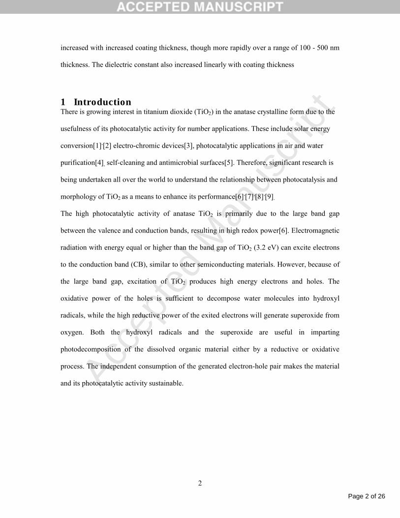
The high photocatalytic activity of anatase TiO2 is primarily due to the large band gap
between the valence and conduction bands, resulting in high redox power[6]. Electromagnetic
radiation with energy equal or higher than the band gap of TiO2 (3.2 eV) can excite electrons
to the conduction band (CB), similar to other semiconducting materials. However, because of
the large band gap, excitation of TiO2 produces high energy electrons and holes. The
oxidative power of the holes is sufficient to decompose water molecules into hydroxyl
radicals, while the high reductive power of the exited electrons will generate superoxide from
oxygen. Both the hydroxyl radicals and the superoxide are useful in imparting
photodecomposition of the dissolved organic material either by a reductive or oxidative
process. The independent consumption of the generated electron-hole pair makes the material
and its photocatalytic activity sustainable.
Page 3 of 26
Accep
ted
Man
uscr
ipt
3
Figure 1. A schematic showing the TiO2 photocatalytic process. The UV-light absorbed will generate an electron-hole pair in the valence and conduction band respectively.
The photocatalytic activity of TiO2 is influenced by a number of parameters, including the
morphology of the TiO2 particles or coatings, processing methods, crystallographic
orientation, and the presence of dopants. It has been reported that the 004 face of TiO2, due to
constrained alignment of the surface atoms[10], is more active than the 101 face
[11],[12],[10]. A number of investigations have demonstrated that larger surface area
increases the photocatalytic activity, and the photocatalytic activity was improved by addition
of various dopants such as Cr, Mo, V, Mn, Fe, Co and Ni[13],[14].
Most investigations in the literature related to photocatalysis of TiO2 focused on nano-
particles and coatings on glass substrates. A review by Debold[15] is a good summary of
research done on TiO2 and shows the increased interest in this area as reflected by the
increased number of publications, especially on single-crystalline TiO2. Moreover, this paper
gives a brief introduction on metal/titanium dioxide interfaces and highlights its relevancy for
further studies. It has been reported that the behaviour of TiO2 coatings on a metallic substrate
is different from that of a non-metallic substrate due to the interplay between the conduction
band of the substrate metal, band structure of the interfacing oxide, and band structure of
Page 4 of 26
Accep
ted
Man
uscr
ipt
4
TiO2[16]. Previous studies of TiO2 coatings on metallic substrates have demonstrated that the
substrate can assist the charge separation and electron transfer, and increased coating
thickness increases the activation depth and UV-absorption until a saturation depth of the
coating is reached [17].
The change in coating thickness can influence the morphology and surface area of the top
layer of the coating, which will have significant impact on the photocatalytic performance.
The surface morphology of TiO2 also depends on the synthesis method. There are various
techniques for synthesizing TiO2 coatings[3]. Among, and the most common methods are
chemical solution deposition (CSD, Sol gel)[18],[19] and physical vapour deposition
(PVD)[20],[21]. PVD is known to produce compact coatings with good adhesion to the
substrate and the processing parameters, such as temperature and pressure, are controlled
precisely and hence provide good reproducibility.
When a coating is deposited by vacuum techniques such as PVD, the size of the crystallites
can increases with increased coating thickness due to the evolutionary nature of the
growth[22]. In larger crystallites, the lifetime of the electron/hole is also lengthened as the
pair migrates a greater distance in large crystallites than in smaller crystallites[23]. Greater
electron-hole recombination distance increases the photocurrent, allowing more photocatalytic
decompositions to take place.
The investigation reported in this paper focuses on the magnetron-sputtered TiO2 coatings of
different thicknesses on an aluminium alloy (AA1050) substrate. Microstructural and surface
morphological investigations were performed by atomic force microscopy (AFM), scanning
electron microscopy (SEM), transmission electron microscopy (TEM), x-ray diffraction
(XRD), and glow discharge optical emission spectroscopy (GDOES). The photocatalytic
activity was determined by measuring:: (i) the reaction resistance under UV illumination
based on impedance measurements, (ii) photocurrent upon UV illumination using zero
Page 5 of 26
Accep
ted
Man
uscr
ipt
5
resistance ammetry (ZRA), and (iii) the photocatalytic decomposition of methylene blue on
TiO2 surfaces using UV light.
2 Material and methods
Substrate preparation: The substrate material used for the present investigation was AA1050
aluminium. AA1050 has a chemical composition (in %) of Cu (0–0.05), Mg (0–0.05), Si (0–
0.25), Fe (0–0.4), Mn (0–0.05), Zn (0–0.07), Ti (0–0.07) and Al (balance). All the coated
specimens were of the size 5cm x 5cm. The surface was polished to 1 micron surface finish
by using a buffing machine (Polette 6NE from KE MOTOR A/S).
TiO2 coating Synthesis: The TiO2 coating on aluminium substrates was carried out by pulsed
DC magnetron sputtering using an industrial CemeCon CC800/9 SinOx coating unit. The
sputtering chamber was equipped with four magnetrons, each mounted with a 500mm x
88mm Ti target (purity 99.5 wt.%). A pulsed DC power of 2 kW was applied to each
magnetron, where the cathodes are running in dual magnetron sputtering mode at a frequency
of 50Hz. The depositions were carried out in an argon/oxygen atmosphere at a total pressure
of about 400 mPa. The Ar/O2 gas flow ratio was 350 sccm/150 sccm, resulting in
stoichiometric TiO2 coatings. The deposition temperature was approximately 150 °C, and it
was controlled by a resistive heater. The substrate was at floating potential where the self-bias
was between -6V and -9V. The deposition rate was 2.4 nm/min. The TiO2 coatings used for
the present investigation were approximately 100 nm, 500 nm, and 2 µm thick.
Microstructural characterisation: Surface morphology and microstructural characterization of
the coatings were carried out using FEG-SEM (SEM Quanta 200f). A Tecnai T-20 machine
operating at 200 kV was used to study the FIB cuts from the depths of the coating thickness.
The surface topography was studied using AFM in tapping mode (Dimension3100
Metrology). Chemical depth profiling of the coating was carried out using GDOES (RF
GDOES GD profiler 2).
X-Ray diffraction: Phase analysis of the coating was examined with X-ray diffractometer
(XRD) (D8 Discover). The measurement was carried out in grazing incident mode with an
incident angle of 0.7°.
Page 6 of 26
Accep
ted
Man
uscr
ipt
6
Refractive index and high-frequency dielectrical constant: Optical measurements were
performed with a Woollam Variable Angle Spectroscopic Ellipsometer, equipped with a high
pressure Xenon discharge lamp incorporated in an HS-190 monochromator. Measurements
were done in the IR-Vis-UV region of the spectrum at photon energies between 0.7 (~1771
nm) and 6.2 eV (248 nm), step of 0.01 eV, and at 45, 60 and 75º angles of incidence.
Tests using methylene blue decomposition: Decomposition of methylene blue by
photocatalytic TiO2 surface was used for measuring the photocatalytic activity (redox
indicator) of the surface according to the DIN standard 52980 entitled “Photocatalytic activity
of surfaces –Determination of photocatalytic activity by degradation of methylene blue”[24].
The experiment was conducted using a flow cell in which the solution was exposed to TiO2
surface (area of 11 cm2) under UV light (with intensity of 2.9 mW for photon energy of 3.2
eV, or 0.26 mW/cm2), and the reacted solution was analysed for a decrease in methylene blue
concentration using a UV spectrophotometer. A reference experiment was carried out just
with aluminium substrate in order to determine the amount of methylene blue decomposed
just by the UV light without TiO2 surface. Prior to the testing, all the samples were pre-soaked
in the MB solution for 2 hours and the MB solution was then exchanged for fresh solution
before testing.
Photo-electrochemical testing: Electrochemical measurements were used to understand the
photocatalytic behaviour of TiO2 surface with and without UV light exposure. A standard
three electrode electrochemical cell set up was used for these measurements. The
electrochemical cell consisted of a quartz window and the specimen was loaded on the other
side of the cell facing the quartz window. The specimen was pressed against an O-ring
exposing a surface area of 9.6 cm2 to the solution. The quartz window was used to expose the
specimen to the UV light by placing a UV source facing the quartz window. The reference
electrode used for the measurement was Hg/Hg2SO4/saturated K2SO4 in order to avoid any
chloride contamination to the solution. The counter electrode used was platinum. The
electrolyte used for all experiments was de-ionized water with analytic grade 0.1 M NaNO3
for increasing the conductivity of the solution. The volume of the electrolyte used was 550 ml.
The UV lamp used was a Philips home solarium and it was placed at 35 cm distance from
sample. The (ZRA) technique was used for measuring the current response between the
sample and a platinum electrode with and without UV. The increase in current under UV
Page 7 of 26
Accep
ted
Man
uscr
ipt
7
exposure represents the photocurrent due to photocatalysis. The potentiostat used for the
experiments was Gill AC BI-STAT.
Electrochemical impedance measurements: Electrochemical impedance measurements were
used to analyse the charge-transfer characteristics of the TiO2 coated sample across the
coating. The transport of charge between the coating and substrate depends on the activation
depth of the anatase coating, and any interface oxide layer present on the substrate surface.
The impedance measurements were performed from 1 Hz to 1000 Hz with potentials ranging
from -0.4 to +0.74. The potentiostat used for the experiments was VSP from Bio Logic.
3 Results and Discussion
3.1 Effect of coating thickness on anatase crystallite size and interface
microstructure
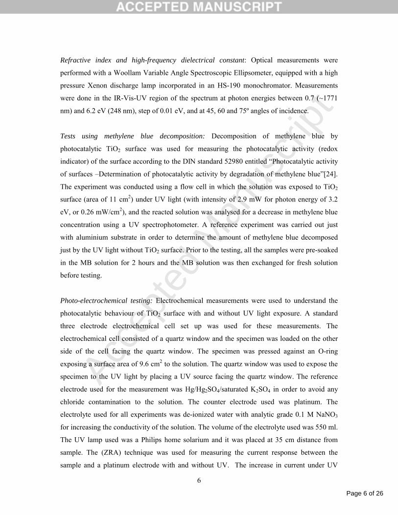
3.1.1 Glow discharge optical emission spectroscopyFigure 2 shows the chemical depth profile of the TiO2 coating of different thicknesses on
aluminium 1050 substrate prepared by pulsed DC magnetron sputtering. The deposition rate
was 2.4 nm/min and the thickness was assumed to increase linearly as a function of the
deposition time. From the calibrated GDOES profile, the thicknesses were estimated to be
around 100 nm, 500 nm, and 2 µm. Compositional depth profiles of the Ti/O ratio indicated
that the coating is stoichiometrically correct, with approximately 33 atomic % at Ti and 66
atomic % at O.
0 50 1000
20
40
60
80
100
sputtering time [s]
Ratio in ato
mic %
0 50 1000
20
40
60
80
100
sputtering time [s]
Ratio in atomic %
0 50 1000
20
40
60
80
100
sputtering time [s]
Ratio in atomic %
AlTiO
Figure 2. GDOES compositional depth profile of the TiO2 coating thickness in at % of a) 100 nm, b) 500 nm, c) 2 µm.
ba c
Page 8 of 26
Accep
ted
Man
uscr
ipt
8
All the profiles showed enhanced oxygen concentration near the surface, which is assumed to
be due to trapped oxygen in the top layers of the rough (nano-scale) surface.
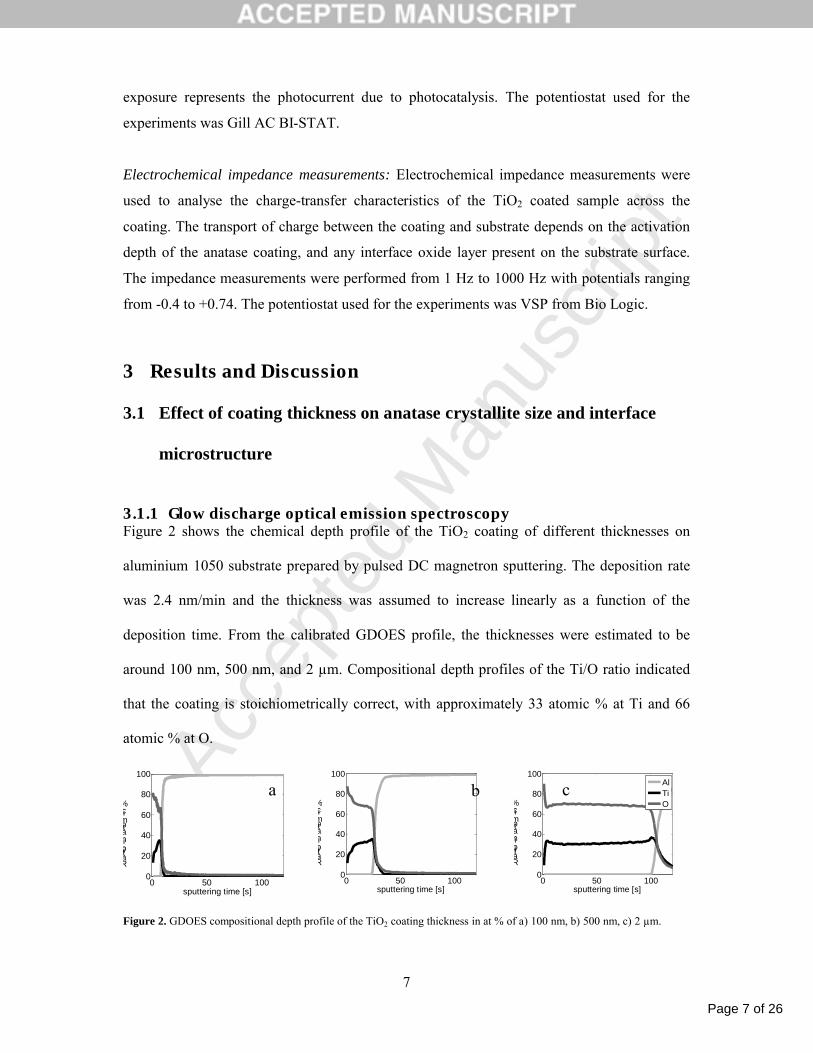
2.1.2 Scanning electron microscopy
Figure 3 a-c shows top view SEM images of the TiO2 coatings with increased thickness, from
100 nm, 500 nm, and 2000 nm, respectively, on aluminium. The SEM images clearly show
that the TiO2 crystals grow in dipyramidal columns. As the coating thickness increases, the
columns become wider with an increase in lateral column sizes.
Figure 3. SEM images of the top view of TiO2 coating thickness of: a) 100 nm, b) 500 nm and c) 2 µm.
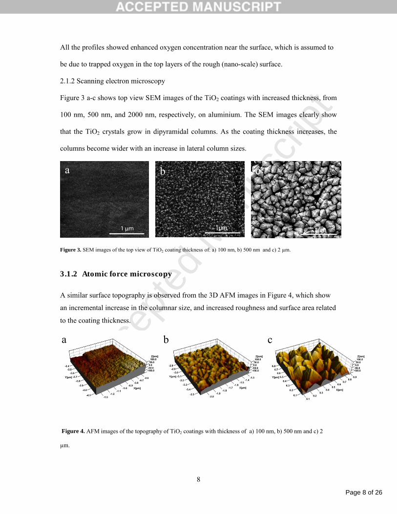
3.1.2 Atomic force microscopy
A similar surface topography is observed from the 3D AFM images in Figure 4, which show
an incremental increase in the columnar size, and increased roughness and surface area related
to the coating thickness.
Figure 4. AFM images of the topography of TiO2 coatings with thickness of a) 100 nm, b) 500 nm and c) 2
µm.
a b c
a b c
Page 9 of 26
Accep
ted
Man
uscr
ipt
9
Quantitative measurements of the AFM images reveal that there is a linear relationship
between the thicknesses of the coating and widening of the columns which define the in-plane
cross-sectional area of the columns (Figure 5). As the width of the column increases, the
surface area also increases. The plot in Figure 5b shows that the surface area increases
linearly with thickness of the coating due to increased roughness. The surface area ratio was
calculated with the commercial software “Scanning Probe Image Processor SPIP” (Image
Metrology A/S, Hoersholm, Denmark) according to the standard ISO/DIS 25178-2, where the
percentage increase in the interfacial surface area relative to the projected area is calculated.
The increased surface area is advantageous for photocatalytic activity as it provides more sites
for the reactions to occur[6],[25].
0 500 1000 1500 2000-0.5
0
0.5
1
1.5
2
2.5x 10
4
film thickness [nm]cross-sectional area of the colu
mn [n
m2]
0 500 1000 1500 2000 25000
50
100
150
200
film thickness [nm]
surface area ratio[%]
Figure 5: Sputter coated TiO2 coating: a) Correlation between coating thickness and column in-plane cross
section area. b) Correlation between coating thickness and surface area ratio
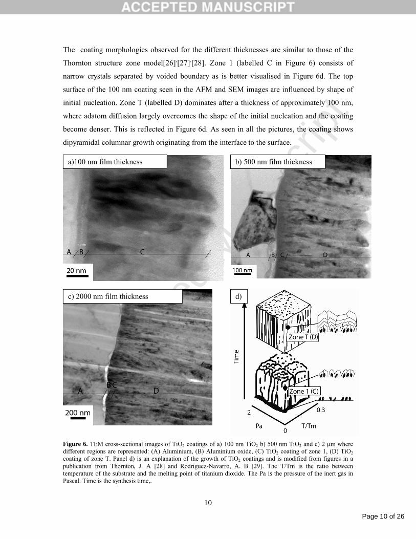
3.1.3 Transmission electron microscopy
The TEM image presented in Figure 6 shows the cross-sectional profile of coatings of various
thicknesses. The magnified image for the 100 nm thickness (Figure 6a) shows that
approximately 4 nm of aluminium oxide layer is present. Furthermore, Figure 6b shows that
the coating texture consists of two different zones, labelled C and D in the figure. The
formation of the zones is influenced by the processing parameters; the pressure is 4 mPa and
the ratio between the surface temperature and the melting point of the coating is below 0.3.
a) b)
Page 10 of 26
Accep
ted
Man
uscr
ipt
10
The coating morphologies observed for the different thicknesses are similar to those of the
Thornton structure zone model[26],[27],[28]. Zone 1 (labelled C in Figure 6) consists of
narrow crystals separated by voided boundary as is better visualised in Figure 6d. The top
surface of the 100 nm coating seen in the AFM and SEM images are influenced by shape of
initial nucleation. Zone T (labelled D) dominates after a thickness of approximately 100 nm,
where adatom diffusion largely overcomes the shape of the initial nucleation and the coating
become denser. This is reflected in Figure 6d. As seen in all the pictures, the coating shows
dipyramidal columnar growth originating from the interface to the surface.
Figure 6. TEM cross-sectional images of TiO2 coatings of a) 100 nm TiO2 b) 500 nm TiO2 and c) 2 µm where different regions are represented: (A) Aluminium, (B) Aluminium oxide, (C) TiO2 coating of zone 1, (D) TiO2
coating of zone T. Panel d) is an explanation of the growth of TiO2 coatings and is modified from figures in a publication from Thornton, J. A [28] and Rodriguez-Navarro, A. B [29]. The T/Tm is the ratio between temperature of the substrate and the melting point of titanium dioxide. The Pa is the pressure of the inert gas in Pascal. Time is the synthesis time,.
a)100 nm film thickness b) 500 nm film thickness
c) 2000 nm film thickness d)
Page 11 of 26
Accep
ted
Man
uscr
ipt
11
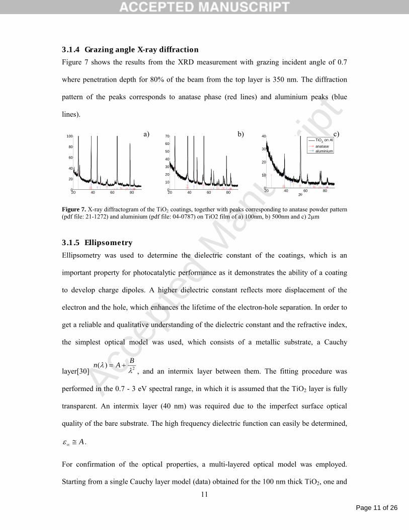
3.1.4 Grazing angle X-ray diffraction
Figure 7 shows the results from the XRD measurement with grazing incident angle of 0.7
where penetration depth for 80% of the beam from the top layer is 350 nm. The diffraction
pattern of the peaks corresponds to anatase phase (red lines) and aluminium peaks (blue
lines).
20 40 60 800
20
40
60
80
100
20 40 60 800
10
20
30
40
50
60
70
20 40 60 800
10
20
30
40
2
TiO2 on Al
anatasealuminium
Figure 7. X-ray diffractogram of the TiO2 coatings, together with peaks corresponding to anatase powder pattern (pdf file: 21-1272) and aluminium (pdf file: 04-0787) on TiO2 film of a) 100nm, b) 500nm and c) 2µm
3.1.5 Ellipsometry
Ellipsometry was used to determine the dielectric constant of the coatings, which is an
important property for photocatalytic performance as it demonstrates the ability of a coating
to develop charge dipoles. A higher dielectric constant reflects more displacement of the
electron and the hole, which enhances the lifetime of the electron-hole separation. In order to
get a reliable and qualitative understanding of the dielectric constant and the refractive index,
the simplest optical model was used, which consists of a metallic substrate, a Cauchy
layer[30] 2)(
BAn
, and an intermix layer between them. The fitting procedure was
performed in the 0.7 - 3 eV spectral range, in which it is assumed that the TiO2 layer is fully
transparent. An intermix layer (40 nm) was required due to the imperfect surface optical
quality of the bare substrate. The high frequency dielectric function can easily be determined,
A .
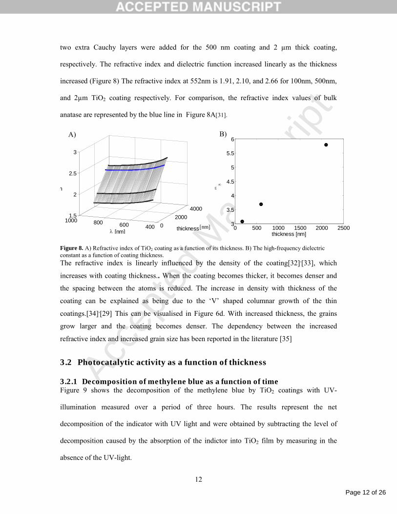
For confirmation of the optical properties, a multi-layered optical model was employed.
Starting from a single Cauchy layer model (data) obtained for the 100 nm thick TiO2, one and
a) b) c)
Page 12 of 26
Accep
ted
Man
uscr
ipt
12
two extra Cauchy layers were added for the 500 nm coating and 2 µm thick coating,
respectively. The refractive index and dielectric function increased linearly as the thickness
increased (Figure 8) The refractive index at 552nm is 1.91, 2.10, and 2.66 for 100nm, 500nm,
and 2µm TiO2 coating respectively. For comparison, the refractive index values of bulk
anatase are represented by the blue line in Figure 8A[31].
0
2000
4000
40060080010001.5
2
2.5
3
thickness [nm]
n
0 500 1000 1500 2000 25003
3.5
4
4.5
5
5.5
6
thickness [nm]
Figure 8. A) Refractive index of TiO2 coating as a function of its thickness. B) The high-frequency dielectric constant as a function of coating thickness.The refractive index is linearly influenced by the density of the coating[32],[33], which
increases with coating thickness.. When the coating becomes thicker, it becomes denser and
the spacing between the atoms is reduced. The increase in density with thickness of the
coating can be explained as being due to the ‘V’ shaped columnar growth of the thin
coatings.[34],[29] This can be visualised in Figure 6d. With increased thickness, the grains
grow larger and the coating becomes denser. The dependency between the increased
refractive index and increased grain size has been reported in the literature [35]
3.2 Photocatalytic activity as a function of thickness
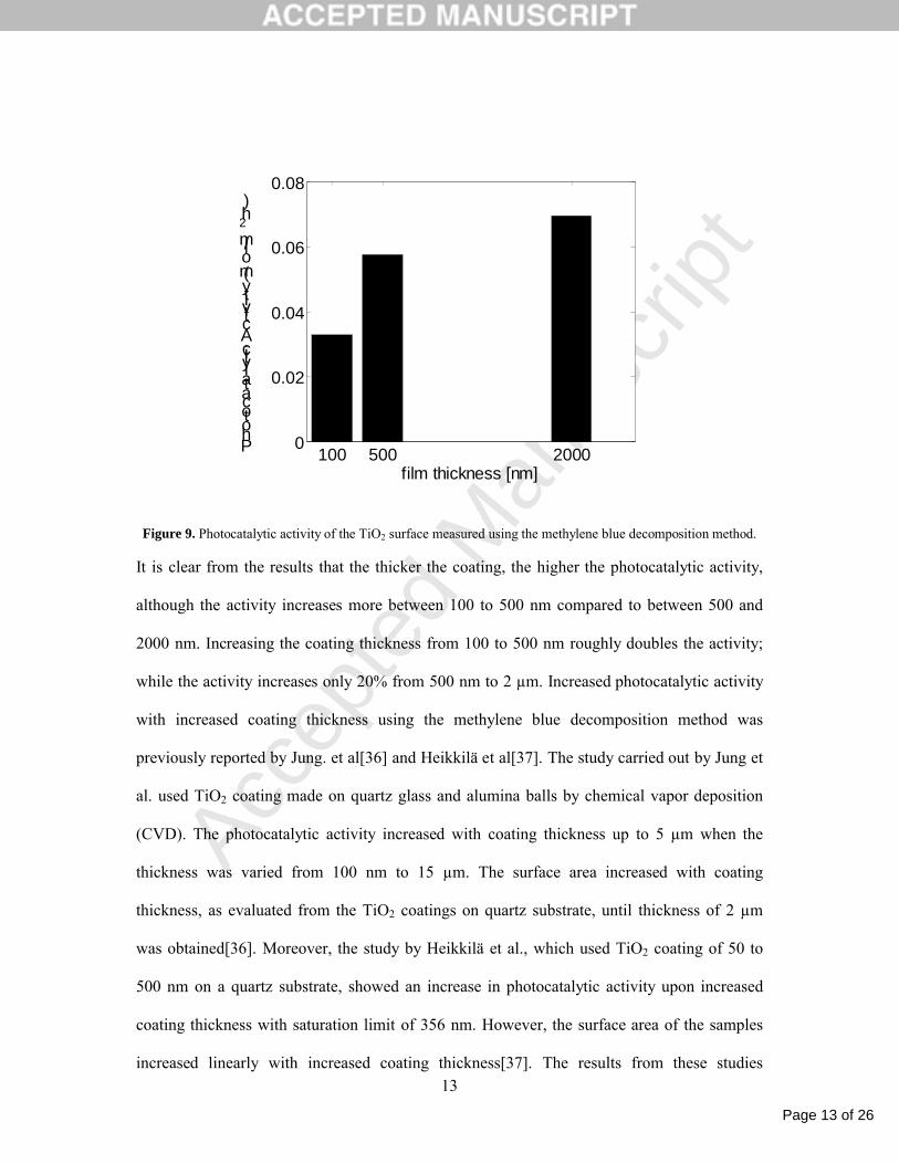
3.2.1 Decomposition of methylene blue as a function of time Figure 9 shows the decomposition of the methylene blue by TiO2 coatings with UV-
illumination measured over a period of three hours. The results represent the net
decomposition of the indicator with UV light and were obtained by subtracting the level of
decomposition caused by the absorption of the indictor into TiO2 film by measuring in the
absence of the UV-light.
[nm]
A) B)
Page 13 of 26
Accep
ted
Man
uscr
ipt
13
Figure 9. Photocatalytic activity of the TiO2 surface measured using the methylene blue decomposition method.
It is clear from the results that the thicker the coating, the higher the photocatalytic activity,
although the activity increases more between 100 to 500 nm compared to between 500 and
2000 nm. Increasing the coating thickness from 100 to 500 nm roughly doubles the activity;
while the activity increases only 20% from 500 nm to 2 µm. Increased photocatalytic activity
with increased coating thickness using the methylene blue decomposition method was
previously reported by Jung. et al[36] and Heikkilä et al[37]. The study carried out by Jung et
al. used TiO2 coating made on quartz glass and alumina balls by chemical vapor deposition
(CVD). The photocatalytic activity increased with coating thickness up to 5 µm when the
thickness was varied from 100 nm to 15 µm. The surface area increased with coating
thickness, as evaluated from the TiO2 coatings on quartz substrate, until thickness of 2 µm
was obtained[36]. Moreover, the study by Heikkilä et al., which used TiO2 coating of 50 to
500 nm on a quartz substrate, showed an increase in photocatalytic activity upon increased
coating thickness with saturation limit of 356 nm. However, the surface area of the samples
increased linearly with increased coating thickness[37]. The results from these studies
100 500 20000
0.02
0.04
0.06
0.08
film thickness [nm]
Photocatalytic Activity (mol/m
2 h)
Page 14 of 26
Accep
ted
Man
uscr
ipt
14
indicate that the surface area partially influences the photocatalytic activity by providing more
reaction sites on the surface for the photocatalytic reaction. However, the change in
photocatalytic activity does not follow the same trend as the change in surface area upon
increased TiO2 coating thickness, which strongly suggests that the surface area is not the only
parameter influencing the photocatalytic activity.
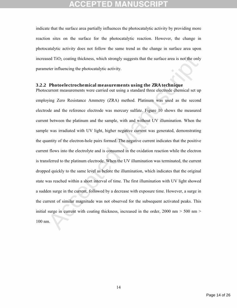
3.2.2 Photoelectrochemical measurements using the ZRA techniquePhotocurrent measurements were carried out using a standard three electrode chemical set up
employing Zero Resistance Ammetry (ZRA) method. Platinum was used as the second
electrode and the reference electrode was mercury sulfate. Figure 10 shows the measured
current between the platinum and the sample, with and without UV illumination. When the
sample was irradiated with UV light, higher negative current was generated, demonstrating
the quantity of the electron-hole pairs formed. The negative current indicates that the positive
current flows into the electrolyte and is consumed in the oxidation reaction while the electron
is transferred to the platinum electrode. When the UV illumination was terminated, the current
dropped quickly to the same level as before the illumination, which indicates that the original
state was reached within a short interval of time. The first illumination with UV light showed
a sudden surge in the current, followed by a decrease with exposure time. However, a surge in
the current of similar magnitude was not observed for the subsequent activated peaks. This
initial surge in current with coating thickness, increased in the order, 2000 nm > 500 nm >
100 nm.
Page 15 of 26
Accep
ted
Man
uscr
ipt
15
Figure 10. The current measurements of TiO2 coating on aluminium with time. The sample was activated three
times with UV light for 15 min each time with 45 min break between the excitations.
Similarly, the magnitude of the plateau current generated by the UV illumination was
significantly lower for the 100 nm coatings compared to the 500 nm and 2000 nm samples,
while the difference was negligible between the 500 nm and 2 micron samples. Table 1 shows
the total charge after the last illumination, which was obtained by integrating the area under
the curve. The total charge remained the same for the 500 and 2000 nm samples, while the
100 nm sample showed less charge. The magnitude of the current and total charge
corresponds to the efficiency of the photocatalytic process.
Table 1. The charging accruing in the TiO2 coating (the integral of the current/time plot, Figure 10).
100 nm 500 nm 2000 nm
-0.8 mC/cm2 -1.2mC/·cm2 -1.3 mC/·cm2
Page 16 of 26
Accep
ted
Man
uscr
ipt
16
3.2.3 Electrical properties of TiO2
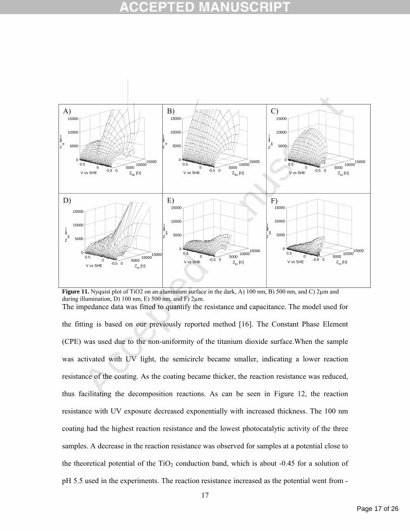
Impedance measurements were carried out to evaluate the electrical properties of TiO2,
including the reaction resistance and capacitance behaviour with increased coating thickness
on the aluminium substrate. The reaction resistance upon illumination is of special interest
due to its connection with the consumption of electrons and holes on the surface of the
titanium dioxide. When the reaction resistance is lower than the photo-generated resistance,
holes are consumed faster, forming hydroxide radicals. The impedance measurements were
taken at various potential values corresponding to different positions within the band gap of
TiO2. The potential window used for the measurement was between -0.4 V (just below the
theoretical conduction band of TiO2) and 0.75 V. The results are presented as a Nyquist plot
in Figure 11, and the capacitance and the resistance can be extracted from the semicircles. The
top and bottom panels represent sample without and with UV light, respectively. The entire
impedance spectra consist of a semicircle, but the dimension and nature of the semicircle
vary. The diameter of the semicircle is a measure of the reaction resistance. When the sample
was excited with UV-light, the size of the semicircle decreased, indicating that the reaction
resistance decreased.
Page 17 of 26
Accep
ted
Man
uscr
ipt
17
Figure 11. Nyquist plot of TiO2 on an aluminium surface in the dark, A) 100 nm, B) 500 nm, and C) 2µm and during illumination, D) 100 nm, E) 500 nm, and F) 2µm.The impedance data was fitted to quantify the resistance and capacitance. The model used for
the fitting is based on our previously reported method [16]. The Constant Phase Element
(CPE) was used due to the non-uniformity of the titanium dioxide surface.When the sample
was activated with UV light, the semicircle became smaller, indicating a lower reaction
resistance of the coating. As the coating became thicker, the reaction resistance was reduced,
thus facilitating the decomposition reactions. As can be seen in Figure 12, the reaction
resistance with UV exposure decreased exponentially with increased thickness. The 100 nm
coating had the highest reaction resistance and the lowest photocatalytic activity of the three
samples. A decrease in the reaction resistance was observed for samples at a potential close to
the theoretical potential of the TiO2 conduction band, which is about -0.45 for a solution of
pH 5.5 used in the experiments. The reaction resistance increased as the potential went from -
05000
1000015000
-0.50
0.50
5000
10000
15000
ZRe
[]V vs SHE
ZIm
[]
05000
1000015000
-0.50
0.50
5000
10000
15000
ZRe
[]V vs SHE
ZIm
[]
05000
1000015000
-0.50
0.50
5000
10000
15000
ZIm
[]V vs SHE
ZRe [
]
05000
1000015000
-0.50
0.50
5000
10000
15000
ZIm
[]V vs SHE
ZRe [
]
05000
1000015000
-0.50
0.50
5000
10000
15000
ZIm
[]V vs SHE
ZRe [
]
05000
1000015000
-0.50
0.50
5000
10000
15000
ZIm
[]V vs SHE
ZRe [
]
A) B) C)
D) E) F)
Page 18 of 26
Accep
ted
Man
uscr
ipt
18
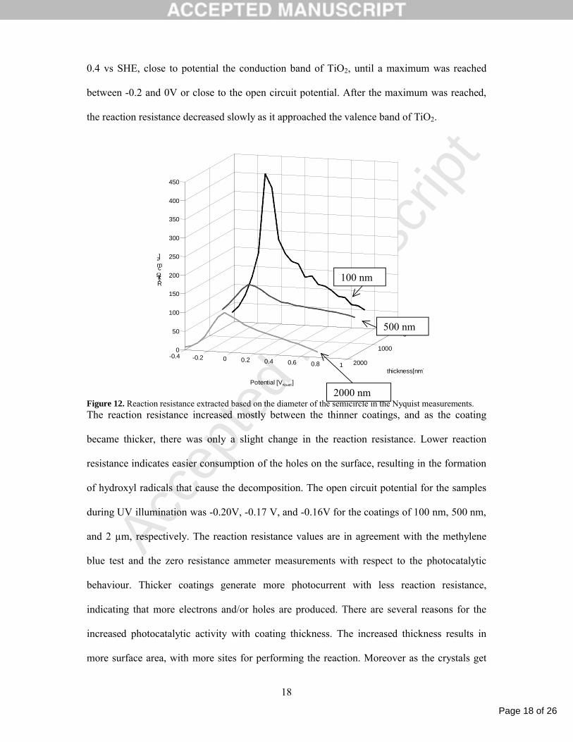
0.4 vs SHE, close to potential the conduction band of TiO2, until a maximum was reached
between -0.2 and 0V or close to the open circuit potential. After the maximum was reached,
the reaction resistance decreased slowly as it approached the valence band of TiO2.
0
1000
2000-0.4 -0.2 0 0.2 0.4 0.6 0.8 1
0
50
100
150
200
250
300
350
400
450
thickness[nm]
Potential [VSHE]
R[k cm2]
Figure 12. Reaction resistance extracted based on the diameter of the semicircle in the Nyquist measurements.The reaction resistance increased mostly between the thinner coatings, and as the coating
became thicker, there was only a slight change in the reaction resistance. Lower reaction
resistance indicates easier consumption of the holes on the surface, resulting in the formation
of hydroxyl radicals that cause the decomposition. The open circuit potential for the samples
during UV illumination was -0.20V, -0.17 V, and -0.16V for the coatings of 100 nm, 500 nm,
and 2 µm, respectively. The reaction resistance values are in agreement with the methylene
blue test and the zero resistance ammeter measurements with respect to the photocatalytic
behaviour. Thicker coatings generate more photocurrent with less reaction resistance,
indicating that more electrons and/or holes are produced. There are several reasons for the
increased photocatalytic activity with coating thickness. The increased thickness results in
more surface area, with more sites for performing the reaction. Moreover as the crystals get
100 nm
500 nm
2000 nm

Page 19 of 26
Accep
ted
Man
uscr
ipt
19
larger, the hole/electron recombination is reduced[23]. Furthermore, increased thickness
results in increased UV absorption until saturation depths have been reached. The saturation
depth for PVD-synthesized TiO2 coatings used in the present investigation has been reported
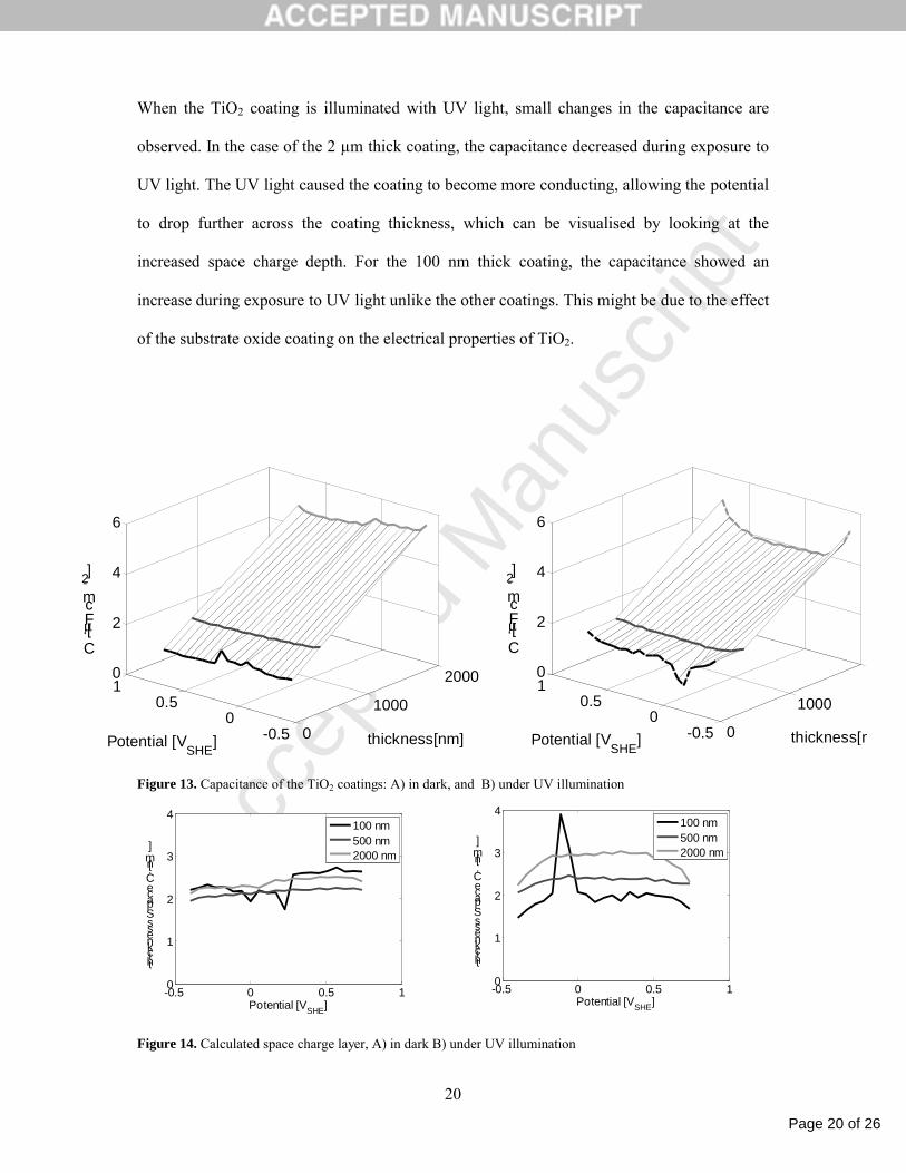
to be around 1 µm[17]. Figure 13 shows the change in capacitance of the coatings with and
without UV light exposure. The capacitance of the TiO2 coatings increased linearly with
increased coating thickness in the absence of UV light, which indicates that the potential
drops across the space charge region rather than across the entire coating thickness as is
characteristic in semiconductors. The space charge region is close to the surface where the CB
and VB bend upward to adjust to the redox potential of the electrolyte. The relationship
between the capacitance, surface roughness, dielectric constant and space charge distance can
be seen in equation (5).
(5)
Where C is the space charge capacitance, is the relative permittivity (dielectric constant)
and is the permittivity of the free space, A is the total surface area (calculated from the
surface area ratio acquired from AFM), and L is the depth of the space charge region for a
semiconductor[38]. The surface area of the sample and its dielectric constant increased
linearly with increased coating thickness, following the same trend as the capacitance. The
depth of the space charge region was calculated by rearranging equation 5. The space charge
layer of the samples as a function of thickness can be seen in Figure 14, in the dark (A) and
under illumination (B). The layer was approximately 2 nm for all samples, with increased
slope for higher potential. The typical range of space charge thickness of thin coatings in
semiconductors is between 1-103nm[39]. Moreover, it was reported by Tiejun and al. that the
best superficial space charge layer thickness of TiO2 was about 2 nm and the thickness of the
layer decreased with increased amount of ion doping [40].
Page 20 of 26
Accep
ted
Man
uscr
ipt
20
When the TiO2 coating is illuminated with UV light, small changes in the capacitance are
observed. In the case of the 2 µm thick coating, the capacitance decreased during exposure to
UV light. The UV light caused the coating to become more conducting, allowing the potential
to drop further across the coating thickness, which can be visualised by looking at the
increased space charge depth. For the 100 nm thick coating, the capacitance showed an
increase during exposure to UV light unlike the other coatings. This might be due to the effect
of the substrate oxide coating on the electrical properties of TiO2.
0
1000
2000
-0.50
0.510
2
4
6
thickness[nm]Potential [VSHE
]
C [F cm-2]
0
1000
-0.50
0.510
2
4
6
thickness[nm]Potential [VSHE
]
C [F cm-2]
Figure 13. Capacitance of the TiO2 coatings: A) in dark, and B) under UV illumination
Figure 14. Calculated space charge layer, A) in dark B) under UV illumination
-0.5 0 0.5 10
1
2
3
4
Potential [VSHE]
thickness Space C. [n
m]
100 nm500 nm2000 nm
-0.5 0 0.5 10
1
2
3
4
Potential [VSHE]
thickness Space C.[n
m]
100 nm500 nm2000 nm
Page 21 of 26
Accep
ted
Man
uscr
ipt
21
4 Conclusions
1. The magnetron-sputtered TiO2 coatings on aluminium alloy 1050 showed columnar
growth of the coating with crystallite size increasing with increase in thickness of the
coating. The results also showed a quasi-linear dependency between the crystallites
in-plane size, thickness, and increase in surface area with respect to the synthesis time.
2. The refractive index increased linearly with the coating thickness, demonstrating
increased density with coating thickness.
3. The methylene blue decomposition test showed an increase in photocatalytic activity
with increased coating thickness, which was greater for the thickness range of 100 nm
and 500 nm compared to the increase between 500 nm and 2 µm.
4. The photo-electrochemical test using zero resistance ammetry method showed an
increase in photocurrent under UV illumination, with the magnitude of the current
increasing with increased thickness of the coating. Similar to the results from the
decomposition studies, the difference in photocurrent was higher for coating thickness
between 100 nm and 500 nm, while the difference was negligible between 500 nm and
2 µm thick coatings.
5. The impedance measurements showed a decrease in reaction resistance with coating
thickness, indicating more photocatalytic activity for thicker samples. The difference
is more obvious in terms of the reaction resistance between the 100 and 500 nm
coatings than between the 500 nm and 2 µm coatings.
6. The space charge capacitance of the coating increased linearly with increased
thickness when there was no UV exposure. During UV-illumination the capacitance
changed only slightly compared with capacitance in the dark for a given coating
thickness.
Page 22 of 26
Accep
ted
Man
uscr
ipt
22
Acknowledgements
The authors would like to thank Juliano Soyama for help with the methylene blue testing and Torben Jacobsen for assistance with the impedance work. Authors would like to acknowledge funding from the Danish Advanced Technology Foundation AMAS project and SETNanoMetro, EU Project. R. Shabadi would like to thank BQR-3b 2014-Univ Lille1 for the financial support for this collaboration.. ACG acknowledges Romanian Ministry of Education - PN-II-RU-TE-2011-3-0016 Project - for financial support.
References
[1] M. Grätzel, “Photoelectrochemical cells,” Nature, vol. 414, pp. 338–344, 2001.
[2] A. Fujishima, T. N. Rao, and D. a. Tryk, “Titanium dioxide photocatalysis,” J. Photochem. Photobiol. C Photochem. Rev., vol. 1, no. 1, pp. 1–21, Jun. 2000.
[3] X. Chen and S. S. Mao, “Titanium dioxide nanomaterials: synthesis, properties, modifications, and applications.,” Chem. Rev., vol. 107, no. 7, pp. 2891–959, Jul. 2007.
[4] M. M. Ballari, M. Hunger, G. Hüsken, and H. J. H. Brouwers, “NOx photocatalytic degradation employing concrete pavement containing titanium dioxide,” Appl. Catal. B Environ., vol. 95, no. 3–4, pp. 245–254, Apr. 2010.
[5] J. Gamage and Z. Zhang, “Applications of Photocatalytic Disinfection,” Int. J. Photoenergy, vol. 2010, pp. 1–11, 2010.
[6] A. Fujishima, X. Zhang, and D. A. Tryk, “TiO2 photocatalysis and related surface phenomena,” Surf. Sci. Rep., vol. 63, no. 12, pp. 515–582, Dec. 2008.
[7] O. Carp, “Photoinduced reactivity of titanium dioxide,” Prog. Solid State Chem., vol. 32, no. 1–2, pp. 33–177, 2004.
[8] I. P. Parkin and R. G. Palgrave, “Self-cleaning coatings,” J. Mater. Chem., vol. 15, no. 17, p. 1689, 2005.
[9] V. Augugliaro, V. Loddo, M. Pagliaro, G. Palmisano, and L. Palmisano, Clean by Light Irradiation: Practical Applications of Supported TiO2. Cambridge (UK): RSC Publishing, 2010, pp. 2–5.
[10] A. Selloni, “Anatase shows its reactive side,” Water, vol. 7, no. August, pp. 613–615, 2008.
[11] X.-Q. Gong and A. Selloni, “Reactivity of anatase TiO(2) nanoparticles: the role of the minority (001) surface.,” J. Phys. Chem. B, vol. 109, no. 42, pp. 19560–2, Oct. 2005.
[12] H. G. Yang, C. H. Sun, S. Z. Qiao, J. Zou, G. Liu, S. C. Smith, H. M. Cheng, and G. Q. Lu, “Anatase TiO2 single crystals with a large percentage of reactive facets.,” Nature, vol. 453, no. 7195, pp. 638–41, May 2008.
Page 23 of 26
Accep
ted
Man
uscr
ipt
23
[13] K. Wilke, “The influence of transition metal doping on the physical and photocatalytic properties of titania,” J. Photochem. Photobiol. A Chem., vol. 121, no. 1, pp. 49–53, Feb. 1999.
[14] T. Umebayashi, “Analysis of electronic structures of 3d transition metal-doped TiO2 based on band calculations,” J. Phys. Chem. Solids, vol. 63, no. 10, pp. 1909–1920, Oct. 2002.
[15] U. Diebold, “The surface science of titanium dioxide,” Surf. Sci. Rep., vol. 48, no. 5–8, pp. 53–229, Jan. 2003.
[16] S. Daviðsdóttir, S. Canulescu, K. Dirscherl, J. Schou, and R. Ambat, “Investigation of photocatalytic activity of titanium dioxide deposited on metallic substrates by DC magnetron sputtering,” Surf. Coatings Technol., vol. 216, pp. 35–45, Nov. 2013.
[17] S. Daviðsdóttir, K. Dirscherl, R. Shabadi, S. Canulescu, and R. Ambat, “Nanoscale surface potential imaging of the photocatalytic TiO2 films on aluminum,” RSC Adv., vol. 3, pp. 23296–23302, 2013.
[18] K. Jung, “Anatase-phase titania: preparation by embedding silica and photocatalytic activity for the decomposition of trichloroethylene,” J. Photochem. Photobiol. A Chem., vol. 127, no. 1–3, pp. 117–122, Oct. 1999.
[19] Y.-J. Cheng and J. S. Gutmann, “Morphology phase diagram of ultrathin anatase TiO2 films templated by a single PS-b-PEO block copolymer.,” J. Am. Chem. Soc., vol. 128, no. 14, pp. 4658–74, Apr. 2006.
[20] M. G. Nielsen, S.-I. In, P. C. K. Vesborg, T. Pedersen, K. P. Almtoft, I. H. Andersen, O. Hansen, and I. Chorkendorff, “A generic model for photocatalytic activity as a function of catalyst thickness,” J. Catal., vol. 289, pp. 62–72, May 2012.
[21] C. Giolli, G. Rizzi, A. Scrivani, R. Ferpozzi, S. Troglio, M. M. Miranda, A. Tolstoguzov, U. Bardi, F. Borgioli, A. Fossati, A. Credi, A. Di Fabio, S. Parmeggiani, A. Zoppi, A. Scrivani, R. Ferpozzi, M. M. Miranda, Ad. Fabio, S. Parmeggiani, and A. Zoopi, “Development and characterization of TiO2 coatings prepared by electric arc-physical vapour deposition system,” Surf. Eng., pp. 27–36, 2008.
[22] A. C. Galca, G. E. Stan, L. M. Trinca, C. C. Negrila, and L. C. Nistor, “Structural and optical properties of c-axis oriented aluminum nitride thin films prepared at low temperature by reactive radio-frequency magnetron sputtering,” Thin Solid Films, vol. 524, pp. 328–333, Dec. 2012.
[23] K. Y. Jung, S. Bin Park, and S.-K. Ihm, “Linear relationship between the crystallite size and the photoactivity of non-porous titania ranging from nanometer to micrometer size,” Appl. Catal. A Gen., vol. 224, no. 1–2, pp. 229–237, Jan. 2002.
[24] D. Norm, “DIN 52980:2008–10: Photokatalytische Aktivität von Oberflächen—Bestimmung der photokatalytischen Aktivität durch Abbau von Methylenblau,” 2008.
[25] A. Wold, “Photocatalytic properties of titanium dioxide (TiO2),” Chem. Mater., vol. 5, no. 3, pp. 280–283, Mar. 1993.
Page 24 of 26
Accep
ted
Man
uscr
ipt
24
[26] R. Messier, “Revised structure zone model for thin film physical structure,” J. Vac. Sci. Technol. A Vacuum, Surfaces, Film., vol. 2, no. 2, p. 500, 1984.
[27] O. Kluth, G. Schöpe, J. Hüpkes, C. Agashe, J. Müller, and B. Rech, “Modified Thornton model for magnetron sputtered zinc oxide: film structure and etching behaviour,” Thin Solid Films, vol. 442, no. 1–2, pp. 80–85, Oct. 2003.
[28] J. A. Thornton, “High rate thick film,” Annu. Rev. Mater. Sci., vol. 7, pp. 239–260, 1977.
[29] A. B. Rodriguez-Navarro, “Model of texture development in polycrystalline films growing on amorphous substrates with different topographies,” Thin Solid Films, vol. 389, no. 1–2, pp. 288–295, Jun. 2001.
[30] A. C. Galca, V. Stancu, M. a. Husanu, C. Dragoi, N. G. Gheorghe, L. Trupina, M. Enculescu, and E. Vasile, “Substrate–target distance dependence of structural and optical properties in case of Pb(Zr,Ti)O3 films obtained by pulsed laser deposition,” Appl. Surf. Sci., vol. 257, no. 14, pp. 5938–5943, May 2011.
[31] S. Tanemura, L. Miao, P. Jin, K. Kaneko, a. Terai, and N. Nabatova-Gabain, “Optical properties of polycrystalline and epitaxial anatase and rutile TiO2 thin films by rf magnetron sputtering,” Appl. Surf. Sci., vol. 212–213, pp. 654–660, May 2003.
[32] H. K. Pulker and S. S. Schlichtherle, “Density Related Properties of Metal Oxide Films,” vol. 5250, pp. 1–11, Feb. 2004.
[33] D. M. Mattox, Handbook of Physical Vapor Deposition (PVD) Processing, Second edi. Elsevier, 2010, pp. 333–398.
[34] G. Abadias, W. P. Leroy, S. Mahieu, and D. Depla, “Influence of particle and energy flux on stress and texture development in magnetron sputtered TiN films,” J. Phys. D. Appl. Phys., vol. 46, no. 5, p. 055301, Feb. 2013.
[35] A. Le Febvrier, A. C. Galca, Y. Corredores, S. De, D. Rennes, U. De Rennes, and I. U. T. De Saint-brieuc, “Structural, Optical, and Dielectric Properties of Bi 1.5 −,” Appl. Mater. interfaces, vol. 4, pp. 5227–5233, 2012.
[36] S.-C. Jung, S.-J. Kim, N. Imaishi, and Y.-I. Cho, “Effect of TiO2 thin film thickness and specific surface area by low-pressure metal–organic chemical vapor deposition on photocatalytic activities,” Appl. Catal. B Environ., vol. 55, no. 4, pp. 253–257, Feb. 2005.
[37] M. Heikkilä, E. Puukilainen, M. Ritala, and M. Leskelä, “Effect of thickness of ALD grown TiO2 films on photoelectrocatalysis,” J. Photochem. Photobiol. A Chem., vol. 204, no. 2–3, pp. 200–208, May 2009.
[38] D. . Blackwood, “Influence of the space-charge region on electrochemical impedance measurements on passive oxide films on titanium,” Electrochim. Acta, vol. 46, no. 4, pp. 563–569, Dec. 2000.
Page 25 of 26
Accep
ted
Man
uscr
ipt
25
[39] K. Hashimoto, H. Irie, and A. Fujishima, “TiO 2 Photocatalysis: A Historical Overview and Future Prospects,” Jpn. J. Appl. Phys., vol. 44, no. No. 12, pp. 8269–8285, Dec. 2005.
[40] C. A. I. Tiejun, L. Yuchao, P. Zhenshan, L. Yunfei, W. E. I. Zongyuan, and D. Qian, “Photocatalytic performance of TiO2 catalysts modified by H3PW12O40, ZrO2 and CeO2,” J. en, vol. 21, pp. 997–1004, 2008.
Page 26 of 26
Accep
ted
Man
uscr
ipt
26
7. The magnetron-sputtered TiO2 coatings on aluminium alloy 1050 showed columnar
growth of the coating with crystallite size increasing with increase in thickness of the
coating. The results also showed a quasi-linear dependency between the crystallites
in-plane size, thickness, and increase in surface area with respect to the synthesis time.
8. The refractive index increased linearly with the coating thickness, demonstrating
increased density with coating thickness.
9. The methylene blue decomposition test showed an increase in photocatalytic activity
with increased coating thickness, which was greater for the thickness range of 100 nm
and 500 nm compared to the increase between 500 nm and 2 µm.
10. The photo-electrochemical test using zero resistance ammetry method showed an
increase in photocurrent under UV illumination, with the magnitude of the current
increasing with increased thickness of the coating. Similar to the results from the
decomposition studies, the difference in photocurrent was higher for coating thickness
between 100 nm and 500 nm, while the difference was negligible between 500 nm and
2 µm thick coatings.
11. The impedance measurements showed a decrease in reaction resistance with coating
thickness, indicating more photocatalytic activity for thicker samples. The difference
is more obvious in terms of the reaction resistance between the 100 and 500 nm
coatings than between the 500 nm and 2 µm coatings.
12. The space charge capacitance of the coating increased linearly with increased
thickness when there was no UV exposure. During UV-illumination the capacitance
changed only slightly compared with capacitance in the dark for a given coating
thickness.


![Phase stability of AlYB14 sputtered thin filmshenkelmanlab.org/pubs/kolpin09_355006.pdf · AlxYyB14 samples were synthesized by magnetron sputtering within a combinatorial setup [12]](https://img.pdfslide.us/doc/110x75/5e4bb86a8d90841bf1702312/phase-stability-of-alyb14-sputtered-thin-alxyyb14-samples-were-synthesized-by-magnetron.jpg)