Embed Size (px)
Citation preview

Chem. Met. Alloys 3 (2010) 1
Chem. Met. Alloys 3 (2010) 1-4 Ivan Franko National University of Lviv
www.chemetal-journal.org
Investigation of CdSb surfaces after different processing methods S.G. DREMLYUZHENKO1* 1 Yuriy Fedkovych Chernivtsi National University, Kotsyubynskyy St. 2, 58012 Chernivtsi, Ukraine * Corresponding author. Tel.: +380-37-2584893; e-mail: [email protected] Received January 19, 2010; accepted June 29, 2010; available on-line November 5, 2010 The effect of different processing methods on the surface of CdSb crystals has been studied. Studies by the electron Auger-spectroscopy method have shown the presence of etchant components in the near-surface oxide layer. Chemical-mechanical polishing with an alkaline solution of colloidal silica allows obtaining an oxide layer of minimum thickness and a contaminated surface of close to stoichiometric composition. Mechanical polishing / Chemical treatment / Chemical-mechanical polishing / CdSb / Surface / Damaged layer Introduction Obtaining perfect surfaces of AIIBV type semiconductor crystals is an important technological challenge that can expand their application area and improve the performance of devices. However, as compared to AIV, AIIIBV and AIIBVI semiconductors, metal processing technology and, especially, final surface polishing of AIIBV semiconductors is little known and poorly developed [1-3]. Cadmium antimonide (CdSb) is used to manufacture various-purpose thermoelectric devices and as a basic substrate material for obtaining photosensitive epitaxial structures and cut-off interference-absorption filters [4-6]. Etching CdSb and alloys on its basis is a redox process that occurs at a “semiconductor-electrolyte” interface [7]. The practical task of selecting the composition of etchants is reduced to the analysis of the chemical stability of CdSb and its oxidation products in aqueous media at different рН values. This task is solved by methods of chemical thermodynamics, through calculation and construction of the ϕ–рН diagram (Pourbaix diagram) for the CdSb–H2O system. The ϕ–рН diagram was constructed with the use of methods for combining the simple diagrams Cd–H2O and Sb–H2O [8], taking into account the solid-state reaction Cd + Sb = CdSb. From the examination of the CdSb–Н2О diagram it follows that for each value of the potential the mechanism of CdSb oxidation is defined by the pН value. With regard to the characteristics of the etchants [2,9], it can be considered that the results of the analysis of the ϕ–рН diagram allow explaining the mechanism of interaction between CdSb and
solutions of already known compositions, as well as predicting and creating new compositions of etchants. In the course of treatment of semiconductor plates and crystals, the depth of the damaged layer should be controlled efficiently, to avoid violation of technological process conditions. Therefore, the development and introduction of methods for express control and estimation of the damaged layer are of particular importance. The main target at the stage of surface preparation is removal of the damaged layer that results from crystal cutting. Partial removal of the damaged layer occurs during crystal polishing by loose or bound abrasive. Mechanical polishing also results in a damaged layer, finishing generally includes mechanical, chemical, chemical-mechanical polishing [10]. Results and discussion The depth of the damaged layer produced by cutting, as estimated in [11], is 120 µm. Polishing was made using M5 micropowder. In the course of mechanical polishing, free abrasive was used to remove a 60÷80 µm layer (Fig. 1а). Polishing with diamond pastes was made on a polisher covered with satin or silk, uniformly coated with a thin layer of АSM 5/3, АSM 3/2, or АSM 1/0 paste. The total thickness of the layer removed in the course of polishing was 40÷60 µm. As a result of these operations, one cannot obtain a surface that meets the requirements of structure perfection, pattern and cleanness. It was established that the depth of the damaged layer is proportional to the grain size of the abrasive material and depends on the crystallographic

S.G. Dremlyuzhenko, Investigation of CdSb surfaces after different processing methods
Chem. Met. Alloys 3 (2010) 2
(a)
(b)
(c)
Fig. 1 Morphology of a CdSb single crystal surface obtained by (secondary electrons on REM-100U): (а) polishing with M5 micropowder; (b) mechanical polishing with АSM 1/0 diamond paste; (c) chemical-mechanical polishing with a SiO2 alkaline solution.
orientation of the processed surface (d100> d001> d010), which is attributable to the anisotropy of the microhardness of CdSb crystals [1,2]. Electron microscope studies show the presence of scratches, abrasive inclusions, surface irregularities that are particularly emphasized by a survey in Y-modulation mode (Fig. 1) [12]. The simplest method for removal of the damaged layer is deep chemical etching. However, X-ray methods have shown an increase of the surface roughness after etching [2,11]. It is due to the fact that the pattern of damaged layer bands with penetration deep into the crystal retains in full measure the surface pattern [10]. The rates of chemical etching in the planes (100), (010), and (001) of the same composition are somewhat different. However, this factor is smoothed out by agitation of the etching mixture. The chemical etchant first of all removes the
damaged parts of the single crystal. This results in a surface with deep holes, if the surface had preliminarily been ground or polished, with a depth of relief comparable to the grain size of the abrasive used. Consequently, chemical-mechanical polishing with a colloidal silica solution was selected as the final processing step. For chemical-mechanical polishing [10], the basis for material removal from the processed surface is a series of chemical reactions. The dynamic mode of chemical-mechanical polishing results in a uniform distribution of reagents and reaction products in the bulk of the solution, thus creating optimal conditions for the polishing effect. An essential technological factor that affects the quality and status of the processed surface is the presence in the etching solution of highly dispersed (2÷20 nm) modified aerosol that performs the functions of an abrasive and
20 µµµµm
20 µµµµm 100 µµµµm

S.G. Dremlyuzhenko, Investigation of CdSb surfaces after different processing methods
Chem. Met. Alloys 3 (2010) 3
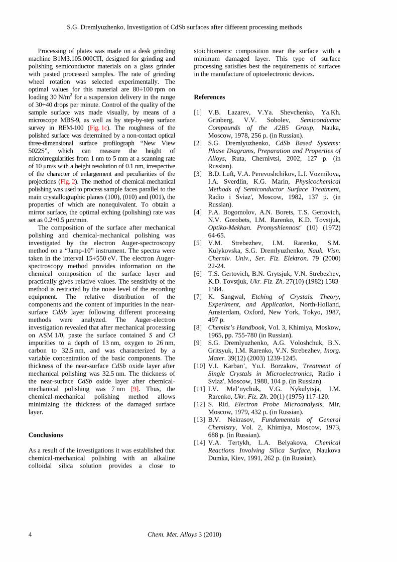
Fig. 2 Roughness parameters and microstructure of a CdSb (100) surface obtained by chemical-mechanical polishing with an alkaline solution of colloidal silica.
a complexing agent. As a result of this, the abrasive SiO2 grains remove loosened surface layer that has much lower hardness than the initial material. This accounts for a higher efficiency of chemical-mechanical polishing as compared to mechanical polishing. Chemical-mechanical polishing allows obtaining plates with a minimum damaged layer free from the “diamond background”. The presence on the surface of a modified aerosol of absorption-active –ОН and –NH2 groups contributes to the removal of solution products from the reaction zone, thanks to which the thickness of the diffusion layer is reduced and favorable conditions for obtaining a high-quality surface are created (Fig. 1). The result of chemical-mechanical polishing of CdSb substrates with a colloidal silica solution is determined by the rate of the chemical reaction on the semiconductor surface, and the efficiency of delivery of reagents and removal of reaction products. Parameters that can affect the degree of removal and the quality of the surface are: the concentration of oxidizer (Н2О2), specific pressure on the substrate, temperature in the processing zone, number of microirregularities, processing time. Increase of the chemical activity of the suspension and oxidizer concentration results in increasing etching rate. Rise of the temperature in the course of etching also contributes to a greater etching rate. The optimal temperature range in our investigations was 293÷300 K. Uncontrolled temperature rise leads to decomposition of the oxidizer
and cessation of the chemical-mechanical processing. At temperatures lower than 293 K, the mechanical interaction, as compared to the chemical interaction, is prevalent on the surface. Increase of the polishing time also leads to a reduction of the polishing rate and leveling efficiency; as long as the surface irregularities are polished and the damaged layer is removed after the preliminary processing, the rate of chemical interaction drops and the effect of the mechanical factor is simultaneously increased. Prolonged stay in corrosive medium can also result in overetching of the substrate surface. Due to its hydrophilic nature, silica can easily be introduced into aqueous media, and stable aqueous dispersions can be obtained. The products formed during polishing are removed from the surface due to the absorption ability caused by the highly developed silica surface. Formation of silicon peroxide compounds is not typical, and superacid derivatives of silicon were not obtained [13]. Addition of glycerin to the etchant made it possible to increase the viscosity of the solution, reduce the diffusion of reacting etchant components and optimize the etching velocity. Another positive factor of the introduction of glycerin to the etching solution is that it serves as a complexing agent, thus bonding, in combination with silica, the etching products and converting them into a solution. Adding monoethanolamine to the solution causes modification of the aerosol, reinforcing its complexing properties [14].
S.G. Dremlyuzhenko, Investigation of CdSb surfaces after different processing methods
Chem. Met. Alloys 3 (2010) 4
Processing of plates was made on a desk grinding machine В1МЗ.105.000СП, designed for grinding and polishing semiconductor materials on a glass grinder with pasted processed samples. The rate of grinding wheel rotation was selected experimentally. The optimal values for this material are 80÷100 rpm on loading 30 N/m2 for a suspension delivery in the range of 30÷40 drops per minute. Control of the quality of the sample surface was made visually, by means of a microscope МBS-9, as well as by step-by-step surface survey in RЕМ-100 (Fig. 1c). The roughness of the polished surface was determined by a non-contact optical three-dimensional surface profilograph “New View 5022S”, which can measure the height of microirregularities from 1 nm to 5 mm at a scanning rate of 10 µm/s with a height resolution of 0.1 nm, irrespective of the character of enlargement and peculiarities of the projections (Fig. 2). The method of chemical-mechanical polishing was used to process sample faces parallel to the main crystallographic planes (100), (010) and (001), the properties of which are nonequivalent. To obtain a mirror surface, the optimal etching (polishing) rate was set as 0.2÷0.5 µm/min. The composition of the surface after mechanical polishing and chemical-mechanical polishing was investigated by the electron Auger-spectroscopy method on a “Jamp-10” instrument. The spectra were taken in the interval 15÷550 eV. The electron Auger-spectroscopy method provides information on the chemical composition of the surface layer and practically gives relative values. The sensitivity of the method is restricted by the noise level of the recording equipment. The relative distribution of the components and the content of impurities in the near-surface CdSb layer following different processing methods were analyzed. The Auger-electron investigation revealed that after mechanical processing on АSМ 1/0, paste the surface contained S and Cl impurities to a depth of 13 nm, oxygen to 26 nm, carbon to 32.5 nm, and was characterized by a variable concentration of the basic components. The thickness of the near-surface CdSb oxide layer after mechanical polishing was 32.5 nm. The thickness of the near-surface CdSb oxide layer after chemical-mechanical polishing was 7 nm [9]. Thus, the chemical-mechanical polishing method allows minimizing the thickness of the damaged surface layer. Conclusions As a result of the investigations it was established that chemical-mechanical polishing with an alkaline colloidal silica solution provides a close to
stoichiometric composition near the surface with a minimum damaged layer. This type of surface processing satisfies best the requirements of surfaces in the manufacture of optoelectronic devices. References [1] V.B. Lazarev, V.Ya. Shevchenko, Ya.Kh.
Grinberg, V.V. Sobolev, Semiconductor Compounds of the А2B5 Group, Nauka, Moscow, 1978, 256 p. (in Russian).
[2] S.G. Dremlyuzhenko, CdSb Based Systems: Phase Diagrams, Preparation and Properties of Alloys, Ruta, Chernivtsi, 2002, 127 p. (in Russian).
[3] B.D. Luft, V.A. Perevoshchikov, L.I. Vozmilova, I.A. Sverdlin, K.G. Marin, Physicochemical Methods of Semiconductor Surface Treatment, Radio i Sviaz', Moscow, 1982, 137 p. (in Russian).
[4] P.A. Bogomolov, A.N. Borets, T.S. Gertovich, N.V. Gorobets, I.M. Rarenko, K.D. Tovstjuk, Optiko-Mekhan. Promyshlennost' (10) (1972) 64-65.
[5] V.M. Strebezhev, I.M. Rarenko, S.M. Kulykovska, S.G. Dremlyuzhenko, Nauk. Visn. Cherniv. Univ., Ser. Fiz. Elektron. 79 (2000) 22-24.
[6] T.S. Gertovich, B.N. Grytsjuk, V.N. Strebezhev, K.D. Tovstjuk, Ukr. Fiz. Zh. 27(10) (1982) 1583-1584.
[7] K. Sangwal, Etching of Crystals. Theory, Experiment, and Application, North-Holland, Amsterdam, Oxford, New York, Tokyo, 1987, 497 p.
[8] Chemist’s Handbook, Vol. 3, Khimiya, Moskow, 1965, pp. 755-780 (in Russian).
[9] S.G. Dremlyuzhenko, A.G. Voloshchuk, B.N. Gritsyuk, I.M. Rarenko, V.N. Strebezhev, Inorg. Mater. 39(12) (2003) 1239-1245.
[10] V.I. Karban’, Yu.I. Borzakov, Treatment of Single Crystals in Microelectronics, Radio i Sviaz', Moscow, 1988, 104 p. (in Russian).
[11] I.V. Mel’nychuk, V.G. Nykulytsja, I.M. Rarenko, Ukr. Fiz. Zh. 20(1) (1975) 117-120.
[12] S. Rid, Electron Probe Microanalysis, Mir, Moscow, 1979, 432 p. (in Russian).
[13] B.V. Nekrasov, Fundamentals of General Chemistry, Vol. 2, Khimiya, Moscow, 1973, 688 p. (in Russian).
[14] V.A. Tertykh, L.A. Belyakova, Chemical Reactions Involving Silica Surface, Naukova Dumka, Kiev, 1991, 262 p. (in Russian).


![Synthesis, crystal structure and Hirshfeld surface ...chemetal-journal.org/ejournal18/CMA0318.pdf · Synthesis, crystal structure and Hirshfeld surface analysis of the ... [3] . 3,5-Dimethylpyrazole](https://img.pdfslide.us/doc/110x75/5b77b6d97f8b9a8f698d7fe1/synthesis-crystal-structure-and-hirshfeld-surface-chemetal-synthesis-crystal.jpg)