Embed Size (px)
Citation preview
This article has been accepted for inclusion in a future issue of this journal. Content is final as presented, with the exception of pagination.
IEEE TRANSACTIONS ON PLASMA SCIENCE 1
Investigation Into Surface Potential Decay ofPolyimide by Unipolar Charge Transport Model
Daomin Min, Shengtao Li, Senior Member, IEEE, Mengu Cho, and Arifur Rahman Khan
Abstract— To predict spacecraft charging levels and mitigateelectrostatic discharges, it is very important to understandthe charge transport properties of highly insulating materialssuch as polyimide. The combination of surface potential decay(SPD) experiment and unipolar charge transport (UCT) modelinvestigates the charge transport properties of polymide. In asimulated space environment chamber, the SPD experiments areperformed on polymide. After irradiated by electron beams, thesurface potential distributions of the sample are measured by anoncontact potential probe (Trek). The UCT model that consistsof relaxation polarization, charge injection, charge migration,charge trapping, and detrapping processes simulates the SPDresults. In the numerical UCT model, we solve the chargecontinuity equation by Runge–Kutta discontinuous Galerkinmethod and Poisson’s equation by boundary element method. Theleast square error between the experimental and the simulatedSPD results is searched by genetic algorithm (GA). From theGA calculation, we optimize the charge transport parametersof polyimide. Then, we calculate the space charge evolutionproperties during the SPD process of polyimide by the UCTmodel. These charge transport parameters, then, can be usedto study the surface charging or deep dielectric charging of theinsulator.
Index Terms— Charge transport properties, polyimide, surfacepotential decay (SPD), unipolar charge transport (UCT).
I. INTRODUCTION
FROM the statistical results of spacecraft failures, space-craft environment interactions are the dominant failure
mode [1]. Because of the interactions, spacecraft anomaliesmight be caused by spacecraft charging/discharging, singleevent effect, total dose damage, and debris impact, and soon [2], [3]. Koons et al. [4] found that ∼ 50% of the envi-ronmentinduced spacecraft failures resulted from electrostaticdischargings (ESDs). In addition, Fennell et al. [5] showed thatthe spacecraft charging/discharging was responsible for ∼ 81%of the anomalies associated with space environmental effects.Through operating in the harsh space environment, a satellite
Manuscript received October 8, 2012; revised December 29, 2012 andMarch 23, 2013; accepted June 16, 2013. This work was supported in partby the National Basic Research Program (973 Program) of China underGrant 2011CB209404 and a project of the State Key Laboratory of ElectricalInsulation and Power Equipment under Grant EIPE09107.
D. Min and S. Li are with the State Key Laboratory of Electrical Insulationand Power Equipment, Xi’an Jiaotong University, Xi’an 710049, China (e-mail: [email protected]; [email protected]).
M. Cho and A. R. Khan are with the Laboratory of Spacecraft Environ-ment Interaction Engineering, Kyushu Institute of Technology, Kitakyushu804-8550, Japan (e-mail: [email protected]; [email protected]).
Color versions of one or more of the figures in this paper are availableonline at http://ieeexplore.ieee.org.
Digital Object Identifier 10.1109/TPS.2013.2270377
can be charged by plasma, energetic electrons and protons,X-rays, ultraviolet rays, and so on [1]–[3]. The main systemsinfluenced by the plasma and radiation environment are powersystem, structure, and thermal control system [2]. It wasdemonstrated that 52% of satellite failures were attributed tothe malfunctions of power system; for example, a geosynchro-nous orbit satellite, Tempo-2, suddenly lost 15% of its totalpower because of a sustained arc in 1997 [6].
The ESDs would occur when potential differences builtup on a satellite exceed a threshold value [7]. The potentialdifferences that determine the ESD rate depend not only onspace environment, but also on the satellite structure and theelectrical properties of insulators. An important characteristicof insulators related to the spacecraft charging/dischargingis charge transport properties. Polyimide is widely used onspacecraft for its excellent electrical and thermal properties [8].Its charge transport characteristics are, however, not fullyunderstood. In this paper, we focus on the investigation of thecharge transport and surface potential decay (SPD) propertiesof polyimide.
The ohmic resistivity of polyimide cannot be obtained bythe American Society for Testing and Materials (ASTM)method because of the poor accuracy of picoampere meter atlow current (<1 pA). Frederickson et al. [9]–[11] developeda charge storage decay resistivity test method to study theohmic resistivity of highly insulating materials. Fitting theSPD curves by the charge depolarization and conductionmodel, they found that the ohmic resistivity of polyimide isseveral order higher than the results obtained by the ASTMmethod. Min et al. [12], [13] also developed a SPD methodto reveal the charge transport properties of insulators, whichfound that the ohmic resistivity of polyimide was in the orderof 1017 �·m.
The charge transport of insulators will shift into high fieldmechanisms when charging potentials exceed the transitionvoltage of ohmic regime [14], [15]. Because the high fieldregime determines charge leakage speeds at high electric fieldsand prebreakdown characteristics or electrical life, it maybe more important for spacecraft charging/discharging thanthe ohmic regime [16], [17]. The charge transport at highelectric fields is attributed to charge injection, charge carriermobility, trap energy and trap density, trapping and detrappingprobabilities, and so forth. Considering the limitation of theASTM method, Murakami et al. [18] studied the charge carriermobility of polyimide by charge chromatography method, andSessler et al. [19] studied the electrical conduction phenom-ena of polyimide at high temperatures. In addition, several
0093-3813/$31.00 © 2013 IEEE
This article has been accepted for inclusion in a future issue of this journal. Content is final as presented, with the exception of pagination.
2 IEEE TRANSACTIONS ON PLASMA SCIENCE
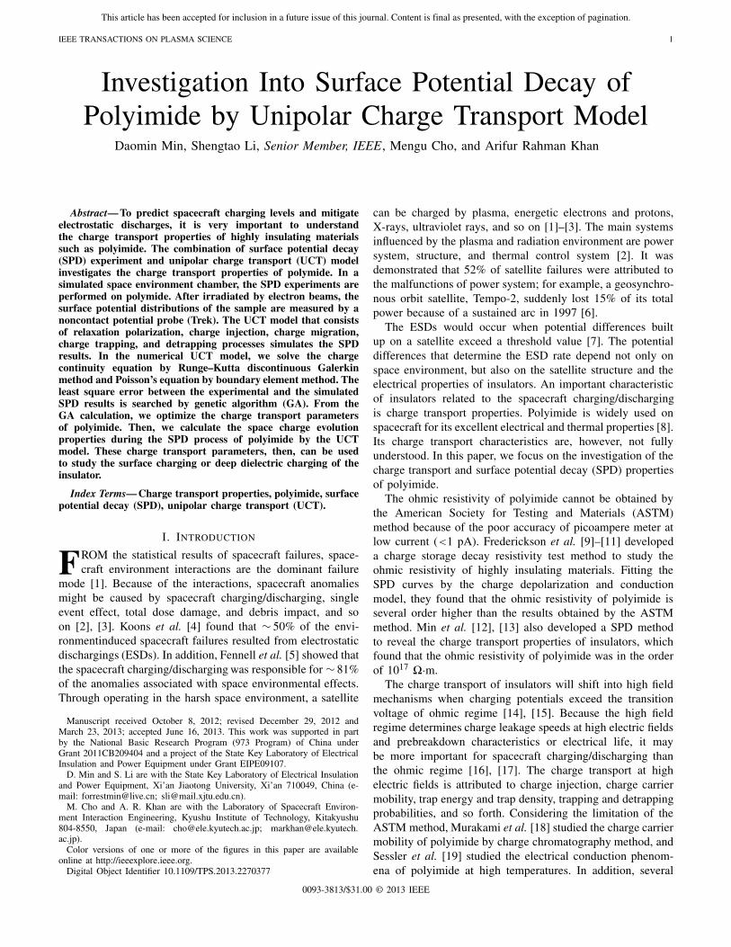
Fig. 1. Schematic view of charge injection into dielectrics and charge trappingand detrapping process in the energy band under electrical stresses. EeT isthe energy of deep traps and EF is the Fermi level (EF ≈ 3.5 eV [32]).
researchers have done some works on the trap density ofpolyimide by different methods, such as thermally simulatedcurrent (TSC) method, voltammetry, and so on [19]–[24].
The objective of this paper is to model the SPD processof polyimide irradiated by electron beams by a unipolarcharge transport (UCT) model with optimized charge transportparameters. The UCT model is described in detail in Section II,which includes charge release from surface traps, chargemigration through shallow traps, charge trapping/detrapping involume deep traps, and slow polarization processes. The exper-imental SPD results are shown in Section III. In Section IV,we optimize the charge transport parameters of polyimide andobtain the space charge evolution properties of the mater-ial with the optimized parameters at room temperature. InSection V, we conclude this paper with suggestion of worksto be done in the near future.
II. UCT MODEL
Charges will be accumulated on the surface of an insulatingmaterial and a surface potential will be built up when thematerial is irradiated by low energy (several keV) electronsfor a short time, as shown in Fig. 1. Once an electric fieldis established in the material, the deposited charges on thesurface will be accelerated to flow into the material. Some ofthe injected charges will drift through the shallow traps towardthe grounded electrode with an effective carrier mobility;some of them will be trapped by deep traps in the bulkwith a trapping probability. Deep trapped charges can bethermally released to the shallow traps with a detrappingprobability [25]. These charge transport processes of insulatorsare proved by experimental results by using space chargemapping techniques, such as pulsed electroacoustic (PEA)[26]–[28], laserinduced pressure pulse (LIPP) [29], [30], andpressure wave propagation [31].
Fig. 1 shows the schematic view of the whole processesin the energy band [33], [34]. The deposited electronslayer corresponds to the insulator surface and is defined asx = 0. The anode corresponds to the grounded electrode andis defined as x = L. The L is the thickness of the material.Electrons will be injected into and migrate in the upper half
energy band [28]. In the meantime, the surface potential willdecay in time [9], [11]. The SPD curves can be dividedinto different parts, which are resulted by different physicalprocesses, respectively. Therefore, the SPD characteristics ofinsulating materials can be used to reveal the charge trapping,detrapping, and conduction properties [34].
When the irradiation energy is relatively low, we assumethat the charges are just accumulated on the surface of thematerial. We also assume that few charges are injected insidethe material during a very short irradiation period with highirradiation current. We suppose that charge carriers are onlyinjected from the irradiated surface into the bulk of the mater-ial, and no carriers are provided by impurity ionization, field-induced dissociation or field-assisted generation. The currentdensity of electrons injected from the deposited electrons layerinto the bulk of the insulator is described by charge detrappingfrom the surface traps with Poole–Frenkel effect [35], [36]
jSe (0, t) = QS (t) × νATE × exp
(− EST − �EPF
kB · T
)(1)
where jSe is the electrons flowing from the surface chargelayer into the bulk of insulator in A·m−2, Qs(t) is the chargedensity on the irradiated surface in C·m−2, νATE is the attemptto escape frequency in s−1, and νATE = kB T /h p . kB is theBoltzmann constant, T is the temperature in K, h p is thePlanck constant, EST is the surface trap energy in eV and�EPF is the Poole–Frenkel effect
�EPF (t) = √qe · F (0, t) π · ε0 · εr (2)
where, qe is the elementary charge in C, ε0 is the dielectricpermittivity of vacuum in F/m, εr is the relative permittivity,and F(0, t) is the electric field at x = in V·m−1.
The charges in dielectrics obey the charge continuity law
∂qtotal (x, t)
∂ t+ ∂ jc (x, t)
∂x= S (x, t) (3)
where qtotal is the total electron density in the dielectric inC·m−3, jc is the conducting current density in the material inA·m−2, and S is the source term representing the local changein charge density, including charge trapping and detrapping.
The current density in the material via a constant shallowtrapcontrolled carrier mobility without regard to the chargediffusion can be interpreted by the conduction equation
jc (x, t) = qfree (x, t) · μ · F (x, t) (4)
where qfree is the free electron density in C·m−3, μ is thecharge carrier mobility in m2·V−1·s−1, and F is the electricfield in the material.
The charge source term or charge dynamics considerstwo species of carriers, namely, free, and trapped electrons.The free carriers can migrate in shallow traps, which areusually caused by physical or conformational defects. Chargetrapping and detrapping are described by considering sin-glelevel deep traps, which are caused by chemical defects [25]
Seμ = −Ptr · qfree · (1 − qtrap/Qtrap
) + Pde · qtrap (5)
Set = Ptr · qfree · (1 − qtrap/Qtrap
) − Pde · qtrap (6)
This article has been accepted for inclusion in a future issue of this journal. Content is final as presented, with the exception of pagination.
MIN et al.: INVESTIGATION INTO SURFACE POTENTIAL DECAY 3
where Seμ and Set are the charge sources of mobile and trappedelectrons, respectively, Ptr is the trapping coefficients of elec-trons in s−1, Pde is the detrapping coefficients of electrons ins−1, qtrap is the charge density of trapped electrons in C·m−3,and Qtrap is the trap density of electrons in C·m−3.
The detrapping coefficients for electrons in the bulk of theinsulator can be expressed as [34]
Pde = υATE · exp
(− EeT
kB · T
)(7)
where EeT is the deep trap energy for electrons in eV.Combining Poisson’s equation, we obtain a set of self-
consistent equations for UCT model
∂2φ (x, t)
∂x2 = −qtotal (x, t)
ε0εr(8)
where φ is the potential in the irradiated material in V.Finally, we can calculate the surface potential of the insu-
lator by integrating the electric field with the coordinate x
φS (t) =∫ L
0F (x, t) dx (9)
where φS(t) is the surface potential of the irradiated materialat time t in V.
We set the immediate shutdown of electron beam as thebeginning of SPD of the insulator, noted as t = 0 s. Conse-quently, the initial surface electron density and induced chargedensity on the grounded electrode are given by
QS (t) = −QG (t) = ε0 · εr (t) · φS (t)
L, t = 0 s (10)
where, QG is the induced charge density on the groundedelectrode in C·m−2.
We assume that the polarizations of polyimide include asmall part of relaxation polarization, which would be con-tributed by dipoles and space charges [37]
εr (t) = ε∞ + (εs − ε∞)[1 + (τ/t)(1−α) sin(πα/2)
]1 + 2 (τ/t)(1−α) sin(πα/2) + (τ/t)2(1−α)
(11)where ε∞ is the relative permittivity of instantaneous polar-ization, εs is the steadystate relative permittivity, and τand α are the relaxation time constant and relaxation timedistribution coefficient, respectively. The relative permittivityof instantaneous polarization, ε∞, is assumed as a constantvalue in this paper, which is ∼ 3.4 in the frequency range of10−1–103 Hz at room temperature measured by novocontrolbroadband dielectric spectroscopy (novocontrol) [38].
III. EXPERIMENTAL RESULTS
The SPD experiments of polyimide with the thickness of27 μm are performed in a vacuum chamber with the pressureof ∼ 5 × 10⁻⁴ Pa. The samples are irradiated by an electronbeam with the energy of 3 keV and the emission current of30 μA for ∼ 3 min. After irradiation, the 2-D surface potentialsof the samples are measured by a noncontact potential probe(Trek 341B) and recorded by a Labview program.
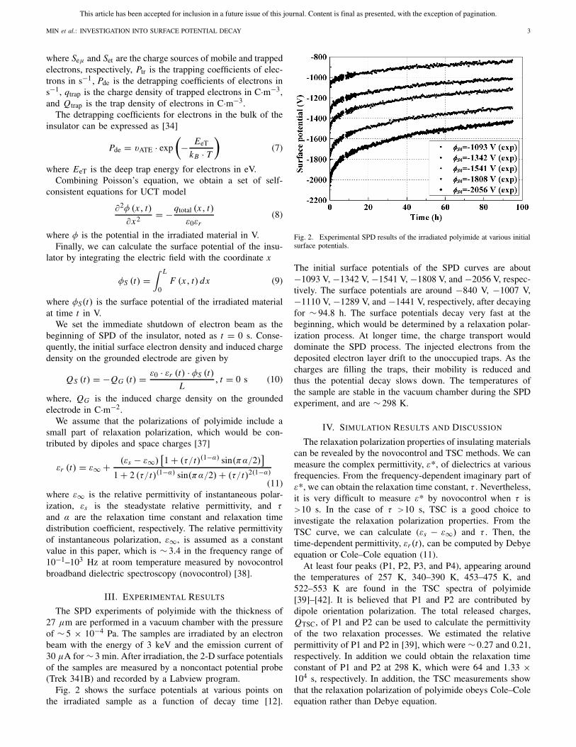
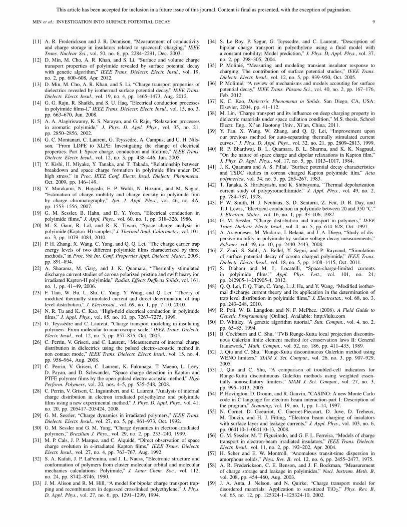
Fig. 2 shows the surface potentials at various points onthe irradiated sample as a function of decay time [12].
Fig. 2. Experimental SPD results of the irradiated polyimide at various initialsurface potentials.
The initial surface potentials of the SPD curves are about−1093 V, −1342 V, −1541 V, −1808 V, and −2056 V, respec-tively. The surface potentials are around −840 V, −1007 V,−1110 V, −1289 V, and −1441 V, respectively, after decayingfor ∼ 94.8 h. The surface potentials decay very fast at thebeginning, which would be determined by a relaxation polar-ization process. At longer time, the charge transport woulddominate the SPD process. The injected electrons from thedeposited electron layer drift to the unoccupied traps. As thecharges are filling the traps, their mobility is reduced andthus the potential decay slows down. The temperatures ofthe sample are stable in the vacuum chamber during the SPDexperiment, and are ∼ 298 K.
IV. SIMULATION RESULTS AND DISCUSSION
The relaxation polarization properties of insulating materialscan be revealed by the novocontrol and TSC methods. We canmeasure the complex permittivity, ε*, of dielectrics at variousfrequencies. From the frequency-dependent imaginary part ofε*, we can obtain the relaxation time constant, τ . Nevertheless,it is very difficult to measure ε* by novocontrol when τ is>10 s. In the case of τ >10 s, TSC is a good choice toinvestigate the relaxation polarization properties. From theTSC curve, we can calculate (εs − ε∞) and τ . Then, thetime-dependent permittivity, εr (t), can be computed by Debyeequation or Cole–Cole equation (11).
At least four peaks (P1, P2, P3, and P4), appearing aroundthe temperatures of 257 K, 340–390 K, 453–475 K, and522–553 K are found in the TSC spectra of polyimide[39]–[42]. It is believed that P1 and P2 are contributed bydipole orientation polarization. The total released charges,QTSC, of P1 and P2 can be used to calculate the permittivityof the two relaxation processes. We estimated the relativepermittivity of P1 and P2 in [39], which were ∼ 0.27 and 0.21,respectively. In addition we could obtain the relaxation timeconstant of P1 and P2 at 298 K, which were 64 and 1.33 ×10⁴ s, respectively. In addition, the TSC measurements showthat the relaxation polarization of polyimide obeys Cole–Coleequation rather than Debye equation.
This article has been accepted for inclusion in a future issue of this journal. Content is final as presented, with the exception of pagination.
4 IEEE TRANSACTIONS ON PLASMA SCIENCE
The TSC method can also be used to observe and analyzethe trap properties of insulating materials. Charge detrappingor injection processes can result in TSC peaks such as P3 andP4 in the TSC curves of polyimide [39]–[42]. It was foundthat the trap depths of polyimide are located in the range0.65–1.34 [23], [39]. Measuring the TSC spectra of coronacharged polyimide, Quamara et al. [41] found that the acti-vation energy of P4 (∼ 522 K) was ∼1.15 − 1.4 eV. Themeasurements show that the surface trap depth of pristinepolyimide is ∼ 1.4 eV.
As shown in Fig. 1, the charges released from the surfacetraps will migrate through the shallow traps to the rearelectrode. From (7), we can estimate that the residence timesof carriers are 7.92 × 10⁻¹² s and 1.34 × 10⁴ s at 298 K in thetrap depth of 0.1 and 1 eV, respectively. The carriers can hopin the shallow traps easily; however, will stay in the deep trapsfor very long times. In other words, the shallow traps can assistthe conduction process; however, the deep traps will controlthe space charge dynamics rather than the conduction [25].Consequently, the shallow traps will control the temperature-dependent hopping of mobile charges in the extended statesat relative low temperature. When the temperature increases,the residence time of carriers in a deep trap will reducedramatically, e.g. 0.648 s at 400 K in the trap depth of 1 eV.This means that the deep traps can also assist the conductionprocess at high temperatures. Many researchers found thatthe activation energy of charge transport increased with theincrease of temperature [19], [43]. Therefore, we just adopta single deep trap to simulate its influence on space chargeproperties at room temperature.
The carrier mobility of polyimide was investigated by LIPP[29], [44], SPD [19], [45], [46], space charge limited current(SCLC) [19], [47], and so on. It was found that the carriermobility of polyimide was in the range 2.06 × 10⁻¹⁷–3 ×10⁻¹⁵ m2·V−1·s−1. In addition, Sessler et al. [29], [30], [44]suggested that μ/Ptr could be assumed as a constant, andμ/Ptr was in the range from 3 × 10⁻¹⁵ to 6 × 10⁻¹³ m2·V−1
for polyimide. According to [46], we set μ ≈ 3.15 × 10⁻¹⁶
m2·V−1·s−1 and μ/Ptr ≈ 2.27 × 10⁻¹³ m2·V−1 in thefollowing simulations. In addition, the deeptrap density isassumed as 208 C·m−3 (or 1.3 × 10²¹ m−3) in this paper[13], [23], [48].
From the previous investigations, we can determine valuesor ranges of relaxation polarization and charge transport prop-erties of polyimide, as listed in Table I. We still have fourundetermined parameters in the UCT model. Because geneticalgorithm (GA) can optimize problems that have more thantwo unknowns [49], [50], we use the GA method to optimizethe four unknowns. The fitness function of GA is set as theleast square error between the experimental and the calculatedSPD results by UCT model
Error =
[∑tendt=0
[φUCT
s (t) − φExperiments (t)
]2]1 2
[∑tendt=0
(φ
Experiments (t)
)2]1/2 · 100%
(12)where tend is the total calculation time for GA.
TABLE I
INITIAL RANGES OF CHARGE TRANSPORT PARAMETERS OF POLYIMIDE
ESTIMATED FROM THE EXISTING FINDINGS
The nonlinear charge continuity equation (3) is numeri-cally solved by Runge–Kutta discontinuous Galerkin (RKDG)method [51]. The RKDG method consists of a third-orderexplicit Runge–Kutta time discretization and a finite elementspace discretization. The time discretization preserves nonlin-ear stability. The space discretization incorporates an approx-imate Riemann solver (or numerical flux) and a slope limiter.Because of the nonlinear nature of the charge continuityequation, the high-order accurate RKDG scheme generatesspurious oscillations around the discontinuities. The stabilityof RKDG method requires to be enforced by slope or fluxlimiters [51]. A weighted essentially nonoscillatory limiter isused in this paper [52], [53].
The sample of polyimide is divided into 200 parts in theUCT simulation (�x = 0.135 μm). The interval time, �t ,is set as 1 s in the simulation, which satisfy the Courant–Friedrich–Levy restriction (μ · F)max ≤ �x /�t [51]. The totalcalculation time is 95 h.
A. Comparisons of Experimental and Calculated SPDs
Calculating by the UCT model with GA, we optimizethe charge transport properties of polyimide, as shown inTable II. The GA simulations are all iterated >900 times atthe five initial surface potentials. The best fitness errors ofthe GA programs are all < 0.28% at various initial surfacepotentials. Figs. 3 and 4 show the SPD curves simulated byUCT model with the charge transport parameters in Table IIin linear and semilogarithmic coordinates, respectively. Fromthe comparisons of the experimental and the calculated SPDresults, it is clear that the two SPD results are in goodagreement with each other.
The surface trap energies of polyimide are in the rangefrom 1.310 to 1.383 eV, at the initial surface potentialsfrom −1093 to −2056 V. The surface trap energy goes upwith increasing the initial surface potential. It shows thatthe electron beam irradiation processes affect the detrappingproperties of surface charges. Definitely, the incident electronscan penetrate into the insulating material with a small range.Consequently, the electrons are distributed in the penetrationdirection. The electron distribution will establish an electricfield distribution in the material. Analyzing by Poisson’s

This article has been accepted for inclusion in a future issue of this journal. Content is final as presented, with the exception of pagination.
MIN et al.: INVESTIGATION INTO SURFACE POTENTIAL DECAY 5
TABLE II
CHARGE TRANSPORT PARAMETERS OF POLYIMIDE OBTAINED BY THE
COMBINATION OF UCT MODEL AND GA METHOD AT VARIOUS
INITIAL SURFACE POTENTIALS
Fig. 3. Experimental and calculated SPD results of the irradiated insulatorat various initial surface potentials in linear coordinates.
equation, we acknowledge that the electric field decreases fromthe penetration range to x = 0. Because the Poole–Frenkeleffect �EPF is directly proportional to F1/2, �EPF woulddescend from the penetration range to x = 0, too. Accordingly,the optimized surface trap depths will vary when the electrondistributions caused by irradiation are different.
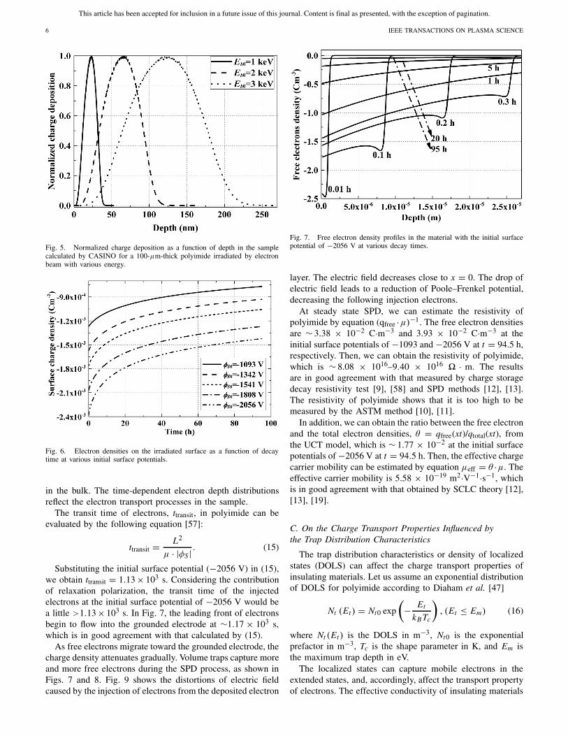
The penetration range of electrons in polyimide as a func-tion of incident energy can be calculated by Monte Carlosimulation of electron trajectory in solid (CASINO) [54].Fig. 5 shows the normalized charge density as a function ofdepth in the sample calculated by CASINO for a 100-μm-thickpolyimide film deposited by electron beam with the energiesin the range from 1 to 3 keV [54]. The number of simulatedelectrons is 2 × 10⁷. The results show that the incident chargeparticles with higher energy can penetrate deeper into the bulkof the material. For example, the penetration ranges of incidentenergy of 1 and 3 keV are 0.044 and 0.266 μm, respectively.
As the electrons being accumulated in the material dur-ing irradiation, potentials will be built up on the surface.Then, the electrons energy landing on the surface will bereduced, which can be estimated by the following equation[55]:
Eb (t) = Eb0 − qeφS (t) (13)
Fig. 4. Experimental and calculated SPD results of the irradiated insulatorat various initial surface potentials in semilogarithmic coordinates.
where Eb(t) is the electron beam energy landing on the sampleat time t in eV and Eb is the electron beam energy at t = 0 s.
When the income electrons equal to the outcome electronsconsist of backscatter and secondary emission electrons, thesurface potential of the material reaches equilibrium. The cen-troid of the deposited electrons can be calculated by [29]
Xc =∫ R(Eb)
0 xqtotal (x) dx∫ R(Eb)0 qtotal (x) dx
(14)
where Xc is the centroid of deposited electrons in m andR(Eb) is the penetration range of electrons with the energyof Eb.
Sessler et al. [56] found that the centroids of depositedelectrons in insulating materials were directly proportionalto the injected charge density. Accordingly, the centroid ofdeposited electrons at higher initial surface potential wouldbe larger than that at lower initial surface potential. It showsthat the higher initial surface potential has stronger influenceon the Poole–Frenkel effect. Therefore, the optimized surfacetrap energy is deeper at higher initial surface potential.
B. Space Charge Evolution During SPD
More details about the charge retention on the surface andcharge propagation in the bulk of the insulator can be obtainedby substituting the charge transport parameters in Table II intothe UCT model. Fig. 6 shows that the electron densities onthe surface decrease gradually. The electron density depositedon the irradiated surface with the initial surface potentialof −2056 V is 2.36 × 10⁻³ C·m−2, estimated by (10).39.72% of the surface electrons are released from the surfacetrap centers to the bulk in 94.8 h, which interprets that theretention time of deposited electrons is very long for polyimide[27], [44].
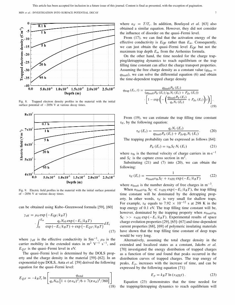
Figs. 7 and 8 show the free electron density and trappedelectron density profiles at various decay times, which are con-sistent with the experimental results measured by space chargemapping techniques [27], [44]. Homocharges are accumulated
This article has been accepted for inclusion in a future issue of this journal. Content is final as presented, with the exception of pagination.
6 IEEE TRANSACTIONS ON PLASMA SCIENCE
Fig. 5. Normalized charge deposition as a function of depth in the samplecalculated by CASINO for a 100-μm-thick polyimide irradiated by electronbeam with various energy.
Fig. 6. Electron densities on the irradiated surface as a function of decaytime at various initial surface potentials.
in the bulk. The time-dependent electron depth distributionsreflect the electron transport processes in the sample.
The transit time of electrons, ttransit, in polyimide can beevaluated by the following equation [57]:
ttransit = L2
μ · |φS | . (15)
Substituting the initial surface potential (−2056 V) in (15),we obtain ttransit = 1.13 × 10³ s. Considering the contributionof relaxation polarization, the transit time of the injectedelectrons at the initial surface potential of −2056 V would bea little >1.13 × 10³ s. In Fig. 7, the leading front of electronsbegin to flow into the grounded electrode at ∼1.17 × 10³ s,which is in good agreement with that calculated by (15).
As free electrons migrate toward the grounded electrode, thecharge density attenuates gradually. Volume traps capture moreand more free electrons during the SPD process, as shown inFigs. 7 and 8. Fig. 9 shows the distortions of electric fieldcaused by the injection of electrons from the deposited electron
Fig. 7. Free electron density profiles in the material with the initial surfacepotential of −2056 V at various decay times.
layer. The electric field decreases close to x = 0. The drop ofelectric field leads to a reduction of Poole–Frenkel potential,decreasing the following injection electrons.
At steady state SPD, we can estimate the resistivity ofpolyimide by equation (qfree ·μ)−1. The free electron densitiesare ∼ 3.38 × 10⁻² C·m−3 and 3.93 × 10⁻² C·m−3 at theinitial surface potentials of −1093 and −2056 V at t = 94.5 h,respectively. Then, we can obtain the resistivity of polyimide,which is ∼ 8.08 × 10¹⁶–9.40 × 10¹⁶ � · m. The resultsare in good agreement with that measured by charge storagedecay resistivity test [9], [58] and SPD methods [12], [13].The resistivity of polyimide shows that it is too high to bemeasured by the ASTM method [10], [11].
In addition, we can obtain the ratio between the free electronand the total electron densities, θ = qfree(xt)/qtotal(xt), fromthe UCT model, which is ∼ 1.77 × 10⁻² at the initial surfacepotentials of −2056 V at t = 94.5 h. Then, the effective chargecarrier mobility can be estimated by equation μeff = θ ·μ. Theeffective carrier mobility is 5.58 × 10⁻¹⁹ m2·V−1·s−1, whichis in good agreement with that obtained by SCLC theory [12],[13], [19].
C. On the Charge Transport Properties Influenced bythe Trap Distribution Characteristics
The trap distribution characteristics or density of localizedstates (DOLS) can affect the charge transport properties ofinsulating materials. Let us assume an exponential distributionof DOLS for polyimide according to Diaham et al. [47]
Nt (Et ) = Nt0 exp
(− Et
kB Tc
), (Et ≤ Em) (16)
where Nt (Et ) is the DOLS in m−3, Nt0 is the exponentialprefactor in m−3, Tc is the shape parameter in K, and Em isthe maximum trap depth in eV.
The localized states can capture mobile electrons in theextended states, and, accordingly, affect the transport propertyof electrons. The effective conductivity of insulating materials
This article has been accepted for inclusion in a future issue of this journal. Content is final as presented, with the exception of pagination.
MIN et al.: INVESTIGATION INTO SURFACE POTENTIAL DECAY 7
Fig. 8. Trapped electron density profiles in the material with the initialsurface potential of −2056 V at various decay times.
Fig. 9. Electric field profiles in the material with the initial surface potentialof −2056 V at various decay times.
can be obtained using Kubo–Greenwood formula [59], [60]
γeff = μ0 exp(−EQF/kB T
)
·∫ Em
0
qe Nt0 exp (−Et/kB T )
exp (−Et/kB T ) + exp(−EQ F/kB T
)d Et
(17)
where γeff is the effective conductivity in Sm−1, μ0 is thecarrier mobility in the extended states in m2 V−1 s−1, andEQ F is the quasi–Fermi level in eV.
The quasi–Fermi level is determined by the DOLS prop-erty and the charge density in the material [59]–[62]. In anexponential-type DOLS, Anta et al. [59] derived the followingequation for the quasi–Fermi level:
EQ F = −kB Tc ln
[qtotal
qe Nt0[1 + (παd )2/6 + 7(παd )4/360
]]
(18)
where αd = T /Tc. In addition, Boufayed et al. [63] alsoobtained a similar equation. However, they did not considerthe influence of disorder on the quasi–Fermi level.
From (17), we can find that the activation energy of theeffective conductivity is EQF rather than Em . Consequently,we can just obtain the quasi–Fermi level EQF but not themaximum trap depth Em from the Arrhenius formula.
On the other hand, the time needed for the charge trap-ping/detrapping dynamics to reach equilibrium or the trapfilling time constant can affect the charge transport properties.Assuming the free charge density as a constant value (qfree =qfree0), we can solve the differential equation (6) and obtainthe time-dependent trapped charge density
qtrap (Et , t) = qfree0 Ptr (Et )
(qfree0 Ptr (Et )/qe Nt (Et ) + Pde (Et ))
·[
1 − exp
(−
(qfree0 Ptr (Et )
qe Nt (Et )+ Pde (Et )
)t
)].
(19)
From (19), we can estimate the trap filling time constantτtf , by the following equation:
τtf (Et ) = qe Nt (Et )
qfree0 Ptr (Et ) + Pdeqe Nt (Et ). (20)
The trapping probability can be expressed as follows [64]:
Ptr (Et ) = νth SC Nt (Et ) (21)
where vth is the thermal velocity of charge carriers in m·s−1
and SC is the capture cross section in m2.Substituting (21) and (7) into (20), we can obtain the
following:
τtf (Et ) = 1
nfree0νth SC + υATE exp (−Et/kB T )(22)
where nfree0 is the number density of free charges in m−3.When nfree0νth SC � υATE exp (−Et/kB T ), the trap filling
time constant will be dominated by the detrapping prop-erty. In other words, τtf is very small for shallow traps.For example, τtf equals to 7.92 × 10⁻¹² s at 298 K in thetrap energy of 0.1 eV. The trap filling time constant will be,however, dominated by the trapping property when nfree0νthSC >> υATE exp (−Et/kB T ). Experimental results of spacecharge evolution properties [29], [65]–[67] and time-dependentcurrent properties [68], [69] of polymeric insulating materialshave shown that the trap filling time constant of deep trapswould be very long.
Alternatively, assuming the total charge density in theextended and localized states as a constant, Jakobs et al.[70] investigated the energy distribution of trapped chargesas a function of time and found that peaks occurred in thedistribution curves of trapped charges. The trap energy ofpeaks, E p, increases with the increase of time, and can beexpressed by the following equation [71]:
E p = kB T ln (υATEt) . (23)
Equation (23) demonstrates that the time needed forthe trapping/detrapping dynamics to reach equilibrium will
This article has been accepted for inclusion in a future issue of this journal. Content is final as presented, with the exception of pagination.
8 IEEE TRANSACTIONS ON PLASMA SCIENCE
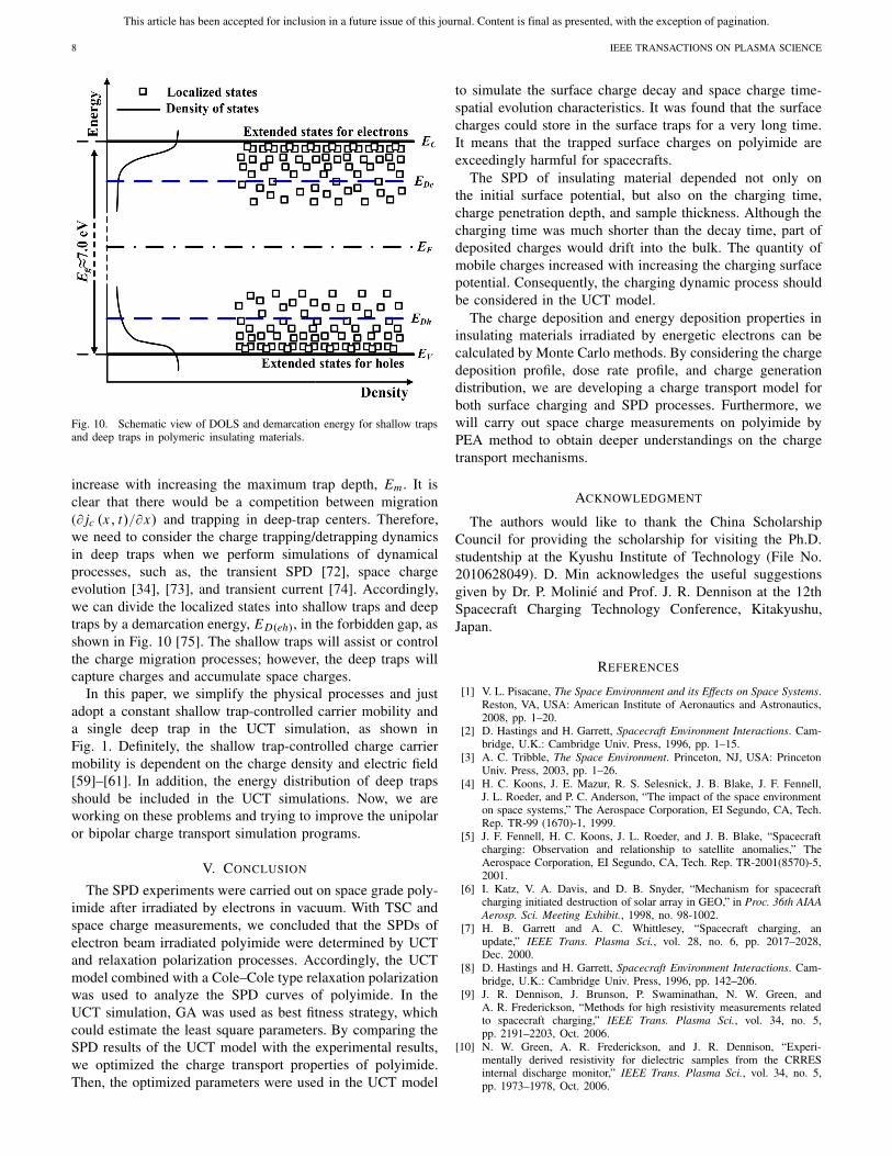
Fig. 10. Schematic view of DOLS and demarcation energy for shallow trapsand deep traps in polymeric insulating materials.
increase with increasing the maximum trap depth, Em . It isclear that there would be a competition between migration(∂ jc (x, t)/∂x) and trapping in deep-trap centers. Therefore,we need to consider the charge trapping/detrapping dynamicsin deep traps when we perform simulations of dynamicalprocesses, such as, the transient SPD [72], space chargeevolution [34], [73], and transient current [74]. Accordingly,we can divide the localized states into shallow traps and deeptraps by a demarcation energy, ED(eh), in the forbidden gap, asshown in Fig. 10 [75]. The shallow traps will assist or controlthe charge migration processes; however, the deep traps willcapture charges and accumulate space charges.
In this paper, we simplify the physical processes and justadopt a constant shallow trap-controlled carrier mobility anda single deep trap in the UCT simulation, as shown inFig. 1. Definitely, the shallow trap-controlled charge carriermobility is dependent on the charge density and electric field[59]–[61]. In addition, the energy distribution of deep trapsshould be included in the UCT simulations. Now, we areworking on these problems and trying to improve the unipolaror bipolar charge transport simulation programs.
V. CONCLUSION
The SPD experiments were carried out on space grade poly-imide after irradiated by electrons in vacuum. With TSC andspace charge measurements, we concluded that the SPDs ofelectron beam irradiated polyimide were determined by UCTand relaxation polarization processes. Accordingly, the UCTmodel combined with a Cole–Cole type relaxation polarizationwas used to analyze the SPD curves of polyimide. In theUCT simulation, GA was used as best fitness strategy, whichcould estimate the least square parameters. By comparing theSPD results of the UCT model with the experimental results,we optimized the charge transport properties of polyimide.Then, the optimized parameters were used in the UCT model
to simulate the surface charge decay and space charge time-spatial evolution characteristics. It was found that the surfacecharges could store in the surface traps for a very long time.It means that the trapped surface charges on polyimide areexceedingly harmful for spacecrafts.
The SPD of insulating material depended not only onthe initial surface potential, but also on the charging time,charge penetration depth, and sample thickness. Although thecharging time was much shorter than the decay time, part ofdeposited charges would drift into the bulk. The quantity ofmobile charges increased with increasing the charging surfacepotential. Consequently, the charging dynamic process shouldbe considered in the UCT model.
The charge deposition and energy deposition properties ininsulating materials irradiated by energetic electrons can becalculated by Monte Carlo methods. By considering the chargedeposition profile, dose rate profile, and charge generationdistribution, we are developing a charge transport model forboth surface charging and SPD processes. Furthermore, wewill carry out space charge measurements on polyimide byPEA method to obtain deeper understandings on the chargetransport mechanisms.
ACKNOWLEDGMENT
The authors would like to thank the China ScholarshipCouncil for providing the scholarship for visiting the Ph.D.studentship at the Kyushu Institute of Technology (File No.2010628049). D. Min acknowledges the useful suggestionsgiven by Dr. P. Molinié and Prof. J. R. Dennison at the 12thSpacecraft Charging Technology Conference, Kitakyushu,Japan.
REFERENCES
[1] V. L. Pisacane, The Space Environment and its Effects on Space Systems.Reston, VA, USA: American Institute of Aeronautics and Astronautics,2008, pp. 1–20.
[2] D. Hastings and H. Garrett, Spacecraft Environment Interactions. Cam-bridge, U.K.: Cambridge Univ. Press, 1996, pp. 1–15.
[3] A. C. Tribble, The Space Environment. Princeton, NJ, USA: PrincetonUniv. Press, 2003, pp. 1–26.
[4] H. C. Koons, J. E. Mazur, R. S. Selesnick, J. B. Blake, J. F. Fennell,J. L. Roeder, and P. C. Anderson, “The impact of the space environmenton space systems,” The Aerospace Corporation, EI Segundo, CA, Tech.Rep. TR-99 (1670)-1, 1999.
[5] J. F. Fennell, H. C. Koons, J. L. Roeder, and J. B. Blake, “Spacecraftcharging: Observation and relationship to satellite anomalies,” TheAerospace Corporation, EI Segundo, CA, Tech. Rep. TR-2001(8570)-5,2001.
[6] I. Katz, V. A. Davis, and D. B. Snyder, “Mechanism for spacecraftcharging initiated destruction of solar array in GEO,” in Proc. 36th AIAAAerosp. Sci. Meeting Exhibit., 1998, no. 98-1002.
[7] H. B. Garrett and A. C. Whittlesey, “Spacecraft charging, anupdate,” IEEE Trans. Plasma Sci., vol. 28, no. 6, pp. 2017–2028,Dec. 2000.
[8] D. Hastings and H. Garrett, Spacecraft Environment Interactions. Cam-bridge, U.K.: Cambridge Univ. Press, 1996, pp. 142–206.
[9] J. R. Dennison, J. Brunson, P. Swaminathan, N. W. Green, andA. R. Frederickson, “Methods for high resistivity measurements relatedto spacecraft charging,” IEEE Trans. Plasma Sci., vol. 34, no. 5,pp. 2191–2203, Oct. 2006.
[10] N. W. Green, A. R. Frederickson, and J. R. Dennison, “Experi-mentally derived resistivity for dielectric samples from the CRRESinternal discharge monitor,” IEEE Trans. Plasma Sci., vol. 34, no. 5,pp. 1973–1978, Oct. 2006.
This article has been accepted for inclusion in a future issue of this journal. Content is final as presented, with the exception of pagination.
MIN et al.: INVESTIGATION INTO SURFACE POTENTIAL DECAY 9
[11] A. R. Frederickson and J. R. Dennison, “Measurement of conductivityand charge storage in insulators related to spacecraft charging,” IEEETrans. Nuclear Sci., vol. 50, no. 6, pp. 2284–2291, Dec. 2003.
[12] D. Min, M. Cho, A. R. Khan, and S. Li, “Surface and volume chargetransport properties of polyimide revealed by surface potential decaywith genetic algorithm,” IEEE Trans. Dielectr. Electr. Insul., vol. 19,no. 2, pp. 600–608, Apr. 2012.
[13] D. Min, M. Cho, A. R. Khan, and S. Li, “Charge transport properties ofdielectrics revealed by isothermal surface potential decay,” IEEE Trans.Dielectr. Electr. Insul., vol. 19, no. 4, pp. 1465–1473, Aug. 2012.
[14] G. G. Raju, R. Shaikh, and S. U. Haq, “Electrical conduction processesin polyimide films-I,” IEEE Trans. Dielectr. Electr. Insul., vol. 15, no. 3,pp. 663–670, Jun. 2008.
[15] A. A. Alagiriswamy, K. S. Narayan, and G. Raju, “Relaxation processesin aromatic polyimide,” J. Phys. D. Appl. Phys., vol. 35, no. 21,pp. 2850–2856, 2002.
[16] G. C. Montanari, C. Laurent, G. Teyssedre, A. Campus, and U. H. Nils-son, “From LDPE to XLPE: Investigating the change of electricalproperties. Part I: Space charge, conduction and lifetime,” IEEE Trans.Dielectr. Electr. Insul., vol. 12, no. 3, pp. 438–446, Jun. 2005.
[17] Y. Kishi, H. Miyake, Y. Tanaka, and T. Takada, “Relationship betweenbreakdown and space charge formation in polyimide film under DChigh stress,” in Proc. IEEE Conf. Electr. Insul. Dielectr. Phenomena,Oct. 2009, pp. 146–149.
[18] Y. Murakami, N. Hayashi, E. P. Waldi, N. Hozumi, and M. Nagao,“Estimation of charge mobility and charge density in polyimide filmby charge chromatography,” Jpn. J. Appl. Phys., vol. 46, no. 4A,pp. 1553–1556, 2007.
[19] G. M. Sessler, B. Hahn, and D. Y. Yoon, “Electrical conduction inpolyimide films,” J. Appl. Phys., vol. 60, no. 1, pp. 318–326, 1986.
[20] M. S. Gaur, R. Lal, and R. K. Tiwari, “Space charge analysis inpolyimide (Kapton–H) samples,” J. Thermal Anal. Calorimetry, vol. 101,no. 3, pp. 1079–1084, 2010.
[21] P. H. Zhang, X. Wang, C. Yang, and Q. Q. Lei, “The charge carrier trapenergy levels of two different polyimide films characterized by threemethods,” in Proc. 9th Int. Conf. Properties Appl. Dielectr. Mater., 2009,pp. 891–894.
[22] A. Sharama, M. Garg, and J. K. Quamara, “Thermally stimulateddischarge current studies of corona polarized pristine and swift heavy ionirradiated Kapton-H polyimide,” Radiat. Effects Deffects Solids, vol. 161,no. 1, pp. 41–49, 2006.
[23] F. Tian, W. Bu, L. Shi, C. Yang, Y. Wang, and Q. Lei, “Theory ofmodified thermally stimulated current and direct determination of traplevel distribution,” J. Electrostat., vol. 69, no. 1, pp. 7–10, 2010.
[24] N. R. Tu and K. C. Kao, “High-field electrical conduction in polyimidefilms,” J. Appl. Phys., vol. 85, no. 10, pp. 7267–7275, 1999.
[25] G. Teyssèdre and C. Laurent, “Charge transport modeling in insulatingpolymers: From molecular to macroscopic scale,” IEEE Trans. Dielectr.Electr. Insul., vol. 12, no. 5, pp. 857–875, Oct. 2005.
[26] C. Perrin, V. Griseri, and C. Laurent, “Measurement of internal chargedistribution in dielectrics using the pulsed electro-acoustic method innon contact mode,” IEEE Trans. Dielectr. Electr. Insul., vol. 15, no. 4,pp. 958–964, Aug. 2008.
[27] C. Perrin, V. Griseri, C. Laurent, K. Fukunaga, T. Maeno, L. Levy,D. Payan, and D. Schwander, “Space charge detection in Kapton andPTFE polymer films by the open pulsed electro-acoustic method,” HighPerform. Polymers, vol. 20, nos. 4–5, pp. 535–548, 2008.
[28] C. Perrin, V. Griseri, C. Inguimbert, and C. Laurent, “Analysis of internalcharge distribution in electron irradiated polyethylene and polyimidefilms using a new experimental method,” J. Phys. D, Appl. Phys., vol. 41,no. 20, pp. 205417–205424, 2008.
[29] G. M. Sessler, “Charge dynamics in irradiated polymers,” IEEE Trans.Dielectr. Electr. Insul., vol. 27, no. 5, pp. 961–973, Oct. 1992.
[30] G. M. Sessler and G. M. Yang, “Charge dynamics in electron-irradiatedpolymers,” Brazilian J. Phys., vol. 29, no. 2, pp. 233–240, 1999.
[31] M. P. Cals, J. P. Marque, and C. Alquidé, “Direct observation of spacecharge evolution in e-irradiated Kapton films,” IEEE Trans. Dielectr.Electr. Insul., vol. 27, no. 4, pp. 763–767, Aug. 1992.
[32] S. A. Kafafi, J. P. LaFemina, and J. L. Nauss, “Electronic structure andconformation of polymers from cluster molecular orbital and molecularmechanics calculations: Polyimide,” J. Amer Chem. Soc., vol. 112,no. 24, pp. 8742–8746, 1990.
[33] J. M. Alison and R. M. Hill, “A model for bipolar charge transport trap-ping and recombination in degassed crosslinked polyethylene,” J. Phys.D, Appl. Phys., vol. 27, no. 6, pp. 1291–1299, 1994.
[34] S. Le Roy, P. Segur, G. Teyssedre, and C. Laurent, “Description ofbipolar charge transport in polyethylene using a fluid model witha constant mobility: Model prediction,” J. Phys. D, Appl. Phys., vol. 37,no. 2, pp. 298–305, 2004.
[35] P. Molinié, “Measuring and modeling transient insulator response tocharging: The contribution of surface potential studies,” IEEE Trans.Dielectr. Electr. Insul., vol. 12, no. 5, pp. 939–950, Oct. 2005.
[36] P. Molimié, “A review of mechanisms and models accouting for surfacepotential decay,” IEEE Trans. Plasma Sci., vol. 40, no. 2, pp. 167–176,Feb. 2012.
[37] K. C. Kao, Dielectric Phenomena in Solids. San Diego, CA, USA:Elsevier, 2004, pp. 41–112.
[38] M. Lin, “Charge transport and its influence on deep charging property indielectric materials under space radiation condition,” M.S. thesis, SchoolElectr. Eng., Xi’an Jiaotong Univ., Xi’an, China, 2011.
[39] Y. Fan, X. Wang, W. Zhang, and Q. Q. Lei, “Improvement uponour previous method for auto-separating thermally stimulated currentcurves,” J. Phys. D, Appl. Phys., vol. 32, no. 21, pp. 2809–2813, 1999.
[40] R. P. Bhardwaj, B. L. Quamara, B. L. Sharma, and K. K. Nagpaul,“On the nature of space charge and dipolar relaxations in Kapton film,”J. Phys. D, Appl. Phys., vol. 17, no. 5, pp. 1013–1017, 1984.
[41] J. K. Quamara and A. S. Pillai, “Surface potential decay characteristicsand TSDC studies in corona charged Kapton polyimide film,” Actapolymerica, vol. 34, no. 5, pp. 265–267, 1983.
[42] T. Tanaka, S. Hirabayashi, and K. Shibayama, “Thermal depolarizationcurrent study of polypyromellitimide,” J. Appl. Phys., vol. 49, no. 2,pp. 784–787, 1978.
[43] F. W. Smith, H. J. Neuhaus, S. D. Senturia, Z. Feit, D. R. Day, andT. J. Lewis, “Electrical conduction in polyimide between 20 and 350 °C,”J. Electron. Mater., vol. 16, no. 1, pp. 93–106, 1987.
[44] G. M. Sessler, “Charge distribution and transport in polymers,” IEEETrans. Dielectr. Electr. Insul., vol. 4, no. 5, pp. 614–628, Oct. 1997.
[45] A. Aragoneses, M. Mudarra, J. Belana, and J. A. Diego, “Study of dis-persive mobility in polyimide by surface voltage decay measurements,”Polymer, vol. 49, no. 10, pp. 2440–2443, 2008.
[46] Z. Ziari, S. Sahli, A. Bellel, Y. Segui, and P. Raynaud, “Simulationof surface potential decay of corona charged polyimide,” IEEE Trans.Dielectr. Electr. Insul., vol. 18, no. 5, pp. 1408–1415, Oct. 2011.
[47] S. Diaham and M. L. Locatelli, “Space-charge-limited currentsin polyimide films,” Appl. Phys. Lett., vol. 101, no. 24,pp. 242905-1–242905-4, 2012.
[48] Q. Q. Lei, F. Q. Tian, C. Yang, L. J. He, and Y. Wang, “Modified isother-mal discharge current theory and its application in the determination oftrap level distribution in polyimide films,” J. Electrostat., vol. 68, no. 3,pp. 243–248, 2010.
[49] R. Poli, W. B. Langdon, and N. F. McPhee. (2008). A Field Guide toGenetic Programming [Online]. Available: http://lulu.com
[50] D. Whitley, “A genetic algorithm tutorial,” Stat. Comput., vol. 4, no. 2,pp. 65–85, 1994.
[51] B. Cockburn and C. Shu, “TVB Runge-Kutta local projection discontin-uous Galerkin finite element method for conservation laws II: Generalframework,” Math. Comput., vol. 52, no. 186, pp. 411–435, 1989.
[52] J. Qiu and C. Shu, “Runge-Kutta discontinuous Galerkin method usingWENO limiters,” SIAM J. Sci. Comput., vol. 26, no. 3, pp. 907–929,2005.
[53] J. Qiu and C. Shu, “A comparison of troubled-cell indicators forRunge-Kutta discontinuous Galerkin methods using weighted essen-tially nonoscillatory limiters,” SIAM J. Sci. Comput., vol. 27, no. 3,pp. 995–1013, 2005.
[54] P. Hovington, D. Drouin, and R. Gauvin, “CASINO: A new Monte Carlocode in C language for electron beam interaction-part I: Description ofthe program,” Scanning, vol. 19, no. 1, pp. 1–14, 1997.
[55] N. Cornet, D. Goeuriot, C. Guerret-Piecourt, D. Juve, D. Treheux,M. Touzin, and H. J. Fitting, “Electron beam charging of insulatorswith surface layer and leakage currents,” J. Appl. Phys., vol. 103, no. 6,pp. 064110-1–064110-13, 2008.
[56] G. M. Sessler, M. T. Figueiredo, and G. F. L. Ferreira, “Models of chargetransport in electron-beam irradiated insulators,” IEEE Trans. Dielectr.Electr. Insul., vol. 11, no. 2, pp. 192–202, Apr. 2004.
[57] H. Scher and E. W. Montroll, “Anomalous transit-time dispersion inamorphous solids,” Phys. Rev. B, vol. 12, no. 6, pp. 2455–2477, 1975.
[58] A. R. Frederickson, C. E. Benson, and J. F. Bockman, “Measurementof charge storage and leakage in polyimides,” Nucl. Instrum. Meth. B,vol. 208, pp. 454–460, Aug. 2003.
[59] J. A. Anta, J. Nelson, and N. Quirke, “Charge transport model fordisordered materials: Application to sensitized TiO2,” Phys. Rev. B,vol. 65, no. 12, pp. 125324-1–125324-10, 2002.
This article has been accepted for inclusion in a future issue of this journal. Content is final as presented, with the exception of pagination.
10 IEEE TRANSACTIONS ON PLASMA SCIENCE
[60] J. A. Anta, G. Marcelli, M. Meunier, and N. Quirke, “Models of electrontrapping and transport in polyethylene: Current-voltage characteristics,”J. Appl. Phys., vol. 92, no. 2, pp. 1002–1008, 2002.
[61] W. F. Pasveer, J. Cottaar, C. Tanase, R. Coehoorn, P. A. Bobbert,P. W. M. Blom, D. M. DeLeeuw, and M. A. J. Michels, “Unifieddescription of charge-carrier mobilities in disordered semiconductingpolymers,” Phys. Rev. Lett., vol. 94, no. 20, pp. 206601-1–206601-4,2005.
[62] C. Tanase, E. J. Meijer, P. W. M. Blom, and D. M. de Leeuw,“Unification of the hole transport in polymeric field-effect transis-tors and light-emitting diodes,” Phys. Rev. Lett., vol. 91, no. 21,pp. 216601-1–216601-4, 2003.
[63] F. Boufayed, G. Teyssedre, C. Laurent, S. Le Roy, L. A. Dissado,P. Segur, and G. C. Montanari, “Models of bipolar charge transport inpolyethylene,” J. Appl. Phys., vol. 100, no. 10, pp. 104105-1–104105-10,2006.
[64] J. G. Simmons and G. W. Taylor, “Nonequilibrium steady-state statisticsand associated effects for insulators and semiconductors containing anarbitrary distribution of traps,” Phys. Rev. B, vol. 4, no. 2, pp. 502–511,1971.
[65] T. Mizutani, H. Semi, and K. Kaneko, “Space charge behavior in low-density polyethylene,” IEEE Trans. Dielectr. Electr. Insul., vol. 7, no. 4,pp. 503–508, Aug. 2000.
[66] S. Le Roy, F. Baudoin, V. Griseri, C. Laurent, and G. Teyssedre,“Charge transport modelling in electron-beam irradiated dielectrics:A model for polyethylene,” J. Phys. D, Appl. Phys., vol. 43, no. 31,pp. 315402–315411, 2010.
[67] S. Le Roy, F. Baudoin, V. Griseri, C. Laurent, and G. Teyssedre,“Space charge modeling in electron-beam irradiated polyethylene:Fitting model and experiments,” J. Appl. Phys., vol. 112, no. 2,pp. 023704-1–023704-8, 2012.
[68] G. C. Montanari, G. Mazzanti, F. Palmieri, A. Motori, G. Perego, andS. Serra, “Space-charge trapping and conduction in LDPE, HDPE andXLPE,” J. Phys. D, Appl. Phys., vol. 34, no. 18, pp. 2902–2911, 2001.
[69] C. Guillermin, P. Rain, and S. W. Rowe, “Transient and steady-statecurrents in epoxy resin,” J. Phys. D, Appl. Phys., vol. 39, no. 3,pp. 515–524, 2006.
[70] A. Jakobs and K. W. Kehr, “Theory and simulation of multiple-trapping transport through a finite slab,” Phys. Rev. B, vol. 48, no. 12,pp. 8780–8789, 1993.
[71] J. Orenstein and M. Kastner, “Photocurrent transient spectroscopy:Measurement of the density of localized states in a-As2Se3,” Phys. Rev.Lett., vol. 46, no. 21, pp. 1421–1424, 1981.
[72] G. Chen, “A new model for surface potential decay of corona-charged polymers,” J. Phys. D, Appl. Phys., vol. 43, no. 5,pp. 055405-1–055405-7, 2010.
[73] J. H. Tian, J. Zou, Y. S. Wang, J. Liu, J. S. Yuan, and Y. X. Zhou,“Simulation of bipolar charge transport with trapping and recom-bination in polymeric insulators using Runge-Kutta discontinuousGalerkin method,” J. Phys. D, Appl. Phys., vol. 41, no. 19,pp. 195416-1–195416-10, 2008.
[74] S. Le Roy, G. Teyssedre, C. Laurent, G. C. Montanari, and F. Palmieri,“Description of charge transport in polyethylene using a fluid modelwith a constant mobility: Fitting model and experiments,” J. Phys. D,Appl. Phys., vol. 39, no. 7, pp. 1427–1436, 2006.
[75] L. A. Dissado and J. C. Fothergill, Electrical Degradation and Break-down in Polymers. London, U.K.: Peregrinus, 1992, pp. 24–48.
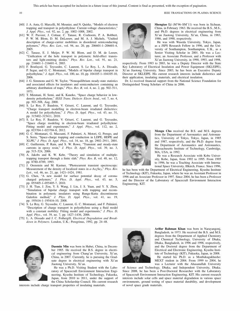
Daomin Min was born in Hubei, China, in Decem-ber 1985. He received the B.S. degree in electri-cal engineering from Chang’an University, Xi’an,China, in 2007. Currently, he is pursuing the Grad-uate degree in electrical engineering with Xi’anJiaotong University, Xi’an.
He was a Ph.D. Visiting Student with the Labo-ratory of Spacecraft Environment Interaction Engi-neering, Kyushu Institute of Technology, Fukuoka,Japan, from 2010 to 2011, under the support ofthe China Scholarship Council. His current research
interests include charge transport properties of insulating materials.
Shengtao Li (M’96–SM’11) was born in Sichuan,China, in February 1963. He received the B.S., M.S.,and Ph.D. degrees in electrical engineering fromXi’an Jiaotong University, Xi’an, China, in 1983,1986, and 1990, respectively.
He was with Waseda University, Tokyo, Japan,as a JSPS Research Fellow in 1996, and the Uni-versity of Southampton, Southampton, U.K., as aSenior Visiting Scholar in 2001. He was a Lec-turer, an Associate Professor, and a Professor withXi’an Jiaotong University, in 1990, 1993, and 1998,
respectively. From 1993 to 2003, he was a Deputy Director with the StateKey Laboratory of Electrical Insulation and Power Equipment (SKLEIPE),Xi’an Jiaotong University. Since 2003, he has been an Executive DeputyDirector at SKLEIPE. His current research interests include dielectrics andtheir application, insulating materials, and electrical insulation.
Dr. Li received financial support from the National Science Foundation forDistinguished Young Scholars of China in 2006.
Mengu Cho received the B.S. and M.S. degreesfrom the Department of Aeronautics and Astronau-tics, University of Tokyo, Tokyo, Japan, in 1985and 1987, respectively, and the Ph.D. degree fromthe Department of Aeronautics and Astronautics,Massachusetts Institute of Technology, Cambridge,MA, USA, in 1992.
He was a Research Associate with Kobe Univer-sity, Kobe, Japan, from 1992 to 1995. From 1995to 1996, he was a Teaching Associate with Interna-tional Space University, Illkirch, France. Since 1996,
he has been with the Department of Electrical Engineering, Kyushu Instituteof Technology (KIT), Fukuoka, Japan, where he was an Assistant Professor in1996 and an Associate Professor in 1997. Since 2004, he has been a Professorand the Director of the Laboratory of Spacecraft Environment InteractionEngineering, KIT.
Arifur Rahman Khan was born in Narayangonj,Bangladesh, in 1973. He received the B.S. and M.S.degrees from the Department of Applied Chemistryand Chemical Technology, University of Dhaka,Dhaka, Bangladesh, in 1996 and 1998, respectively,and the Doctoral degree from the Department ofElectrical and Electronic Engineering, Kyushu Insti-tute of Technology (KIT), Fukuoka, Japan, in 2008.
He started his Ph.D. as a Monbukagakhusho:MEXT student in 2004. From 1999 to 2004, hewas a Lecturer with the Ahasanullah University
of Science and Technology, Dhaka, and Independent University, Dhaka.Since 2008, he has been a Post-Doctoral Researcher with the Laboratoryof Spacecraft Environment Interaction Engineering, KIT. His current researchinterests include solar cells and space material degradation in various spaceenvironments, ground testing of space material durability, and developmentof novel space grade materials.