Embed Size (px)
Citation preview
ADLEEPOWER
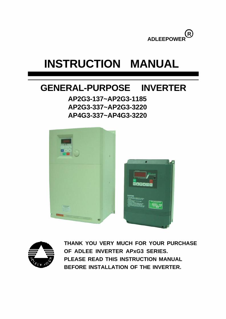
INSTRUCTION MANUAL
GENERAL-PURPOSE INVERTER
THANK YOU VERY MUCH FOR YOUR PURCHASEOF ADLEE INVERTER APxG3 SERIES.PLEASE READ THIS INSTRUCTION MANUALBEFORE INSTALLATION OF THE INVERTER.
R
AP2G3-137~AP2G3-1185AP2G3-337~AP2G3-3220AP4G3-337~AP4G3-3220
CONTENTS
1. RECEIVING
2. SPECIFICATIONS
3. DIMENSION DRAWINGS
4. INSTALLATION
5. DESCRIPTION OF TERMINALS
6. DIGITAL OPERATION PANEL
7. FUNCTIONS DESCRIPTION
8. PROTECTIVE FUNCTIION
9. PRECAUTIONS
10. TROUBLESHOOTING
11. APPLICATION
12. INVERTER SELECTION
13. APPENDIX
A. Optional braking resistor
B. Terminal wiring diagram
C. Remote operator
1
2
4
6
8
18
19
73
77
78
79
85
89
89
90
91
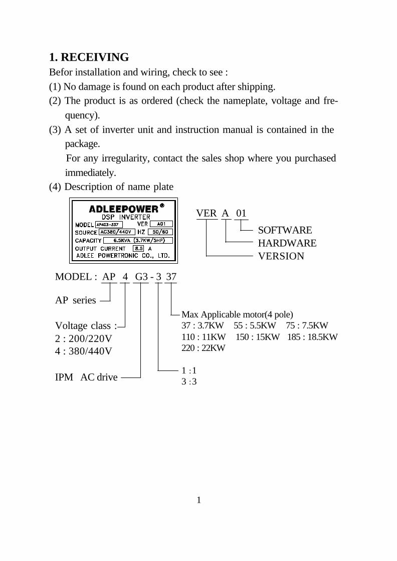
1. RECEIVINGBefor installation and wiring, check to see :(1) No damage is found on each product after shipping.(2) The product is as ordered (check the nameplate, voltage and fre- quency).(3) A set of inverter unit and instruction manual is contained in the package. For any irregularity, contact the sales shop where you purchased immediately.(4) Description of name plate
VER A 01
SOFTWAREHARDWAREVERSION
MODEL : AP 4 G3 - 3 37
Max Applicable motor(4 pole)37 : 3.7KW 55 : 5.5KW 75 : 7.5KW110 : 11KW 150 : 15KW 185 : 18.5KW220 : 22KW
1 : 13 : 3
AP series
Voltage class :2 : 200/220V4 : 380/440V
IPM AC drive
1
∮ ∮
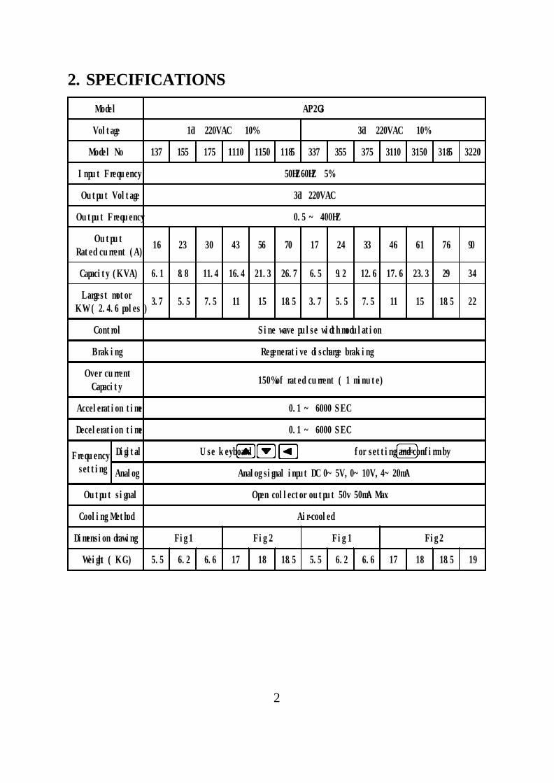
2. SPECIFICATIONS
2
PROG
Model AP2G3
Voltage 1φ 220VAC ± 10% 3φ 220VAC ± 10%
Model No137 155 175111011501185337 355 3753110315031853220
Input Frequency 50HZ/60HZ ±5%
Output Voltage 3φ 220VAC
Output Frequency 0.5 ~ 400HZ
OutputRated current (A)
16 23 30 43 56 70 17 24 33 46 61 76 90
Capacity (KVA)6.18.811.416.421.326.76.59.212.617.623.329 34
Largest motorKW ( 2.4.6 poles )
3.7 5.57.5 11 15 18.53.75.57.5 11 15 18.522
Control Sine wave pulse width modulation
Braking Regenerative discharge braking
Over currentCapacity 150% of rated current ( 1 minute)
Acceleration time 0.1 ~ 6000 SEC
Deceleration time 0.1 ~ 6000 SEC
Frequencysetting
Digital Use keyboard for setting and confirm by
Analog Analog signal input DC 0~5V, 0~10V, 4~20mA
Output signal Open collector output 50v 50mA Max
Cooling Method Air-cooled
Dimension drawingFig 1 Fig 2 Fig 1 Fig 2
Weight ( KG )5.56.26.6 17 18 18.55.56.26.6 17 18 18.519
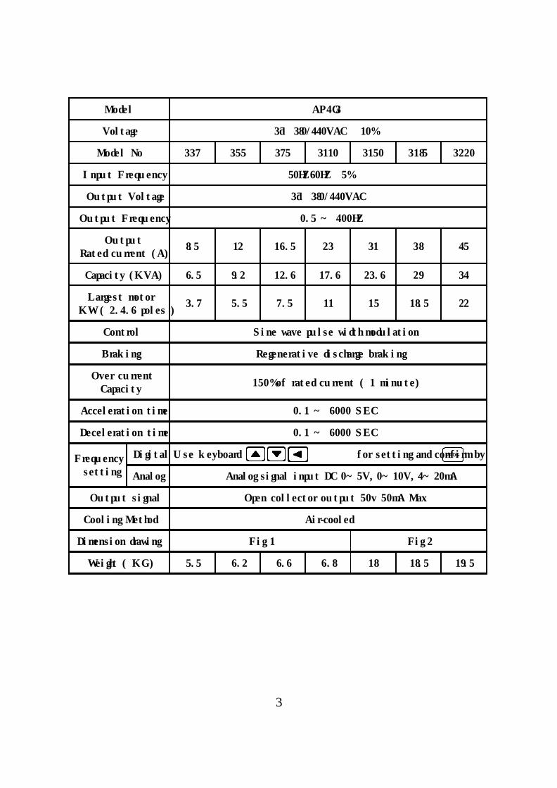
PROG
3
Model AP4G3
Voltage 3φ 380/440VAC ±10%
Model No337 355 375 3110315031853220
Input Frequency 50HZ/60HZ ±5%
Output Voltage 3φ 380/440VAC
Output Frequency 0.5 ~ 400HZ
OutputRated current (A)
8.5 12 16.5 23 31 38 45
Capacity (KVA)6.5 9.2 12.617.623.6 29 34
Largest motorKW ( 2.4.6 poles )
3.7 5.5 7.5 11 15 18.5 22
Control Sine wave pulse width modulation
Braking Regenerative discharge braking
Over currentCapacity 150% of rated current ( 1 minute)
Acceleration time 0.1 ~ 6000 SEC
Deceleration time 0.1 ~ 6000 SEC
Frequencysetting
DigitalUse keyboard for setting and confirm by
Analog Analog signal input DC 0~5V, 0~10V, 4~20mA
Output signal Open collector output 50v 50mA Max
Cooling Method Air-cooled
Dimension drawingFig 1 Fig 2
Weight ( KG )5.5 6.2 6.6 6.8 18 18.519.5
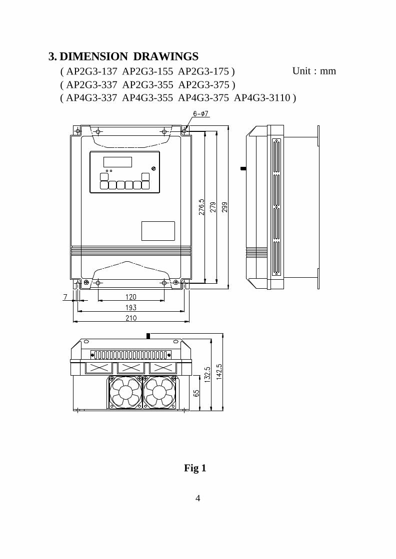
3. DIMENSION DRAWINGS ( AP2G3-137 AP2G3-155 AP2G3-175 ) ( AP2G3-337 AP2G3-355 AP2G3-375 ) ( AP4G3-337 AP4G3-355 AP4G3-375 AP4G3-3110 )
Fig 1
Unit : mm
4
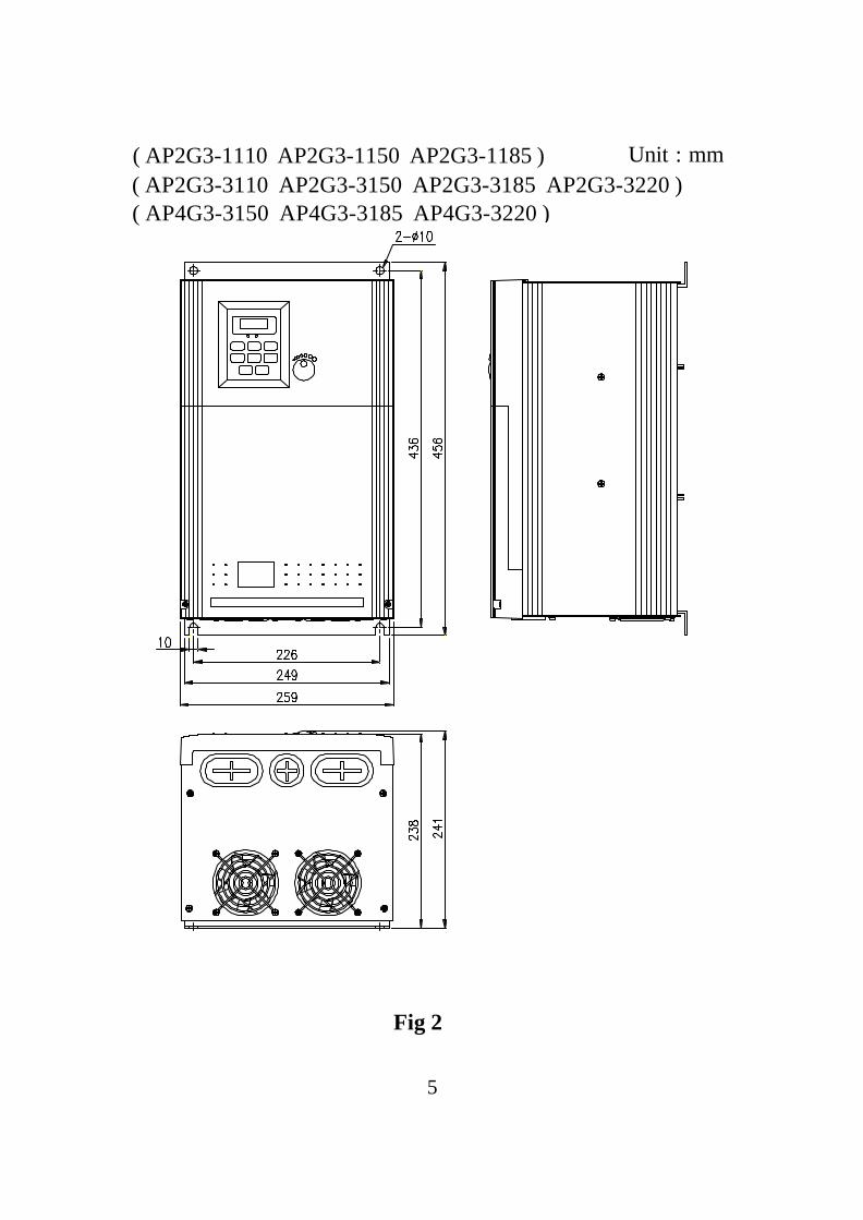
Fig 2
Unit : mm
5
( AP2G3-1110 AP2G3-1150 AP2G3-1185 ) ( AP2G3-3110 AP2G3-3150 AP2G3-3185 AP2G3-3220 ) ( AP4G3-3150 AP4G3-3185 AP4G3-3220 )
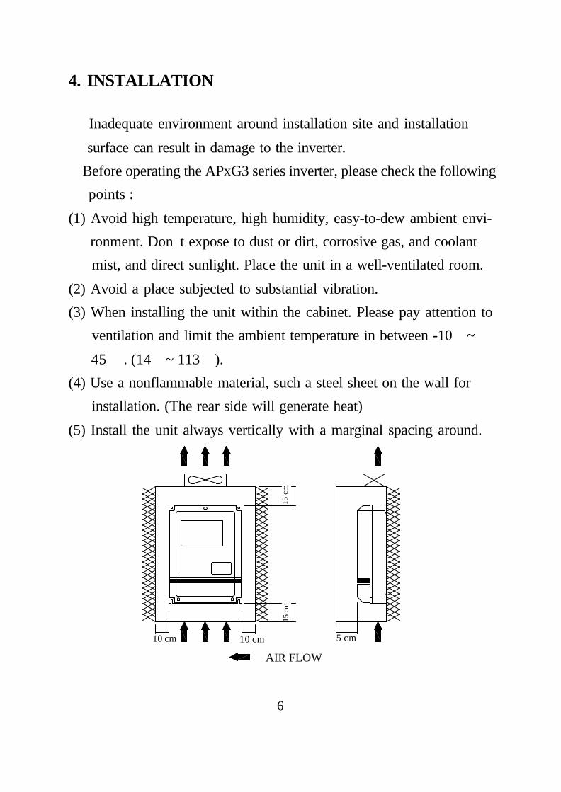
4. INSTALLATION
Inadequate environment around installation site and installation
surface can result in damage to the inverter.
Before operating the APxG3 series inverter, please check the following
points :
(1) Avoid high temperature, high humidity, easy-to-dew ambient envi-
ronment. Don’t expose to dust or dirt, corrosive gas, and coolant
mist, and direct sunlight. Place the unit in a well-ventilated room.
(2) Avoid a place subjected to substantial vibration.
(3) When installing the unit within the cabinet. Please pay attention to
ventilation and limit the ambient temperature in between -10℃ ~
45℃ . (14℉ ~ 113℉ ).
(4) Use a nonflammable material, such a steel sheet on the wall for
installation. (The rear side will generate heat)
(5) Install the unit always vertically with a marginal spacing around.
6
AIR FLOW
15 c
m15
cm
5 cm10 cm10 cm
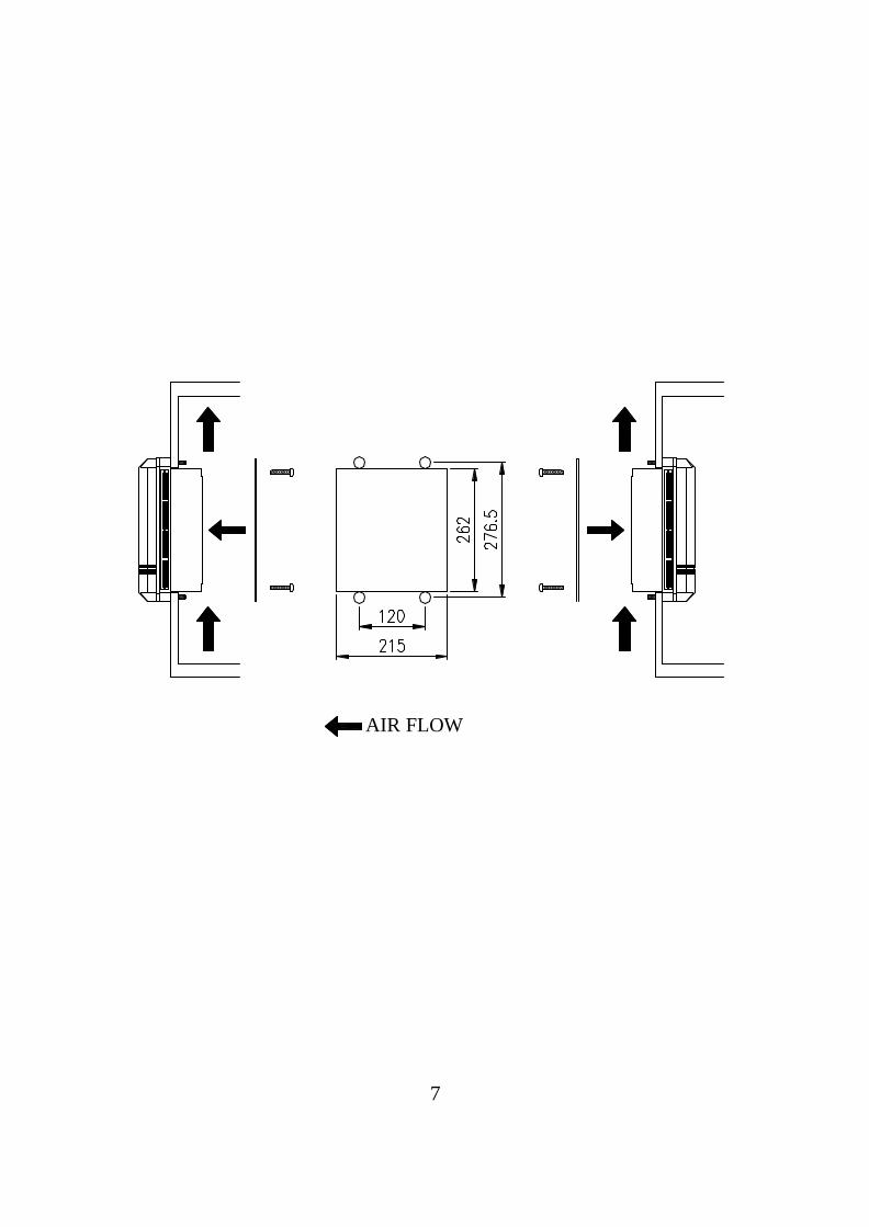
7
AIR FLOW
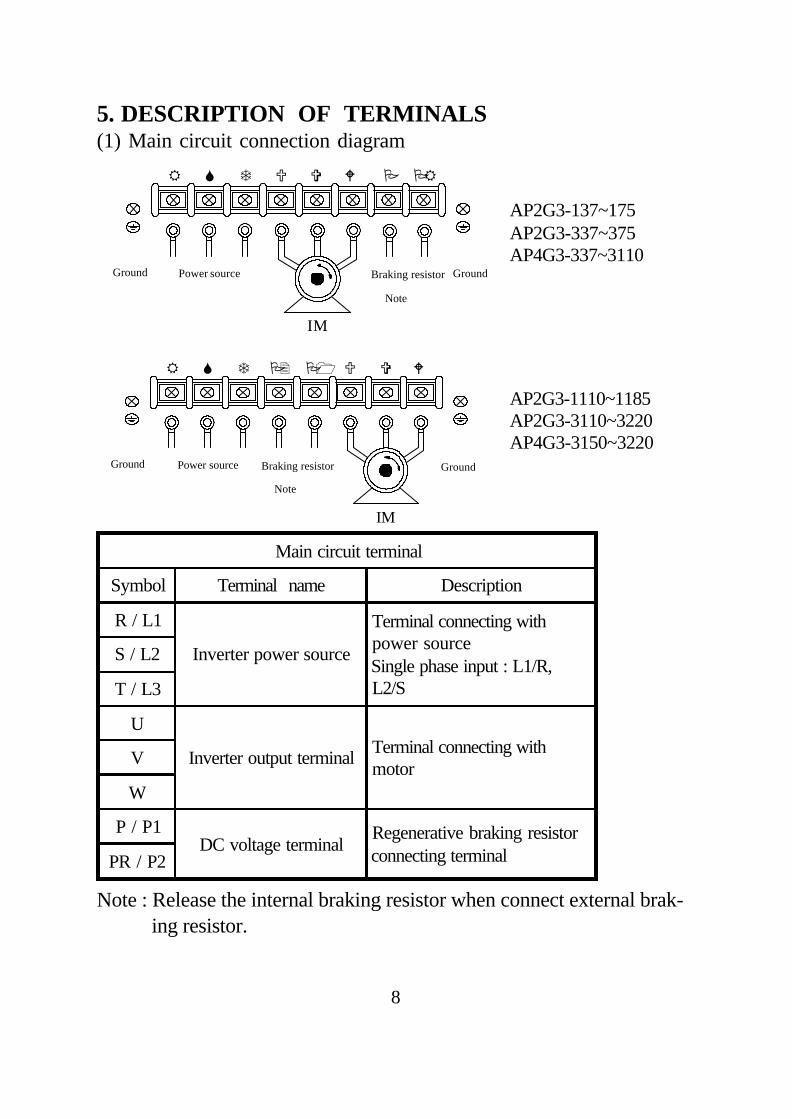
5. DESCRIPTION OF TERMINALS(1) Main circuit connection diagram
8
R S T P2 P1 U V W
IM
Ground Power source Braking resistor
(★Note)
Ground
AP2G3-137~175AP2G3-337~375AP4G3-337~3110
AP2G3-1110~1185AP2G3-3110~3220AP4G3-3150~3220
Note : Release the internal braking resistor when connect external brak- ing resistor.
Main circuit terminal
Symbol Terminal name Description
R / L1
Inverter power source
Terminal connecting withpower sourceSingle phase input : L1/R,L2/S
S / L2
T / L3
U
Inverter output terminal Terminal connecting withmotorV
W
P / P1DC voltage terminal
Regenerative braking resistorconnecting terminalPR / P2
R S T U V W P PR
IM
Ground Power source Braking resistor
(★Note)
Ground
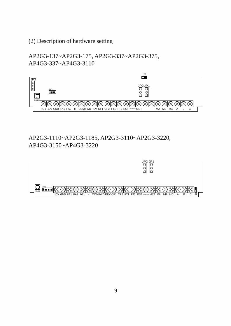
(2) Description of hardware setting
AP2G3-137~AP2G3-175, AP2G3-337~AP2G3-375,AP4G3-337~AP4G3-3110
AP2G3-1110~AP2G3-1185, AP2G3-3110~AP2G3-3220,AP4G3-3150~AP4G3-3220
GND FA1 FA2 H COMFWD REV CF1 CF2 FT1 FT2 RST ARR/RUN MET -
JP3
MB+ MA AMC B C
RS485
SW1
1 32 4
10VFG1
JP1
J3
JP2
10V GND FA1 FA2 FG1 H COMFWD REV CF1 CF2 FT1 FT2 RST ARR/RUN
SW1
1 2 3 4
JP1
MBMET MA AMC B C J4RS485 5 6
JP2
9
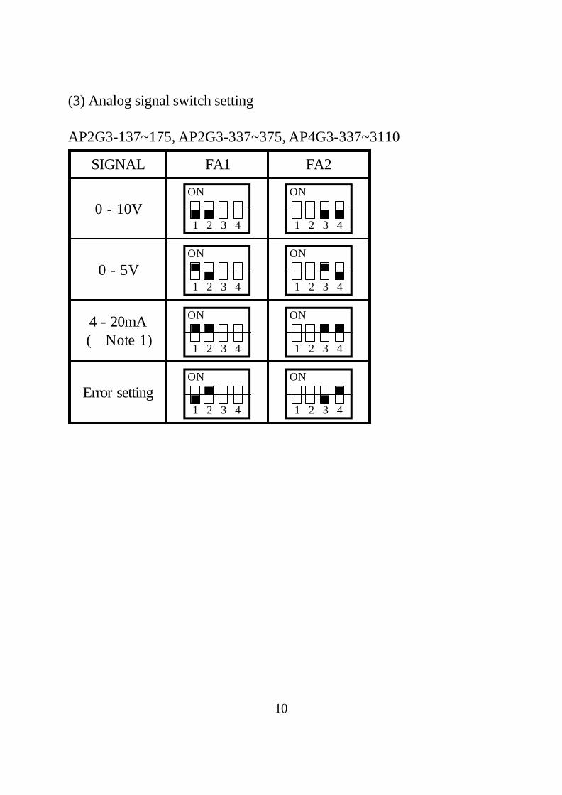
(3) Analog signal switch setting
AP2G3-137~175, AP2G3-337~375, AP4G3-337~3110
ON
1 2 3 4
ON
1 2 3 4
SIGNAL FA1 FA2
0 - 10V
0 - 5V
4 - 20mA( Note 1)★
Error setting
ON
1 2 3 4
ON
1 2 3 4
ON
1 2 3 4
ON
1 2 3 4
ON
1 2 3 4
ON
1 2 3 4
10
11
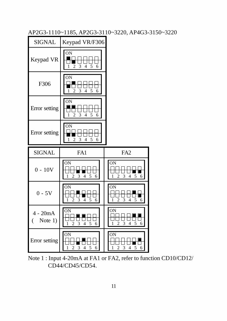
AP2G3-1110~1185, AP2G3-3110~3220, AP4G3-3150~3220
SIGNAL Keypad VR/F306
Keypad VR
F306
Error setting
Error setting
ON
1 2 3 4 5 6
ON
1 2 3 4 5 6
ON
1 2 3 4 5 6
ON
1 2 3 4 5 6
Note 1 : Input 4-20mA at FA1 or FA2, refer to function CD10/CD12/ CD44/CD45/CD54.
SIGNAL FA1 FA2
0 - 10V
0 - 5V
4 - 20mA( Note 1)★
Error setting
ON
1 2 3 4 5 6
ON
1 2 3 4 5 6
ON
1 2 3 4 5 6
ON
1 2 3 4 5 6
ON
1 2 3 4 5 6
ON
1 2 3 4 5 6
ON
1 2 3 4 5 6
ON
1 2 3 4 5 6
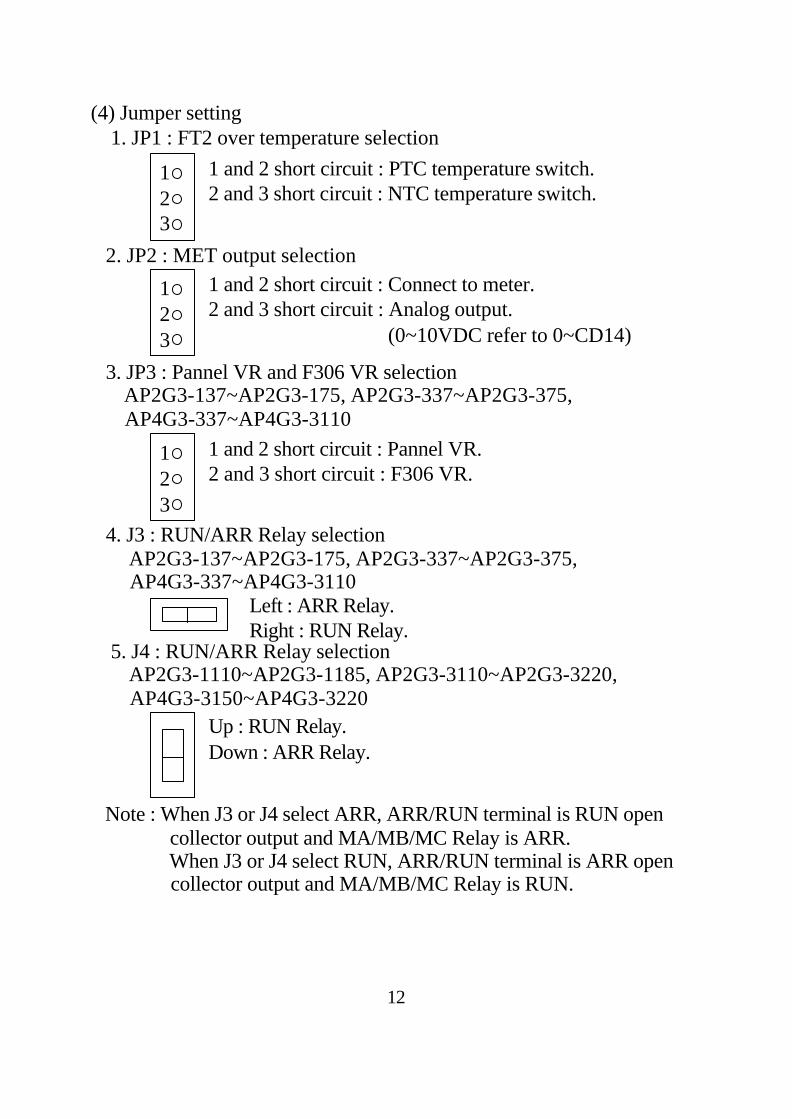
(4) Jumper setting 1. JP1 : FT2 over temperature selection
2. JP2 : MET output selection
3. JP3 : Pannel VR and F306 VR selection AP2G3-137~AP2G3-175, AP2G3-337~AP2G3-375, AP4G3-337~AP4G3-3110
4. J3 : RUN/ARR Relay selection AP2G3-137~AP2G3-175, AP2G3-337~AP2G3-375, AP4G3-337~AP4G3-3110
5. J4 : RUN/ARR Relay selection AP2G3-1110~AP2G3-1185, AP2G3-3110~AP2G3-3220, AP4G3-3150~AP4G3-3220
Note : When J3 or J4 select ARR, ARR/RUN terminal is RUN open collector output and MA/MB/MC Relay is ARR. When J3 or J4 select RUN, ARR/RUN terminal is ARR open collector output and MA/MB/MC Relay is RUN.
12
1 and 2 short circuit : PTC temperature switch.2 and 3 short circuit : NTC temperature switch.
123
1 and 2 short circuit : Pannel VR.2 and 3 short circuit : F306 VR.
123
Left : ARR Relay.Right : RUN Relay.
Up : RUN Relay.Down : ARR Relay.
1 and 2 short circuit : Connect to meter.2 and 3 short circuit : Analog output. (0~10VDC refer to 0~CD14)
123
13
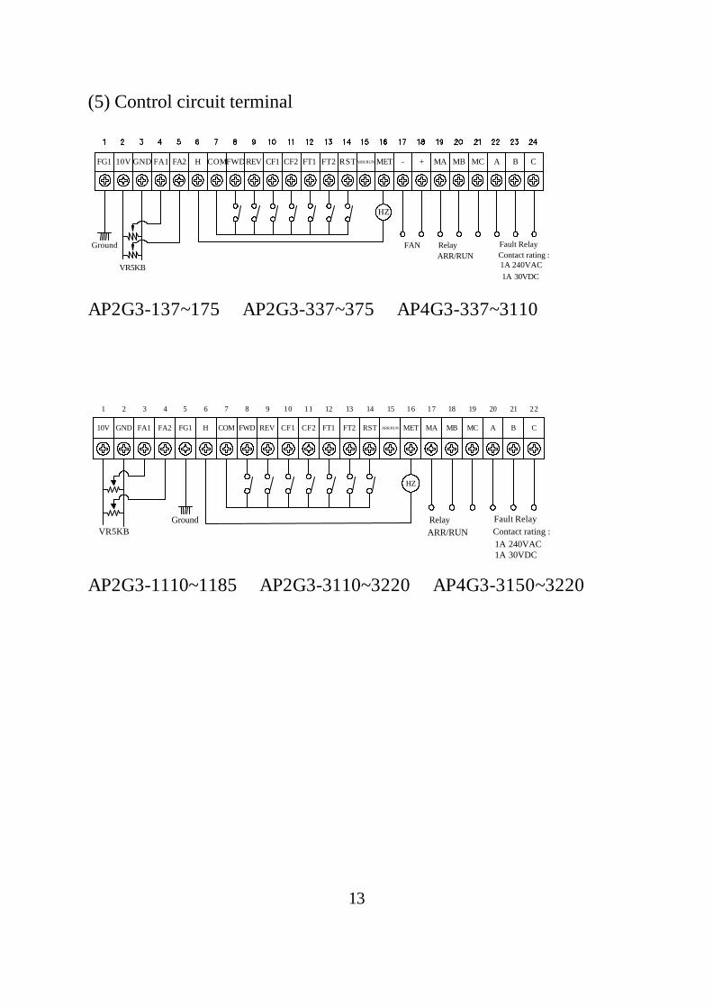
(5) Control circuit terminal
AP2G3-137~175、AP2G3-337~375、AP4G3-337~3110
AP2G3-1110~1185、AP2G3-3110~3220、AP4G3-3150~3220
10V GND FA1 FA2 FG1 H COM REV CF1 CF2 FT1 FT2 RST ARR/RUN MET MA MB MC A
16321 10654 987 131211 1514 191817 20
B
21
C
22
FWD
HZ
Contact rating :ARR/RUN1A 240VAC
Relay Fault RelayVR5KB
Ground
1A 30VDC
FG1 10V GND FA1 FA2 H COMFWD REV CF1 CF2 FT1 FT2 RSTARR/RUN MET - + MA MB
VR5KB
Fault RelayContact rating :
1A 30VDC
HZ
BAMC C
ARR/RUNRelay FANGround
1A 240VAC
CF1 CF2 SPEED
OFF OFF SPEED - 1
ON OFF SPEED - 2
OFF ON SPEED - 3
ON ON SPEED - 4
14
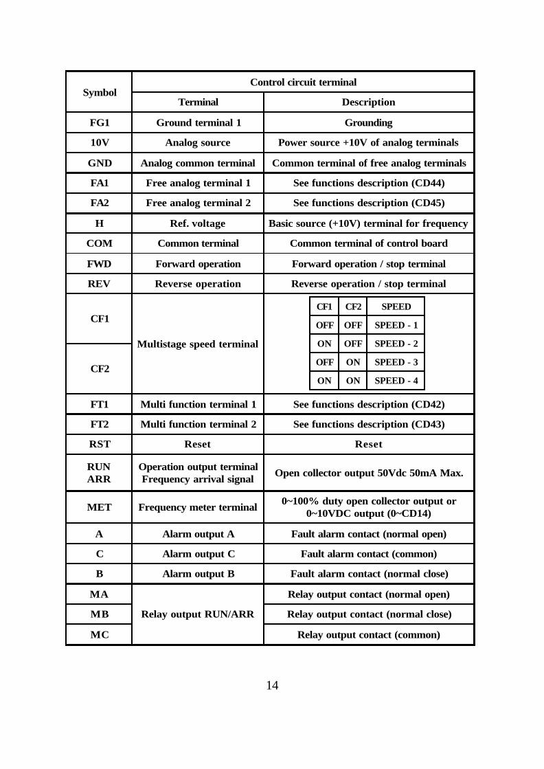
SymbolControl circuit terminal
Terminal Description
FG1 Ground terminal 1 Grounding
10V Analog source Power source +10V of analog terminals
GND Analog common terminal Common terminal of free analog terminals
FA1 Free analog terminal 1 See functions description (CD44)
FA2 Free analog terminal 2 See functions description (CD45)
H Ref. voltage Basic source (+10V) terminal for frequency
COM Common terminal Common terminal of control board
FWD Forward operation Forward operation / stop terminal
REV Reverse operation Reverse operation / stop terminal
CF1
Multistage speed terminal
CF2
FT1 Multi function terminal 1 See functions description (CD42)
FT2 Multi function terminal 2 See functions description (CD43)
RST Reset Reset
RUNARR
Operation output terminalFrequency arrival signal Open collector output 50Vdc 50mA Max.
MET Frequency meter terminal 0~100% duty open collector output or0~10VDC output (0~CD14)
A Alarm output A Fault alarm contact (normal open)
C Alarm output C Fault alarm contact (common)
B Alarm output B Fault alarm contact (normal close)
MA
Relay output RUN/ARR
Relay output contact (normal open)
MB Relay output contact (normal close)
MC Relay output contact (common)
L1/R
L2/S
U
V
W
APxG3-Series
IM
THRY
E
POWER SOURCE
L3/T
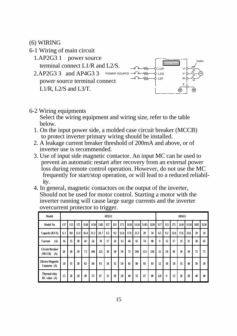
(6) WIRING6-1 Wiring of main circuit 1.AP2G3 1 power source terminal connect L1/R and L2/S. 2.AP2G3 3 and AP4G3 3 power source terminal connect L1/R, L2/S and L3/T.
6-2 Wiring equipments Select the wiring equipment and wiring size, refer to the table below. 1. On the input power side, a molded case circuit breaker (MCCB) to protect inverter primary wiring should be installed. 2. A leakage current breaker threshold of 200mA and above, or of inverter use is recommended. 3. Use of input side magnetic contactor. An input MC can be used to prevent an automatic restart after recovery from an external power loss during remote control operation. However, do not use the MC frequently for start/stop operation, or will lead to a reduced reliabil- ity. 4. In general, magnetic contactors on the output of the inverter, Should not be used for motor control. Starting a motor with the inverter running will cause large surge currents and the inverter overcurrent protector to trigger.
15
Model AP2G3 AP4G3
Model No 137 155 175 1110 1150 1185 337 355 375 3110 3150 3185 3220 337 355 375 3110 3150 3185 3220
Capacity (KVA) 6.1 8.8 11.4 16.4 21.3 26.7 6.5 9.2 12.6 17.6 23.3 29 34 6.5 9.2 12.6 17.6 23.6 29 34
Current (A) 16 23 30 43 56 70 17 24 33 46 61 76 90 9 12 17 23 31 38 45
Circuit Breaker(MCCB) (A) 20 30 50 75 100 125 20 30 50 75 100 125 150 15 20 30 50 50 75 75
Electro-MagneticContactor (A) 18 35 50 65 80 93 18 35 50 65 80 93 93 12 18 18 35 48 50 50
Thermal relayRC value (A) 15 20 28 40 55 67 15 20 28 40 55 67 80 6.8 9 15 20 28 40 40
∮
∮ ∮
6-3 Surge absorber
In order to prevent malfunction, provide the surge absorber on the coils of the electromagnetic contactors, relays and other devices which are to be used adjacent of the inverter.
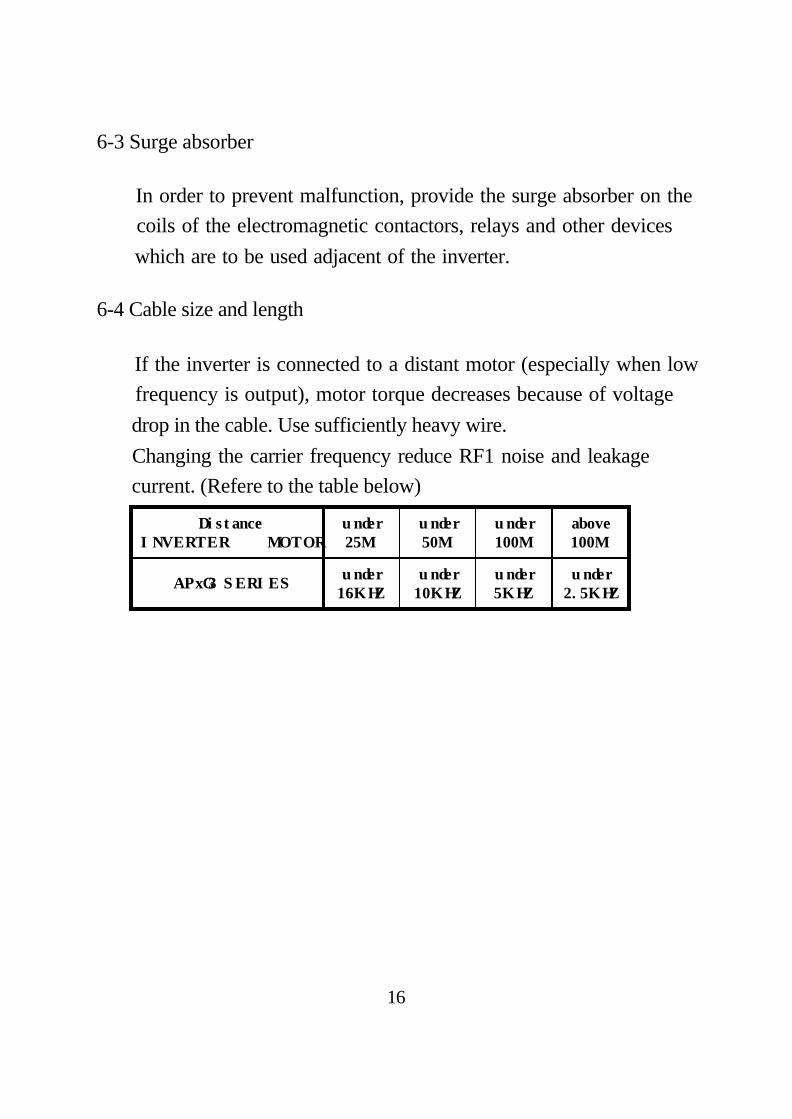
6-4 Cable size and length
If the inverter is connected to a distant motor (especially when low frequency is output), motor torque decreases because of voltage drop in the cable. Use sufficiently heavy wire. Changing the carrier frequency reduce RF1 noise and leakage current. (Refere to the table below)
16
DistanceINVERTER → MOTOR
under25M
under50M
under100M
above100M
APxG3 SERIESunder16KHZ
under10KHZ
under5KHZ
under2.5KHZ
(a) (b) (c)
17
6-5 Wiring and cautionary points A. Main circuit 1. Don’t connect the cables of the power supply side (L1/R,L2/S,L3/ T) to the U, V and W output terminals for the motor. 2. Don’t connect any electromagnetic contactor between the inverter and motor. If it is inevitable, turn on the contactor when both the inverter and motor are both at stand still. 3. Don’t put the advance phase capacitor between the inverter and motor. 4. Put MCCB in the input power supply.
B. Control signal circuit 1. Separate the power cables of main circuit etc. from the control cables of the sequence and analog signals by passing the cables through the different ducts. 2. Use twisted pair shielded wire for control signal and connect the shield to earth terminal at on end, COMMON terminal of control board. Leave the other end of shielding open. 3. Avoid common Ground leads between high and low level voltage equipment.
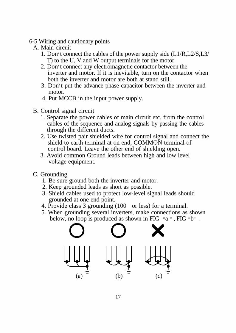
C. Grounding 1. Be sure ground both the inverter and motor. 2. Keep grounded leads as short as possible. 3. Shield cables used to protect low-level signal leads should grounded at one end point. 4. Provide class 3 grounding (100Ω or less) for a terminal. 5. When grounding several inverters, make connections as shown below, no loop is produced as shown in FIG “a “ , FIG “b“ .
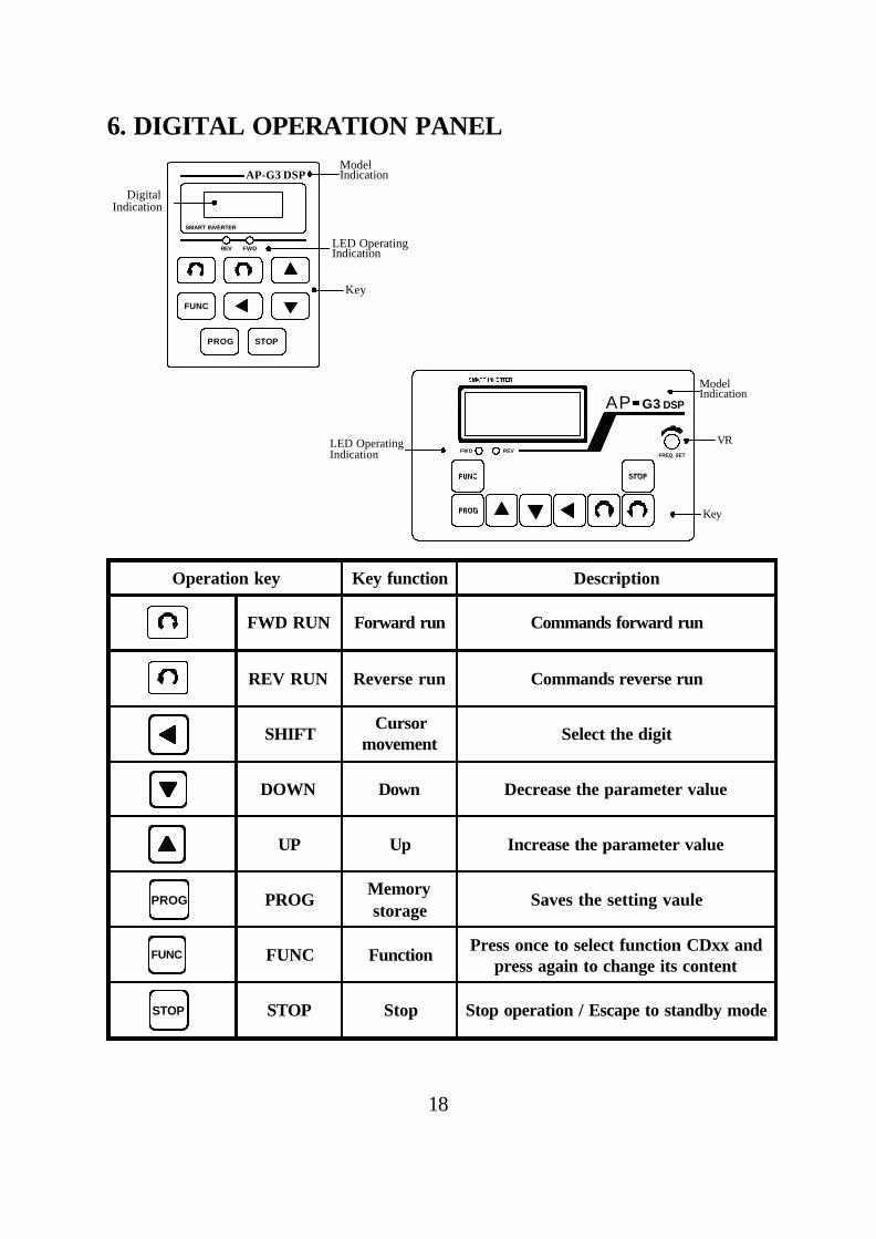
6. DIGITAL OPERATION PANEL
Operation key Key function Description
FWD RUN Forward run Commands forward run
REV RUN Reverse run Commands reverse run
SHIFTCursor
movement Select the digit
DOWN Down Decrease the parameter value
UP Up Increase the parameter value
PROGMemorystorage
Saves the setting vaule
FUNC Function Press once to select function CDxx andpress again to change its content
STOP Stop Stop operation / Escape to standby mode
18
PROG
FUNC
STOP
FWDFREQ. SET
REV
AP G3 DSP
ModelIndication
VR
Key
LED OperatingIndication
AP-G3 DSP
SMART INVERTER
PROG STOP
FUNC
FWDREV
IndicationModel
Key
DigitalIndication
IndicationLED Operating
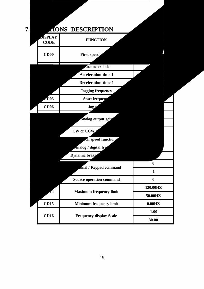
7. FUNCTIONS DESCRIPTION
19
DISPLAYCODE
FUNCTION DEFAULT VALUE
☆ CD00 First speed setting60.00HZ
50.00HZ
CD01 Parameter lock 0
CD02 Acceleration time 1 10.0Sec
CD03 Deceleration time 1 10.0Sec
CD04 Jogging frequency 5.00HZ
CD05 Start frequency 0.50HZ
CD06 Jog mode 0
☆ CD07 Analog output gain120.00HZ
100.00HZ
CD08 CW or CCW or CW / CCW 0
CD09 Search speed function 0
CD10 Analog / digital frequency 1
CD11 Dynamic brake / Free running 0
☆ CD12 Terminal / Keypad command0
1
CD13 Source operation command 0
☆ CD14 Maximum frequency limit120.00HZ
50.00HZ
CD15 Minimum frequency limit 0.00HZ
☆ CD16 Frequency display Scale1.00
30.00
20
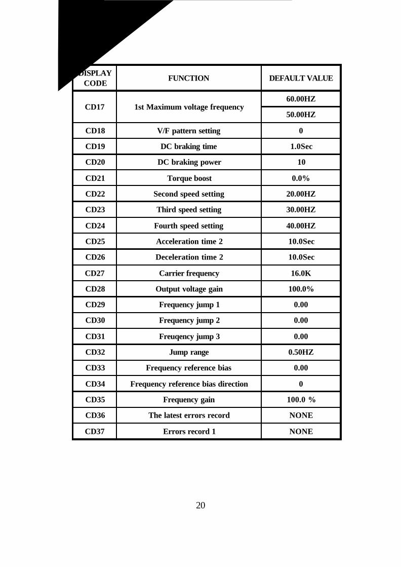
DISPLAYCODE
FUNCTION DEFAULT VALUE
☆ CD17 1st Maximum voltage frequency60.00HZ
50.00HZ
CD18 V/F pattern setting 0
CD19 DC braking time 1.0Sec
CD20 DC braking power 10
CD21 Torque boost 0.0%
CD22 Second speed setting 20.00HZ
CD23 Third speed setting 30.00HZ
CD24 Fourth speed setting 40.00HZ
CD25 Acceleration time 2 10.0Sec
CD26 Deceleration time 2 10.0Sec
CD27 Carrier frequency 16.0K
CD28 Output voltage gain 100.0%
CD29 Frequency jump 1 0.00
CD30 Frequency jump 2 0.00
CD31 Freuqency jump 3 0.00
CD32 Jump range 0.50HZ
CD33 Frequency reference bias 0.00
CD34 Frequency reference bias direction 0
CD35 Frequency gain 100.0 %
CD36 The latest errors record NONE
CD37 Errors record 1 NONE
21
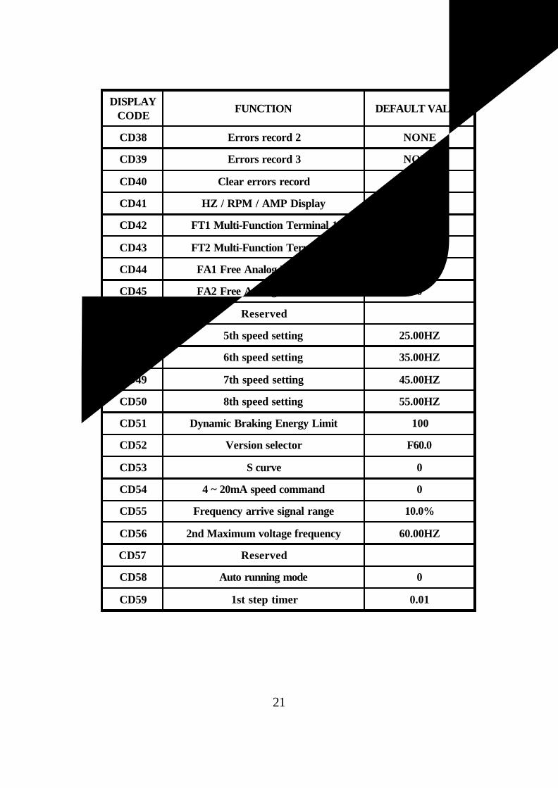
DISPLAYCODE
FUNCTION DEFAULT VALUE
CD38 Errors record 2 NONE
CD39 Errors record 3 NONE
CD40 Clear errors record 0
CD41 HZ / RPM / AMP Display 0
CD42 FT1 Multi-Function Terminal 1 0
CD43 FT2 Multi-Function Terminal 2 0
CD44 FA1 Free Analog Terminal 1 0
CD45 FA2 Free Analog Terminal 2 0
CD46 Reserved
CD47 5th speed setting 25.00HZ
CD48 6th speed setting 35.00HZ
CD49 7th speed setting 45.00HZ
CD50 8th speed setting 55.00HZ
CD51 Dynamic Braking Energy Limit 100
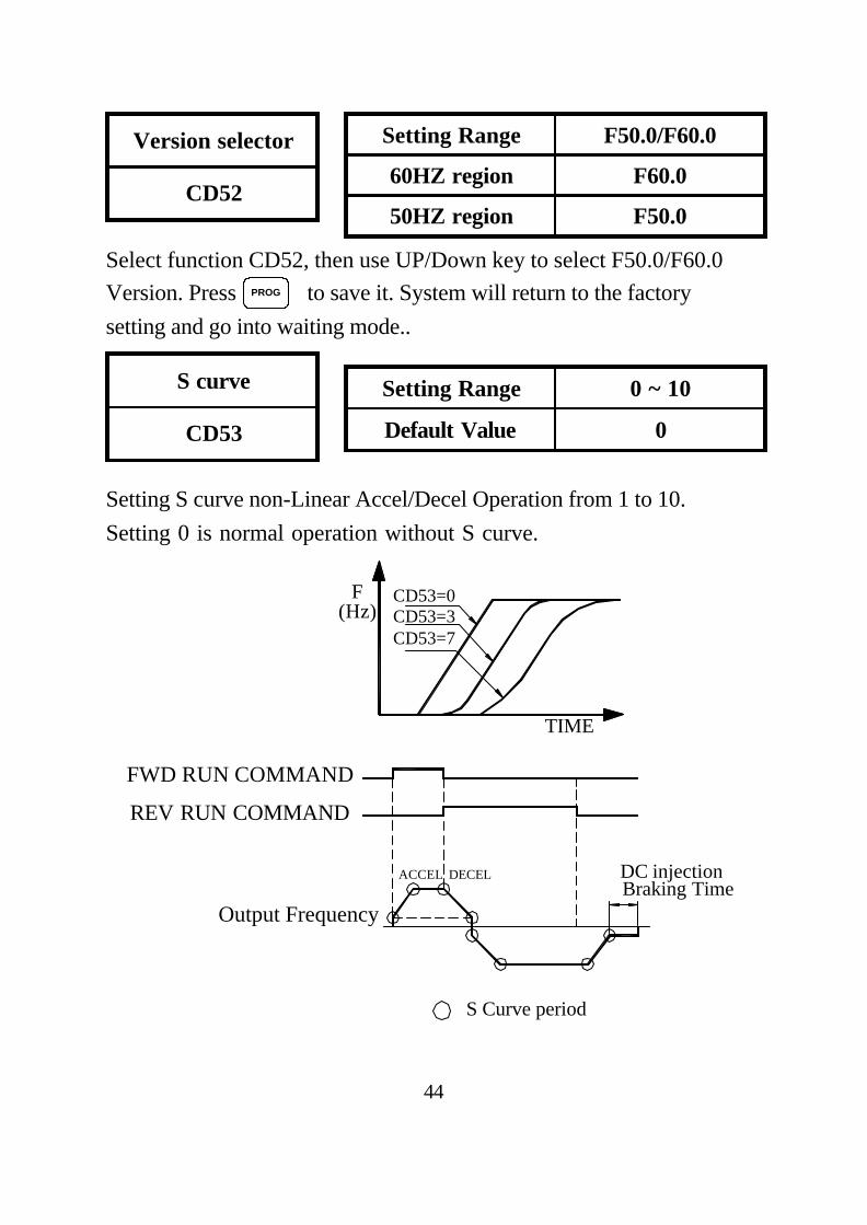
☆ CD52 Version selector F60.0
CD53 S curve 0
CD54 4 ~ 20mA speed command 0
CD55 Frequency arrive signal range 10.0%
CD56 2nd Maximum voltage frequency 60.00HZ
CD57 Reserved
CD58 Auto running mode 0
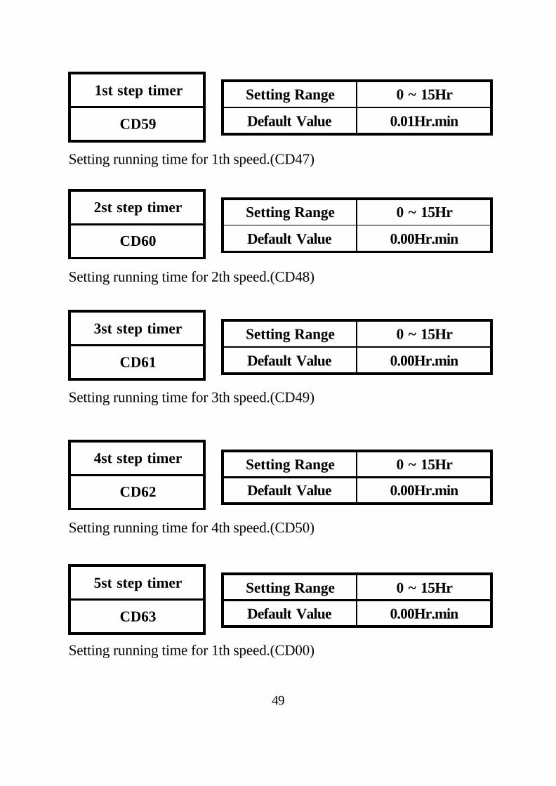
CD59 1st step timer 0.01
22
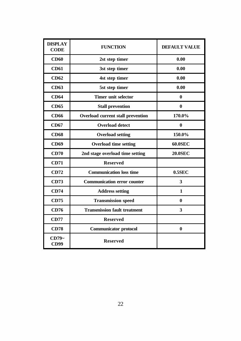
DISPLAYCODE FUNCTION DEFAULT VALUE
CD60 2st step timer 0.00
CD61 3st step timer 0.00
CD62 4st step timer 0.00
CD63 5st step timer 0.00
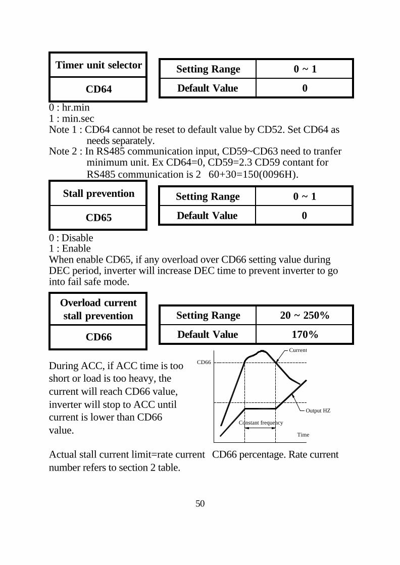
CD64 Timer unit selector 0
CD65 Stall prevention 0
CD66 Overload current stall prevention 170.0%
CD67 Overload detect 0
CD68 Overload setting 150.0%
CD69 Overload time setting 60.0SEC
CD70 2nd stage overload time setting 20.0SEC
CD71 Reserved
CD72 Communication loss time 0.5SEC
CD73 Communication error counter 3
CD74 Address setting 1
CD75 Transmission speed 0
CD76 Transmission fault treatment 3
CD77 Reserved
CD78 Communicator protocol 0
CD79~CD99
Reserved
☆ Different initial set value for F50.0 : 50HZ power region and F60.0 : 60HZ power region. To change version see description of CD52. This function provides different standard setting values for 50/60HZ power region. F60.0 : 60HZ region for USA, CANADA etc. F50.0 : 50HZ region for Europe, Australia, Singapore etc.☆ CD13 after finished parameter setting, please repower “ON”.
23
Communication address description
DISPLAYCODE FUNCTION UNIT
100 Speed command for RS485 3
101 Frequency data output for RS485 0.01HZ
102 Current data output for RS485 0.1A
103 Fault code for RS485
7-1. Function setting
Before starting test run, check carefully the following points :
(1) Be sure to connect the power supply to L1/R, L2/S, L3/T (input
terminals) and the motor to U.V.W. (output terminals). (Wrong
connections will damage the inverter.)
(2) Check that the input power supply is 220VAC± 10%, 50/60HZ± 5%
for AP2G3 and 380~440VAC± 10%, 50/60HZ± 5% for AP4G3 series.
(3) Check the signal lines for wrong wiring.
(4) Be sure to ground an earth terminal for personnel safety.
(5) Check that other terminals than earth terminal are not grounded.
(6) Check that the inverter is mounted on the wall. Also check that
non-flammable material, U. V. W.(output terminals). (Wrong connec-
tion will damage the inverter.)
(7) For operation start and stop, use and FWD / REV
terminals. Never use input power supply to switch ON/OFF.
24
STOP
Operation
1-1. Pannel
Action : (a) Press for forward / reverse operation.
Speed : (a) Using to change motor speed with 1HZ
increment step. or to select the digit for quick
setting and confirm by .
Standby : (a) Press back to standby mode after trip or function
setting mode.
1-2. F306
Set CD13=1 and repower “ON”, operation same as 1-1 pannel.
1-3. RS485 communication control
Set CD13=2 and set CD74~CD78. (Refer to CD74~CD78).
Using 06H function write command to address 100(64H).
1 : CW, 2 : CCW, 3 : Stop, 4 : Clear fault.
1-4. Terminal control
Set CD12=1, writing refer to 5-5 control circuit terminal wiring
digaram.
PROG
STOP
25
Press key for increase or decrease the speed with 1HZ
increment .
Press key to select the digit for quick setting.
Press to save the setting value.
0 : Lock 1 : Unlock
Function to prevent inadequate setting.
To change the contents data of CD , set CD01=1 and press first.
To lock the data set CD01=0 and press .
CD02 value corresponds to thetime of acceleration from 0 to 50/60HZ.(For 120Hz. setting, thearrival time to 120Hz is double.)
F60HZ
0.1 6000 TIME(Sec)
First speed setting
CD00
Parameter lock
CD01
Acceleration time 1
CD02
26
PROG
PROG
PROG
Setting Range 0 or 1
Default Value 0
Setting Range 0.1 ~ 6000.0Sec
Default Value 10.0Sec
Setting Range 0.00 ~ 400.00HZ
60HZ region 60.00HZ
50HZ region 50.00HZ
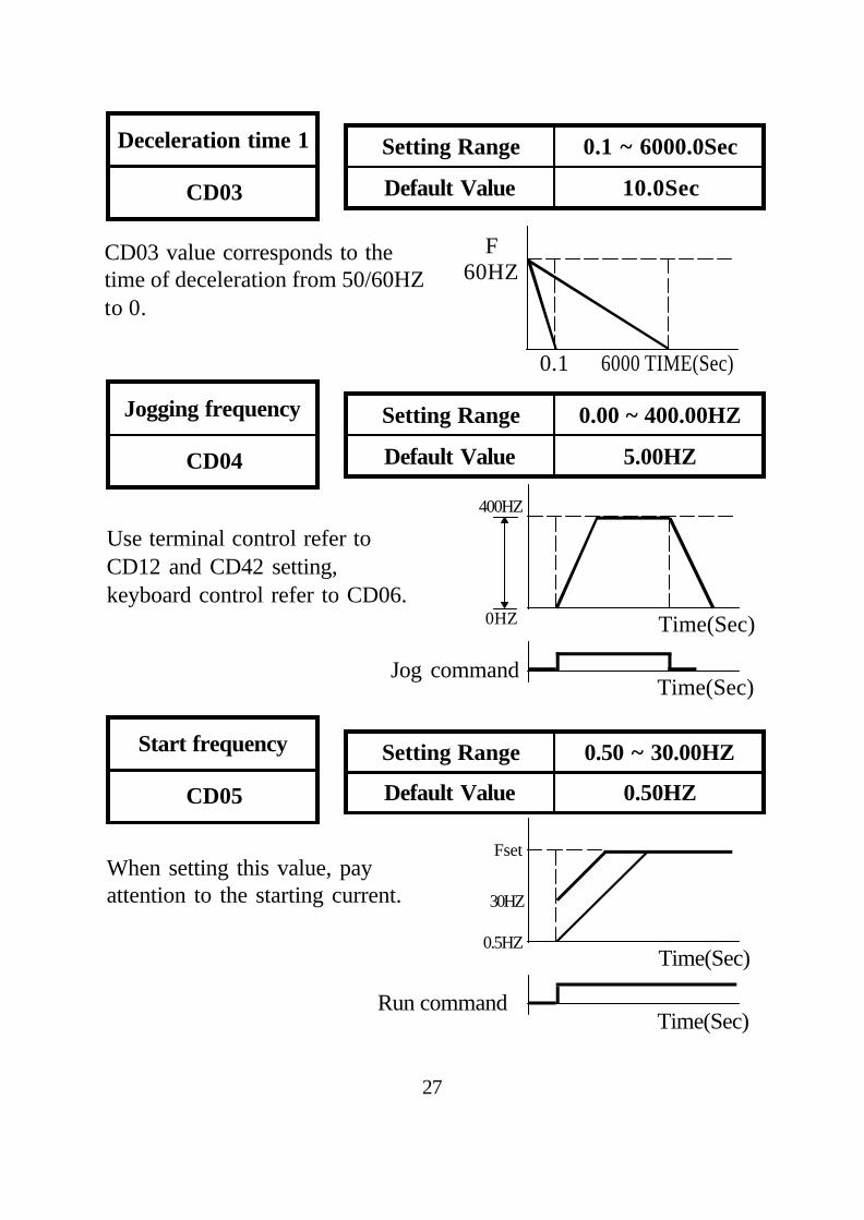
CD03 value corresponds to thetime of deceleration from 50/60HZto 0.
F60HZ
0.1 6000 TIME(Sec)
Use terminal control refer toCD12 and CD42 setting,keyboard control refer to CD06.
Time(Sec)
Jog commandTime(Sec)
400HZ
0HZ
When setting this value, payattention to the starting current.
Time(Sec)
Run commandTime(Sec)
Fset
30HZ
0.5HZ
Deceleration time 1
CD03
Jogging frequency
CD04
Start frequency
CD05
27
Setting Range 0.1 ~ 6000.0Sec
Default Value 10.0Sec
Setting Range 0.00 ~ 400.00HZ
Default Value 5.00HZ
Setting Range 0.50 ~ 30.00HZ
Default Value 0.50HZ
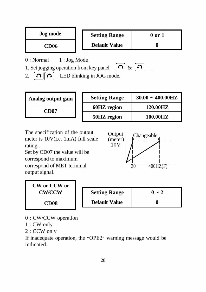
0 : Normal 1 : Jog Mode1. Set jogging operation from key panel & .2. LED blinking in JOG mode.
The specification of the outputmeter is 10V(i.e. 1mA) full scalerating .Set by CD07 the value will becorrespond to maximumcorrespond of MET terminaloutput signal.
0 : CW/CCW operation1 : CW only2 : CCW onlyIf inadequate operation, the “OPE2“ warning message would beindicated.
Jog mode
CD06
CW or CCW orCW/CCW
CD08
Output(meter) 10V
30 400HZ(F)
Changeable
28
Analog output gain
CD07
Setting Range 0 or 1
Default Value 0
Setting Range 0 ~ 2
Default Value 0
Setting Range 30.00 ~ 400.00HZ
60HZ region 120.00HZ
50HZ region 100.00HZ
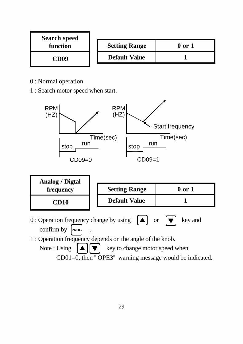
Search speedfunction
CD09
0 : Normal operation.1 : Search motor speed when start.
Analog / Digtalfrequency
CD10
0 : Operation frequency change by using or key and confirm by .1 : Operation frequency depends on the angle of the knob. Note : Using key to change motor speed when CD01=0, then ”OPE3” warning message would be indicated.
29
RPM
stop
(HZ)
Time(sec)
(HZ)RPM
Start frequency
CD09=0 CD09=1
run stop runTime(sec)
PROG
Setting Range 0 or 1
Default Value 1
Setting Range 0 or 1
Default Value 1
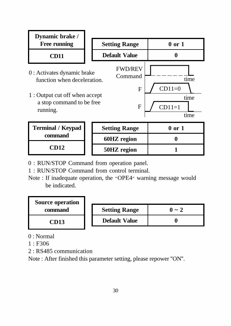
Dynamic brake /Free running
CD11
0 : Activates dynamic brake function when deceleration.
1 : Output cut off when accept a stop command to be free running.
0 : RUN/STOP Command from operation panel.1 : RUN/STOP Command from control terminal.Note : If inadequate operation, the “OPE4“ warning message would be indicated.
CD11=1
CD11=0
FWD/REVCommand time
time
time
F
F
30
0 : Normal1 : F3062 : RS485 communicationNote : After finished this parameter setting, please repower “ON“.
Setting Range 0 or 1
Default Value 0
Setting Range 0 ~ 2
Default Value 0
Source operationcommand
CD13
Terminal / Keypadcommand
CD12
Setting Range 0 or 1
60HZ region 0
50HZ region 1
Max F400HZ
Speed command0.5HZ
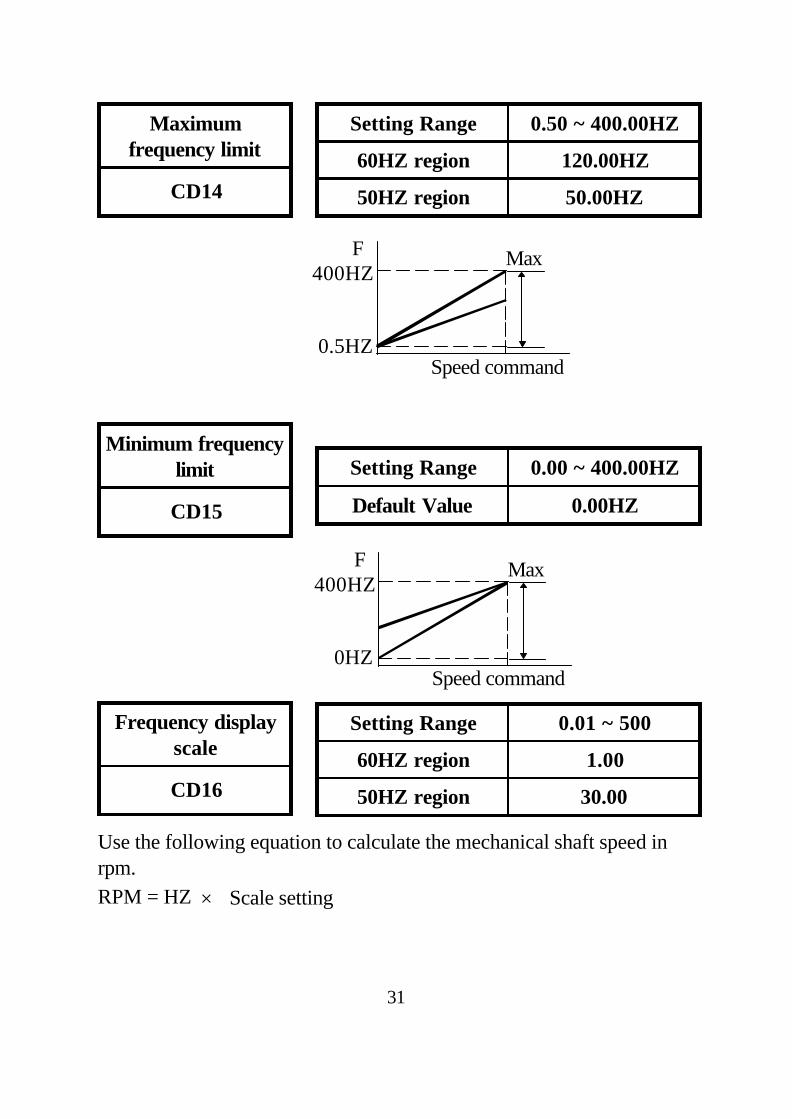
Minimum frequencylimit
CD15
Max F400HZ
Speed command 0HZ
Frequency displayscale
CD16
Use the following equation to calculate the mechanical shaft speed inrpm.
31
Maximumfrequency limit
CD14
Setting Range 0.00 ~ 400.00HZ
Default Value 0.00HZ
Setting Range 0.50 ~ 400.00HZ
60HZ region 120.00HZ
50HZ region 50.00HZ
Setting Range 0.01 ~ 500
60HZ region 1.00
50HZ region 30.00
RPM = HZ Scale setting×
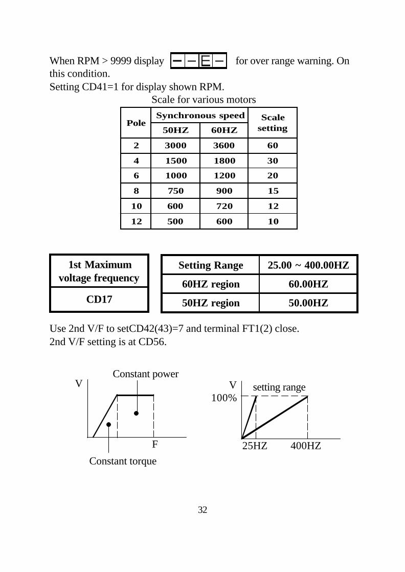
When RPM > 9999 display for over range warning. Onthis condition.Setting CD41=1 for display shown RPM. Scale for various motors
32
PoleSynchronous speed Scale
setting50HZ 60HZ
2 3000 3600 60
4 1500 1800 30
6 1000 1200 20
8 750 900 15
10 600 720 12
12 500 600 10
Use 2nd V/F to setCD42(43)=7 and terminal FT1(2) close.2nd V/F setting is at CD56.
1st Maximumvoltage frequency
CD17
V 100%
25HZ 400HZ
setting range V
F
Constant power
Constant torque
Setting Range 25.00 ~ 400.00HZ
60HZ region 60.00HZ
50HZ region 50.00HZ
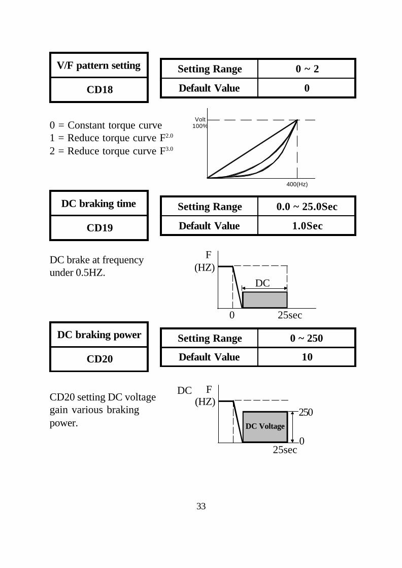
0 = Constant torque curve1 = Reduce torque curve F2.0
2 = Reduce torque curve F3.0
400(Hz)
Volt100%
33
DC braking time
CD19
DC brake at frequencyunder 0.5HZ.
F (HZ)
0 25sec
DC
DC braking power
CD20
CD20 setting DC voltagegain various brakingpower.
F (HZ)
25sec
DC Voltage
DC
250
0
V/F pattern setting
CD18
Setting Range 0 ~ 2
Default Value 0
Setting Range 0.0 ~ 25.0Sec
Default Value 1.0Sec
Setting Range 0 ~ 250
Default Value 10
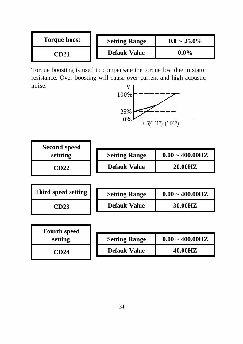
Torque boost
CD21
Torque boosting is used to compensate the torque lost due to statorresistance. Over boosting will cause over current and high acousticnoise. V
100%
0.5(CD17) (CD17)
25%0%
34
Second speedsettting
CD22
Third speed setting
CD23
Fourth speedsetting
CD24
Setting Range 0.0 ~ 25.0%
Default Value 0.0%
Setting Range 0.00 ~ 400.00HZ
Default Value 20.00HZ
Setting Range 0.00 ~ 400.00HZ
Default Value 30.00HZ
Setting Range 0.00 ~ 400.00HZ
Default Value 40.00HZ
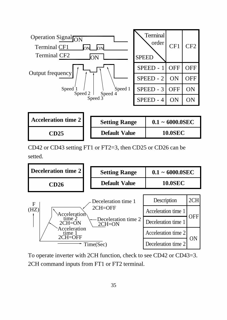
Acceleration time 2
CD25
35
Terminalorder
SPEED
CF1 CF2
SPEED - 1 OFF OFF
SPEED - 2 ON OFF
SPEED - 3 OFF ON
SPEED - 4 ON ON
ONON ON
ON
Operation Signal
Output frequency
Terminal CF1Terminal CF2
Speed 1Speed 2
Speed 3Speed 4
Speed 1
CD42 or CD43 setting FT1 or FT2=3, then CD25 or CD26 can besetted.
Deceleration time 2
CD26
Accelerationtime 2
Accelerationtime 1
Time(Sec)
Deceleration time 1
Deceleration time 2
2CH=OFF
2CH=ON2CH=ON
2CH=OFF
F(HZ)
Description 2CH
Acceleration time 1OFF
Deceleration time 1
Acceleration time 2ON
Deceleration time 2
To operate inverter with 2CH function, check to see CD42 or CD43=3.2CH command inputs from FT1 or FT2 terminal.
Setting Range 0.1 ~ 6000.0SEC
Default Value 10.0SEC
Setting Range 0.1 ~ 6000.0SEC
Default Value 10.0SEC
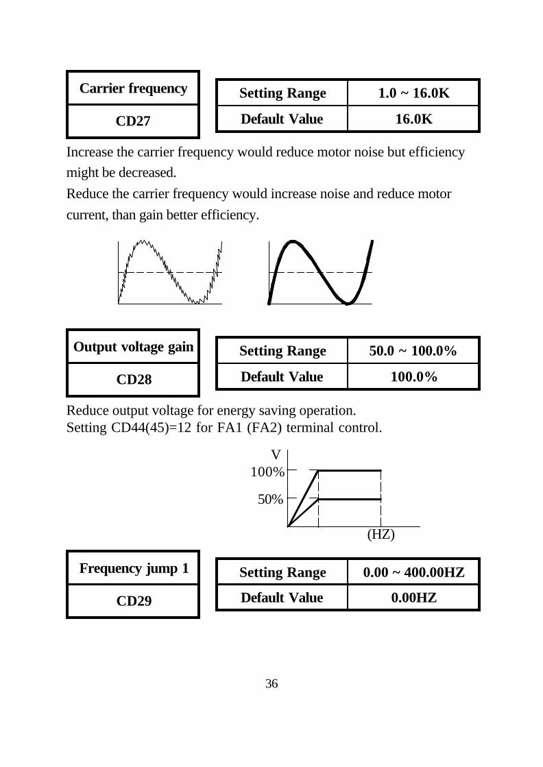
Carrier frequency
CD27
Increase the carrier frequency would reduce motor noise but efficiencymight be decreased.Reduce the carrier frequency would increase noise and reduce motorcurrent, than gain better efficiency.
36
Output voltage gain
CD28
Reduce output voltage for energy saving operation.Setting CD44(45)=12 for FA1 (FA2) terminal control.
Frequency jump 1
CD29
V 100%
50%
(HZ)
Setting Range 1.0 ~ 16.0K
Default Value 16.0K
Setting Range 50.0 ~ 100.0%
Default Value 100.0%
Setting Range 0.00 ~ 400.00HZ
Default Value 0.00HZ
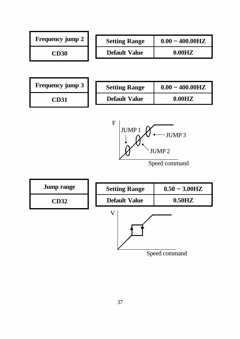
Frequency jump 3
CD31
F
Speed command
JUMP 3
JUMP 2
JUMP 1
37
Frequency jump 2
CD30
Jump range
CD32
V
Speed command
Setting Range 0.00 ~ 400.00HZ
Default Value 0.00HZ
Setting Range 0.00 ~ 400.00HZ
Default Value 0.00HZ
Setting Range 0.50 ~ 3.00HZ
Default Value 0.50HZ
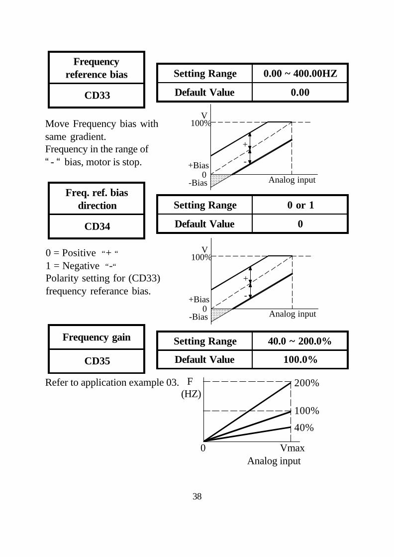
Frequencyreference bias
CD33
Move Frequency bias withsame gradient.Frequency in the range of“- “ bias, motor is stop.
Freq. ref. biasdirection
CD34
0 = Positive “+ “1 = Negative “-“
Polarity setting for (CD33)frequency referance bias.
38
Analog input
V100%
+
-+Bias
-Bias0
Analog input
V100%
+
-+Bias
-Bias0
Frequency gain
CD35
Refer to application example 03. F (HZ)
0 Vmax Analog input
200%
100%
40%
Setting Range 0.00 ~ 400.00HZ
Default Value 0.00
Setting Range 0 or 1
Default Value 0
Setting Range 40.0 ~ 200.0%
Default Value 100.0%
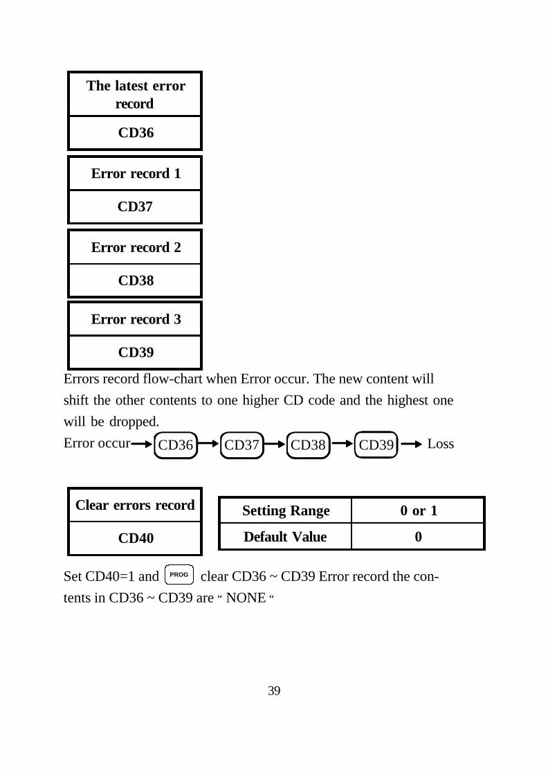
The latest errorrecord
CD36
Error record 1
CD37
Error record 2
CD38
39
Error record 3
CD39
Errors record flow-chart when Error occur. The new content willshift the other contents to one higher CD code and the highest onewill be dropped.Error occur LossCD36 CD37 CD38 CD39
Clear errors record
CD40
Set CD40=1 and clear CD36 ~ CD39 Error record the con-tents in CD36 ~ CD39 are “ NONE “
PROG
Setting Range 0 or 1
Default Value 0
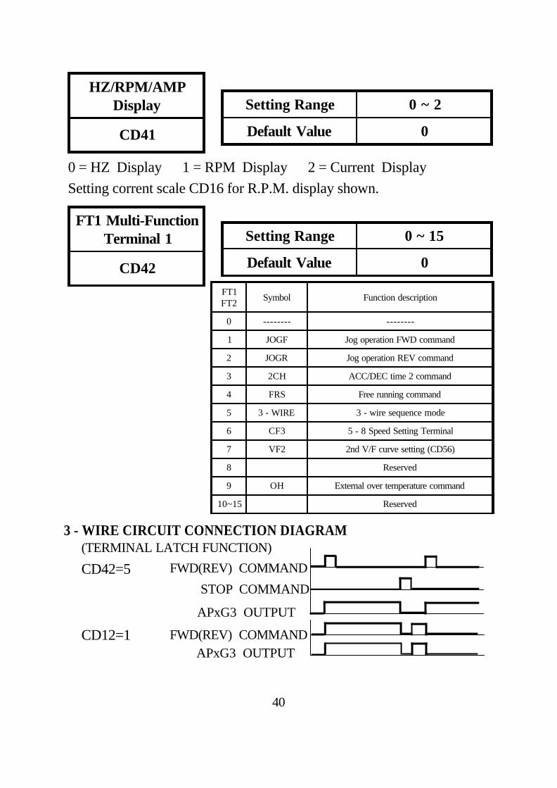
0 = HZ Display 1 = RPM Display 2 = Current DisplaySetting corrent scale CD16 for R.P.M. display shown.
40
FT1 Multi-FunctionTerminal 1
CD42
3 - WIRE CIRCUIT CONNECTION DIAGRAM
CD42=5
CD12=1
STOP COMMAND
APxG3 OUTPUT
FWD(REV) COMMANDAPxG3 OUTPUT
FWD(REV) COMMAND
(TERMINAL LATCH FUNCTION)
HZ/RPM/AMPDisplay
CD41
Setting Range 0 ~ 2
Default Value 0
Setting Range 0 ~ 15
Default Value 0
FT1FT2 Symbol Function description
0 -------- --------
1 JOGF Jog operation FWD command
2 JOGR Jog operation REV command
3 2CH ACC/DEC time 2 command
4 FRS Free running command
5 3 - WIRE 3 - wire sequence mode
6 CF3 5 - 8 Speed Setting Terminal
7 VF2 2nd V/F curve setting (CD56)
8 Reserved
9 OH External over temperature command
10~15 Reserved
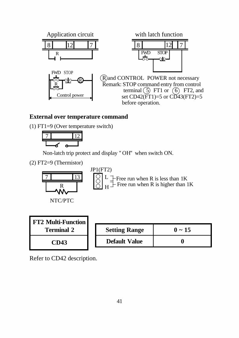
41
with latch function
R and CONTROL POWER not necessaryRemark: STOP command entry from control terminal 5 FT1 or 6 FT2, and set CD42(FT1)=5 or CD43(FT2)=5 before operation.
12 78
Application circuit
R
12 78FWD STOP
Control power
FWD STOP
RR
External over temperature command(1) FT1=9 (Over temperature switch)
Non-latch trip protect and display “OH“ when switch ON.
(2) FT2=9 (Thermistor)
ΩΩ
7 12
7 13
NTC/PTC
R Free run when R is higher than 1KFree run when R is less than 1KL
H
JP1(FT2)
FT2 Multi-FunctionTerminal 2
CD43
Refer to CD42 description.
Setting Range 0 ~ 15
Default Value 0
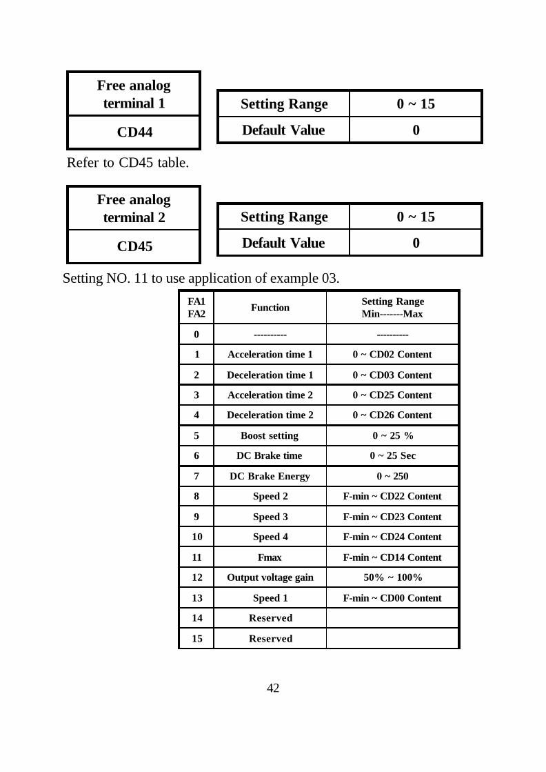
Free analogterminal 1
CD44
Refer to CD45 table.
Free analogterminal 2
CD45
Setting NO. 11 to use application of example 03.
42
Setting Range 0 ~ 15
Default Value 0
Setting Range 0 ~ 15
Default Value 0
FA1FA2 Function Setting Range
Min-------Max
0 ---------- ----------
1 Acceleration time 1 0 ~ CD02 Content
2 Deceleration time 1 0 ~ CD03 Content
3 Acceleration time 2 0 ~ CD25 Content
4 Deceleration time 2 0 ~ CD26 Content
5 Boost setting 0 ~ 25 %
6 DC Brake time 0 ~ 25 Sec
7 DC Brake Energy 0 ~ 250
8 Speed 2 F-min ~ CD22 Content
9 Speed 3 F-min ~ CD23 Content
10 Speed 4 F-min ~ CD24 Content
11 Fmax F-min ~ CD14 Content
12 Output voltage gain 50% ~ 100%
13 Speed 1 F-min ~ CD00 Content
14 Reserved
15 Reserved
5th speed setting
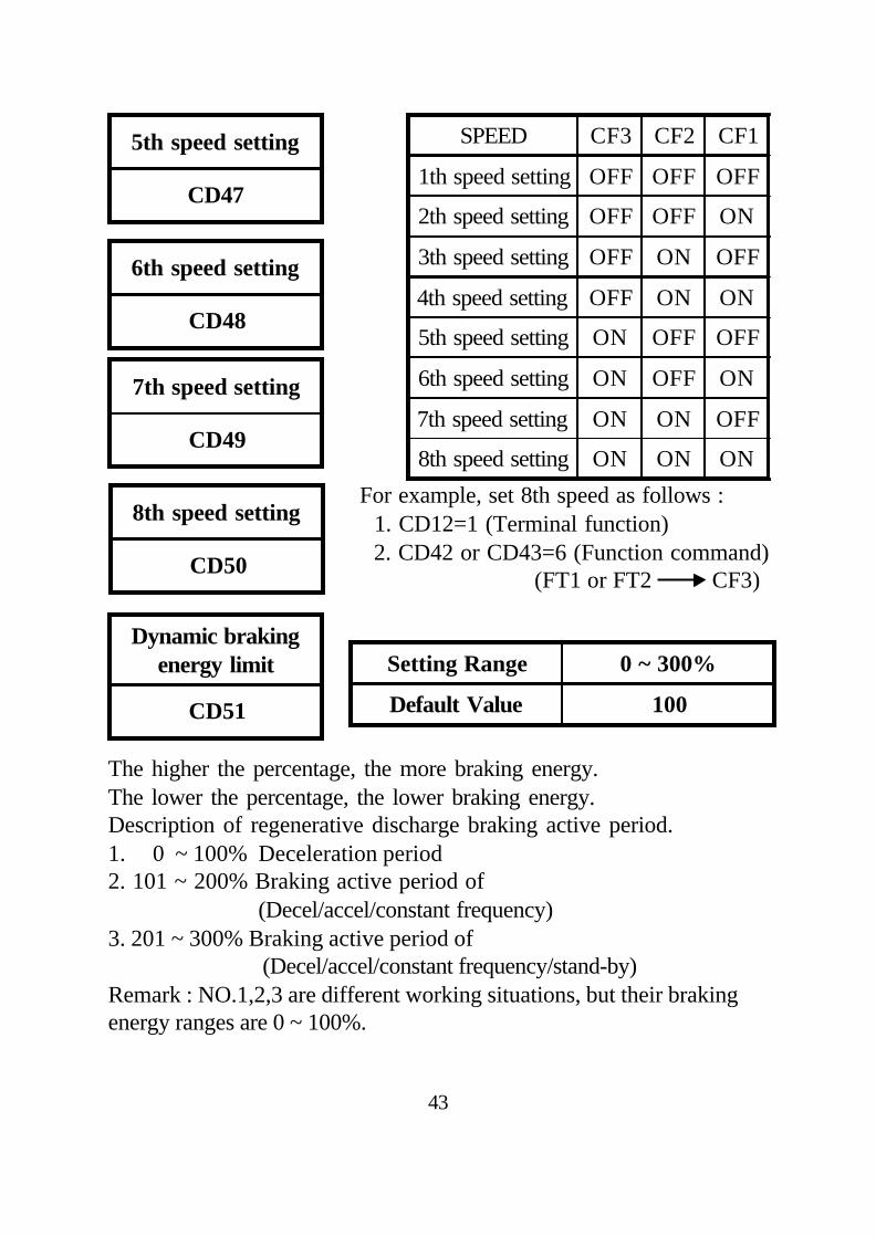
CD47
6th speed setting
CD48
7th speed setting
CD49
8th speed setting
CD50
Dynamic brakingenergy limit
CD51
The higher the percentage, the more braking energy.The lower the percentage, the lower braking energy.Description of regenerative discharge braking active period.1. 0 ~ 100% Deceleration period2. 101 ~ 200% Braking active period of (Decel/accel/constant frequency)3. 201 ~ 300% Braking active period of (Decel/accel/constant frequency/stand-by)Remark : NO.1,2,3 are different working situations, but their brakingenergy ranges are 0 ~ 100%.
SPEED CF3 CF2 CF1
1th speed setting OFF OFF OFF
2th speed setting OFF OFF ON
3th speed setting OFF ON OFF
4th speed setting OFF ON ON
5th speed setting ON OFF OFF
6th speed setting ON OFF ON
7th speed setting ON ON OFF
8th speed setting ON ON ON
For example, set 8th speed as follows : 1. CD12=1 (Terminal function) 2. CD42 or CD43=6 (Function command) (FT1 or FT2 CF3)
43
Setting Range 0 ~ 300%
Default Value 100
Version selector
CD52
Select function CD52, then use UP/Down key to select F50.0/F60.0Version. Press to save it. System will return to the factorysetting and go into waiting mode..
S curve
CD53
Setting S curve non-Linear Accel/Decel Operation from 1 to 10.Setting 0 is normal operation without S curve.
44
FWD RUN COMMAND
Output Frequency
ACCEL DECELBraking TimeDC injection
S Curve period
REV RUN COMMAND
PROG
CD53=0CD53=3CD53=7
F(Hz)
TIME
Setting Range 0 ~ 10
Default Value 0
Setting Range F50.0/F60.0
60HZ region F60.0
50HZ region F50.0
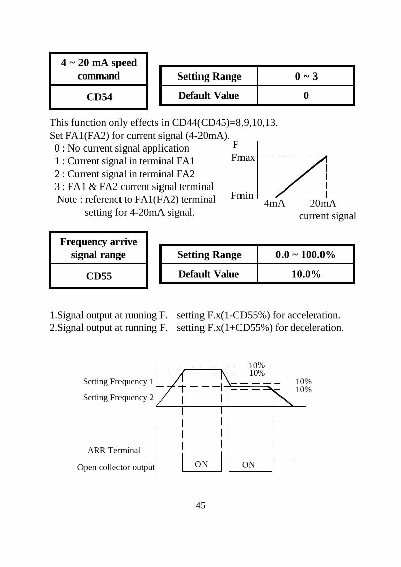
This function only effects in CD44(CD45)=8,9,10,13.Set FA1(FA2) for current signal (4-20mA). 0 : No current signal application 1 : Current signal in terminal FA1 2 : Current signal in terminal FA2 3 : FA1 & FA2 current signal terminal Note : referenct to FA1(FA2) terminal setting for 4-20mA signal.
F Fmax
Fmin4mA 20mA current signal
Frequency arrivesignal range
CD55
1.Signal output at running F.≧ setting F.x(1-CD55%) for acceleration.2.Signal output at running F.≦ setting F.x(1+CD55%) for deceleration.
45
+10%-10%
-10%+10%
ON ON
Setting Frequency 1
Setting Frequency 2
ARR Terminal
Open collector output
4 ~ 20 mA speedcommand
CD54
Setting Range 0 ~ 3
Default Value 0
Setting Range 0.0 ~ 100.0%
Default Value 10.0%
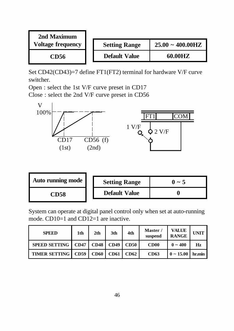
2nd MaximumVoltage frequency
CD56
Set CD42(CD43)=7 define FT1(FT2) terminal for hardware V/F curveswitcher.Open : select the 1st V/F curve preset in CD17Close : select the 2nd V/F curve preset in CD56
V 100%
CD17 CD56 (f) (1st) (2nd)
FT1 COM
2 V/F1 V/F
46
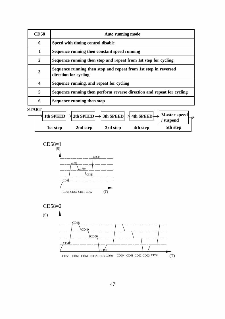
Auto running mode
CD58
System can operate at digital panel control only when set at auto-runningmode. CD10=1 and CD12=1 are inactive.
Setting Range 25.00 ~ 400.00HZ
Default Value 60.00HZ
Setting Range 0 ~ 5
Default Value 0
SPEED 1th 2th 3th 4th Master /suspend
VALUERANGE
UNIT
SPEED SETTING CD47 CD48 CD49 CD50 CD00 0 ~ 400 Hz
TIMER SETTING CD59 CD60 CD61 CD62 CD63 0 ~ 15.00 hr.min
47
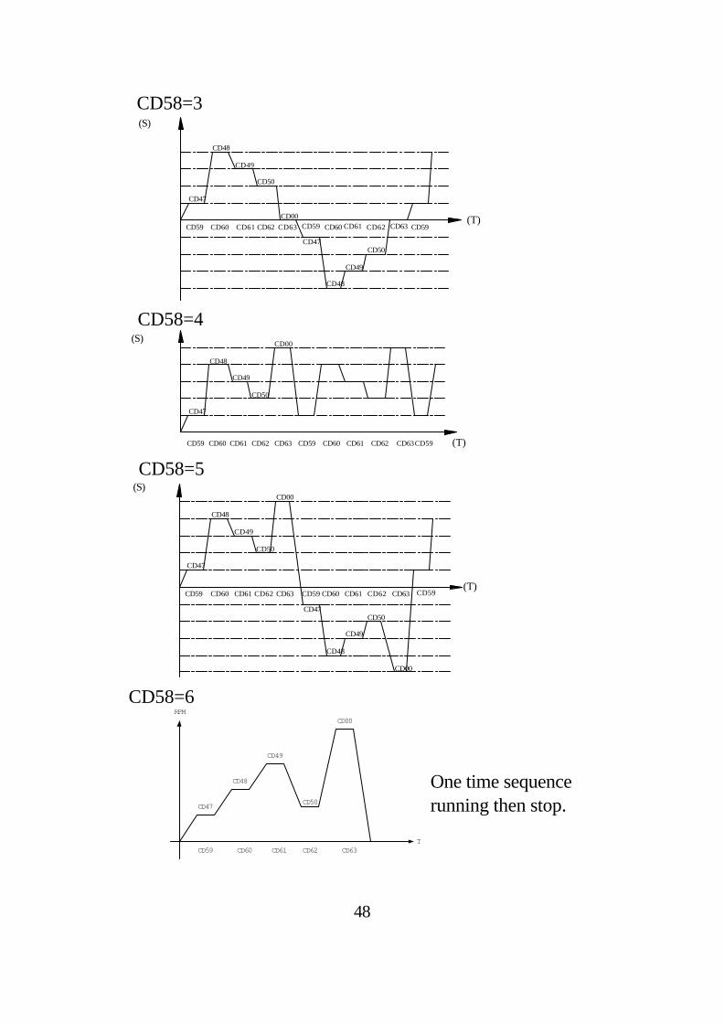
CD58 Auto running mode
0 Speed with timing control disable
1 Sequence running then constant speed running
2 Sequence running then stop and repeat from 1st step for cycling
3Sequence running then stop and repeat from 1st step in reverseddirection for cycling
4 Sequence running, and repeat for cycling
5 Sequence running then perform reverse direction and repeat for cycling
6 Sequence running then stop
CD59 CD60 CD61 CD62 (T)
(S)
CD47
CD48
CD49
CD00
CD50
CD58=1
CD58=2
CD61CD60CD59 (T)CD62 CD63 CD59 CD60 CD61 CD63CD62 CD59
(S)
CD48
CD49
CD50
CD47
CD00
STARTMaster speed/ suspend
1th SPEED 3th SPEED2th SPEED 4th SPEED
1st step 2nd step 4th step 5th step3rd step
48
CD47
CD48
CD49
CD50
CD00
CD59 CD60 CD61CD62 CD63T
RPM
CD58=3
CD59CD59
(S)
CD59CD62CD61CD60 CD63 CD62CD61CD60 CD63 (T)
CD47
CD48
CD49
CD50
CD00
CD59 CD61CD63CD61CD60 CD62 CD59 CD60 CD62 CD63(T)
CD59
(S)
CD47
CD48
CD49
CD50
CD00
CD48
CD47
CD49
CD50
CD59CD63CD62CD61CD60CD59 CD63CD60CD59 CD62CD61(T)
(S)
CD47
CD48
CD49
CD50
CD00
CD48
CD49
CD50
CD00
CD47
CD58=4
CD58=5
CD58=6
One time sequencerunning then stop.
49
Setting running time for 2th speed.(CD48)
2st step timer
CD60
Setting running time for 3th speed.(CD49)
3st step timer
CD61
Setting running time for 4th speed.(CD50)
4st step timer
CD62
Setting running time for 1th speed.(CD00)
5st step timer
CD63
1st step timer
CD59
Setting running time for 1th speed.(CD47)
Setting Range 0 ~ 15Hr
Default Value 0.01Hr.min
Setting Range 0 ~ 15Hr
Default Value 0.00Hr.min
Setting Range 0 ~ 15Hr
Default Value 0.00Hr.min
Setting Range 0 ~ 15Hr
Default Value 0.00Hr.min
Setting Range 0 ~ 15Hr
Default Value 0.00Hr.min
50
Stall prevention
CD65
0 : Disable1 : EnableWhen enable CD65, if any overload over CD66 setting value duringDEC period, inverter will increase DEC time to prevent inverter to gointo fail safe mode.
Overload currentstall prevention
CD66
During ACC, if ACC time is tooshort or load is too heavy, thecurrent will reach CD66 value,inverter will stop to ACC untilcurrent is lower than CD66value.
CD66
Time
Output HZ
Constant frequency
Current
Actual stall current limit=rate current × CD66 percentage. Rate currentnumber refers to section 2 table.
0 : hr.min1 : min.secNote 1 : CD64 cannot be reset to default value by CD52. Set CD64 as needs separately.Note 2 : In RS485 communication input, CD59~CD63 need to tranfer minimum unit. Ex CD64=0, CD59=2.3 CD59 contant for RS485 communication is 2 × 60+30=150(0096H).
Timer unit selector
CD64
Setting Range 0 ~ 1
Default Value 0
Setting Range 0 ~ 1
Default Value 0
Setting Range 20 ~ 250%
Default Value 170%
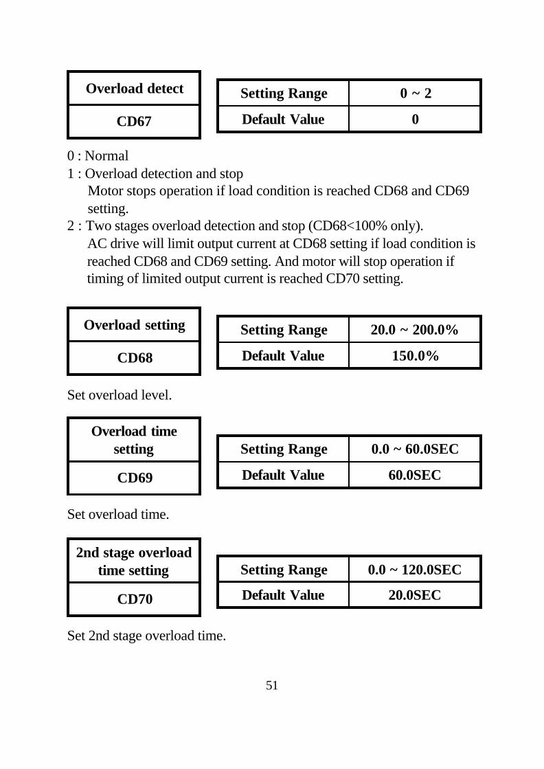
Overload detect
CD67
0 : Normal1 : Overload detection and stop Motor stops operation if load condition is reached CD68 and CD69 setting.2 : Two stages overload detection and stop (CD68<100% only). AC drive will limit output current at CD68 setting if load condition is reached CD68 and CD69 setting. And motor will stop operation if timing of limited output current is reached CD70 setting.
Overload setting
CD68
Set overload level.
Overload timesetting
CD69
Set overload time.
2nd stage overloadtime setting
CD70
Set 2nd stage overload time.
51
Setting Range 0 ~ 2
Default Value 0
Setting Range 20.0 ~ 200.0%
Default Value 150.0%
Setting Range 0.0 ~ 60.0SEC
Default Value 60.0SEC
Setting Range 0.0 ~ 120.0SEC
Default Value 20.0SEC
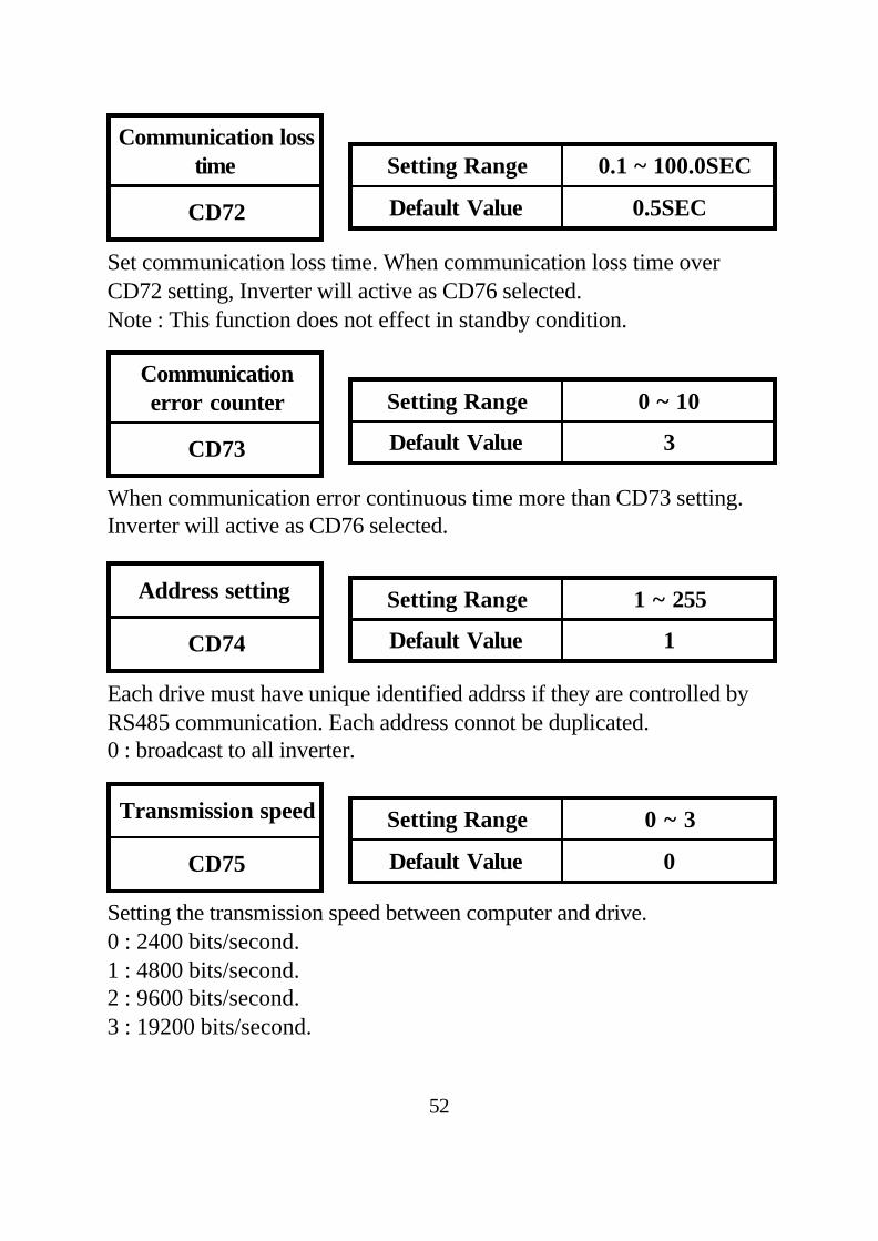
Communication losstime
CD72
Setting Range 0.1 ~ 100.0SEC
Default Value 0.5SEC
Set communication loss time. When communication loss time overCD72 setting, Inverter will active as CD76 selected.Note : This function does not effect in standby condition.
Communicationerror counter
CD73
Setting Range 0 ~ 10
Default Value 3
When communication error continuous time more than CD73 setting.Inverter will active as CD76 selected.
Address setting
CD74
Each drive must have unique identified addrss if they are controlled byRS485 communication. Each address connot be duplicated.0 : broadcast to all inverter.
Setting Range 1 ~ 255
Default Value 1
Transmission speed
CD75
Setting the transmission speed between computer and drive.0 : 2400 bits/second.1 : 4800 bits/second.2 : 9600 bits/second.3 : 19200 bits/second.
Setting Range 0 ~ 3
Default Value 0
52
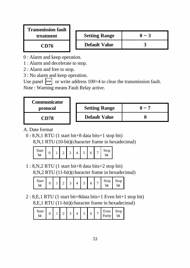
53
Transmission faulttreatment
CD76
0 : Alarm and keep operation.1 : Alarm and decelerate to stop.2 : Alarm and free to stop.3 : No alarm and keep operation.Use panel or write address 100=4 to clear the transmission fault.Note : Warning means Fault Relay active.
Setting Range 0 ~ 3
Default Value 3
Communicatorprotocol
CD78
A. Date format 0 : 8,N,1 RTU (1 start bit+8 data bits+1 stop bit) 8,N,1 RTU (10-bit)(character frame in hexadecimal)
1 : 8,N,2 RTU (1 start bit+8 data bits+2 stop bit) 8,N,2 RTU (11-bit)(character frame in hexadecimal)
2 : 8,E,1 RTU (1 start bit+8data bits+1 Even bit+1 stop bit) 8,E,1 RTU (11-bit)(character frame in hexadecimal)
Startbit 0 1 2 3 4 5 6 7
Stopbit
Startbit 0 1 2 3 4 5 6 7
Stopbit
Stopbit
Startbit 0 1 2 3 4 5 6 7
EvenParity
Stopbit
Setting Range 0 ~ 7
Default Value 0
STOP
54
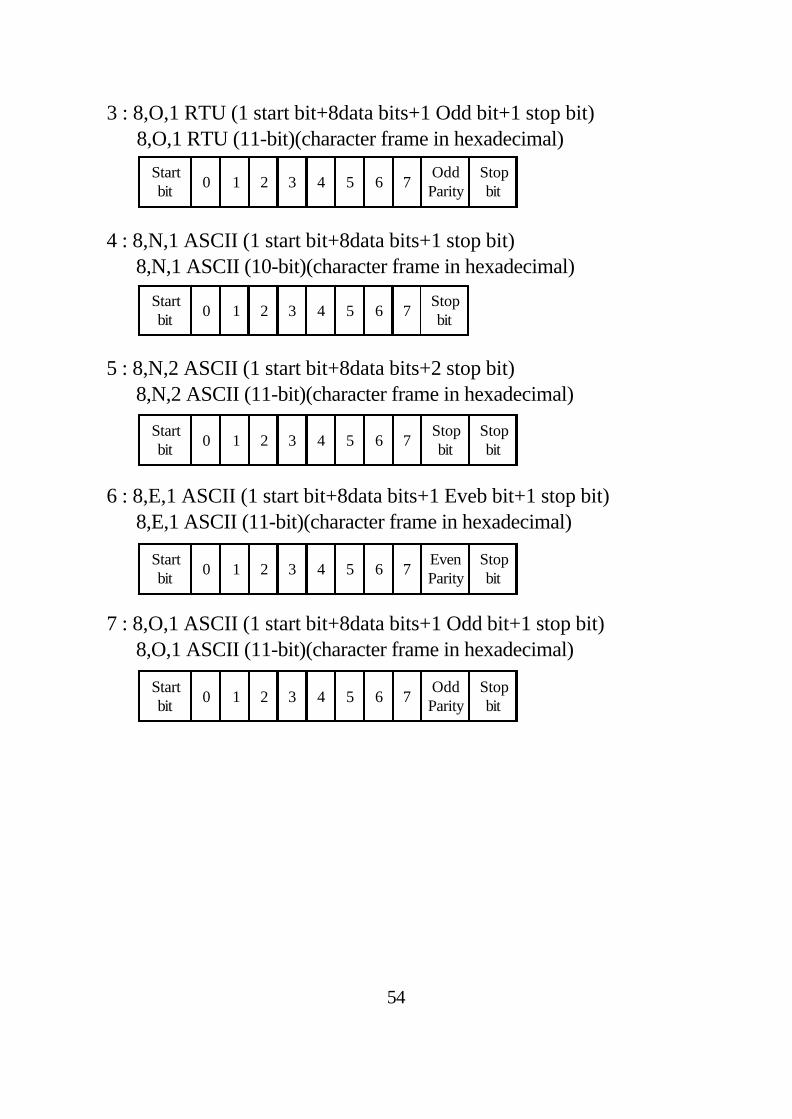
3 : 8,O,1 RTU (1 start bit+8data bits+1 Odd bit+1 stop bit) 8,O,1 RTU (11-bit)(character frame in hexadecimal)
4 : 8,N,1 ASCII (1 start bit+8data bits+1 stop bit) 8,N,1 ASCII (10-bit)(character frame in hexadecimal)
5 : 8,N,2 ASCII (1 start bit+8data bits+2 stop bit) 8,N,2 ASCII (11-bit)(character frame in hexadecimal)
6 : 8,E,1 ASCII (1 start bit+8data bits+1 Eveb bit+1 stop bit) 8,E,1 ASCII (11-bit)(character frame in hexadecimal)
7 : 8,O,1 ASCII (1 start bit+8data bits+1 Odd bit+1 stop bit) 8,O,1 ASCII (11-bit)(character frame in hexadecimal)
Startbit 0 1 2 3 4 5 6 7
OddParity
Stopbit
Startbit 0 1 2 3 4 5 6 7
Stopbit
Startbit 0 1 2 3 4 5 6 7
Stopbit
Stopbit
Startbit 0 1 2 3 4 5 6 7
EvenParity
Stopbit
Startbit 0 1 2 3 4 5 6 7
OddParity
Stopbit
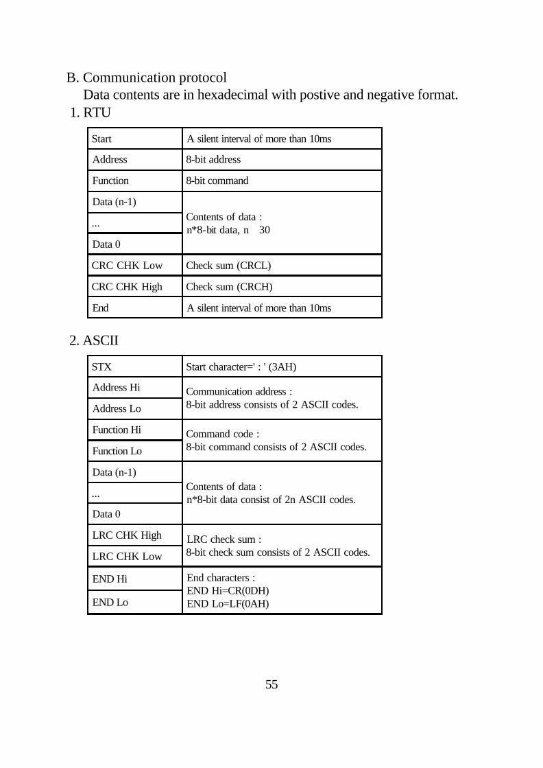
B. Communication protocol Data contents are in hexadecimal with postive and negative format. 1. RTU
2. ASCII
Start A silent interval of more than 10ms
Address 8-bit address
Function 8-bit command
Data (n-1)Contents of data :n*8-bit data, n 30≦
...
Data 0
CRC CHK Low Check sum (CRCL)
CRC CHK High Check sum (CRCH)
End A silent interval of more than 10ms
55
STX Start character=' : ' (3AH)
Address Hi Communication address :8-bit address consists of 2 ASCII codes.Address Lo
Function Hi Command code :8-bit command consists of 2 ASCII codes.Function Lo
Data (n-1)Contents of data :n*8-bit data consist of 2n ASCII codes....
Data 0
LRC CHK High LRC check sum :8-bit check sum consists of 2 ASCII codes.LRC CHK Low
END Hi End characters :END Hi=CR(0DH)END Lo=LF(0AH)END Lo
56
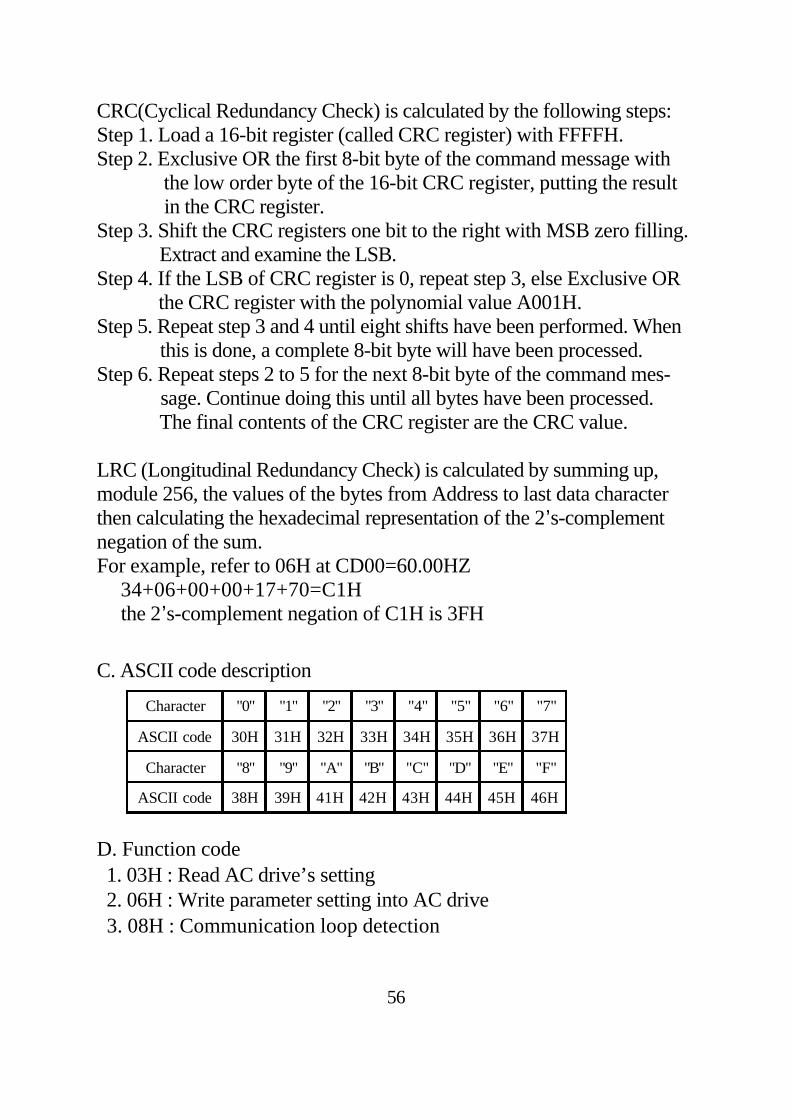
CRC(Cyclical Redundancy Check) is calculated by the following steps:Step 1. Load a 16-bit register (called CRC register) with FFFFH.Step 2. Exclusive OR the first 8-bit byte of the command message with the low order byte of the 16-bit CRC register, putting the result in the CRC register.Step 3. Shift the CRC registers one bit to the right with MSB zero filling. Extract and examine the LSB.Step 4. If the LSB of CRC register is 0, repeat step 3, else Exclusive OR the CRC register with the polynomial value A001H.Step 5. Repeat step 3 and 4 until eight shifts have been performed. When this is done, a complete 8-bit byte will have been processed.Step 6. Repeat steps 2 to 5 for the next 8-bit byte of the command mes- sage. Continue doing this until all bytes have been processed. The final contents of the CRC register are the CRC value.
LRC (Longitudinal Redundancy Check) is calculated by summing up,module 256, the values of the bytes from Address to last data characterthen calculating the hexadecimal representation of the 2’s-complementnegation of the sum.For example, refer to 06H at CD00=60.00HZ 34+06+00+00+17+70=C1H the 2’s-complement negation of C1H is 3FH
C. ASCII code description
D. Function code 1. 03H : Read AC drive’s setting 2. 06H : Write parameter setting into AC drive 3. 08H : Communication loop detection
Character "0" "1" "2" "3" "4" "5" "6" "7"
ASCII code 30H 31H 32H 33H 34H 35H 36H 37H
Character "8" "9" "A" "B" "C" "D" "E" "F"
ASCII code 38H 39H 41H 42H 43H 44H 45H 46H
57
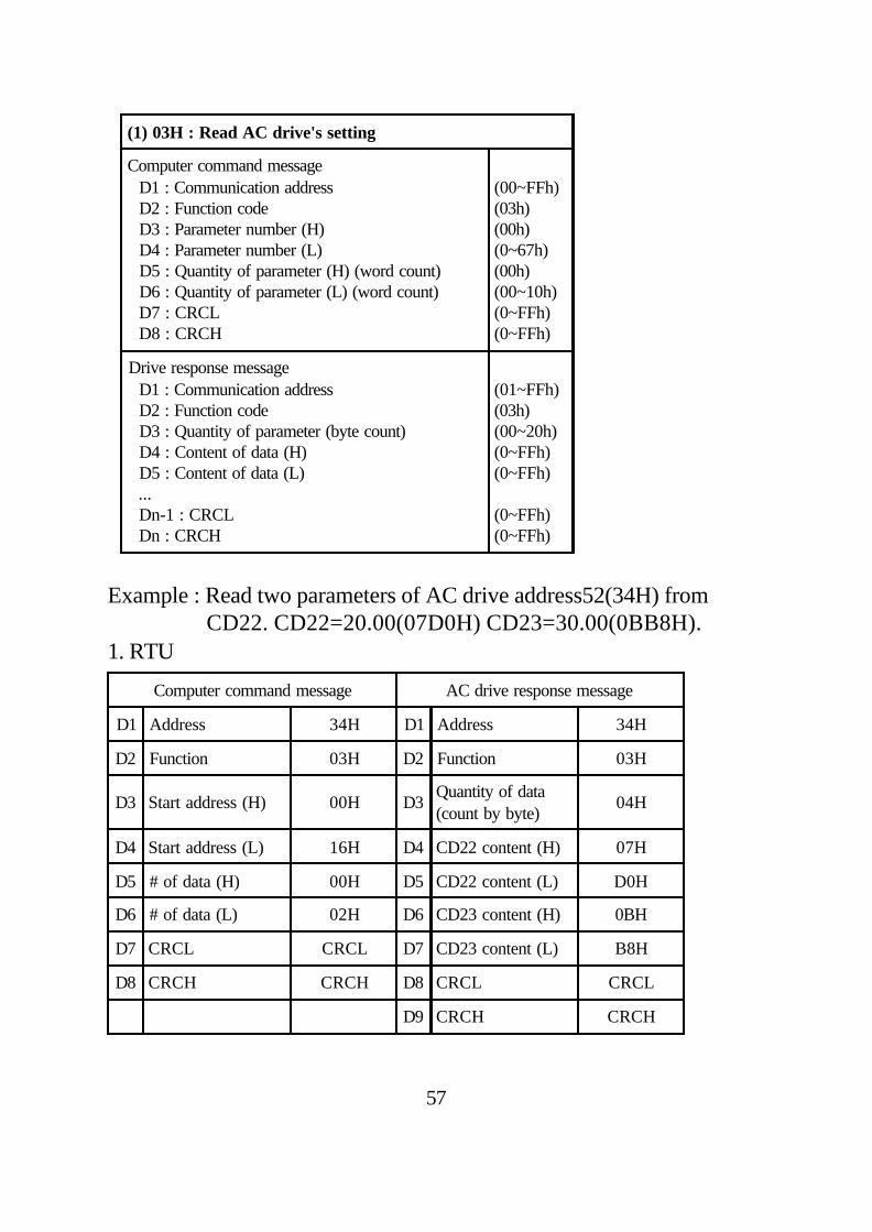
Example : Read two parameters of AC drive address52(34H) from CD22. CD22=20.00(07D0H) CD23=30.00(0BB8H).1. RTU
(1) 03H : Read AC drive's setting
Computer command message D1 : Communication address D2 : Function code D3 : Parameter number (H) D4 : Parameter number (L) D5 : Quantity of parameter (H) (word count) D6 : Quantity of parameter (L) (word count) D7 : CRCL D8 : CRCH
(00~FFh)(03h)(00h)(0~67h)(00h)(00~10h)(0~FFh)(0~FFh)
Drive response message D1 : Communication address D2 : Function code D3 : Quantity of parameter (byte count) D4 : Content of data (H) D5 : Content of data (L) ... Dn-1 : CRCL Dn : CRCH
(01~FFh)(03h)(00~20h)(0~FFh)(0~FFh)
(0~FFh)(0~FFh)
Computer command message AC drive response message
D1 Address 34H D1 Address 34H
D2 Function 03H D2 Function 03H
D3 Start address (H) 00H D3Quantity of data(count by byte)
04H
D4 Start address (L) 16H D4 CD22 content (H) 07H
D5 # of data (H) 00H D5 CD22 content (L) D0H
D6 # of data (L) 02H D6 CD23 content (H) 0BH
D7 CRCL CRCL D7 CD23 content (L) B8H
D8 CRCH CRCH D8 CRCL CRCL
D9 CRCH CRCH
58
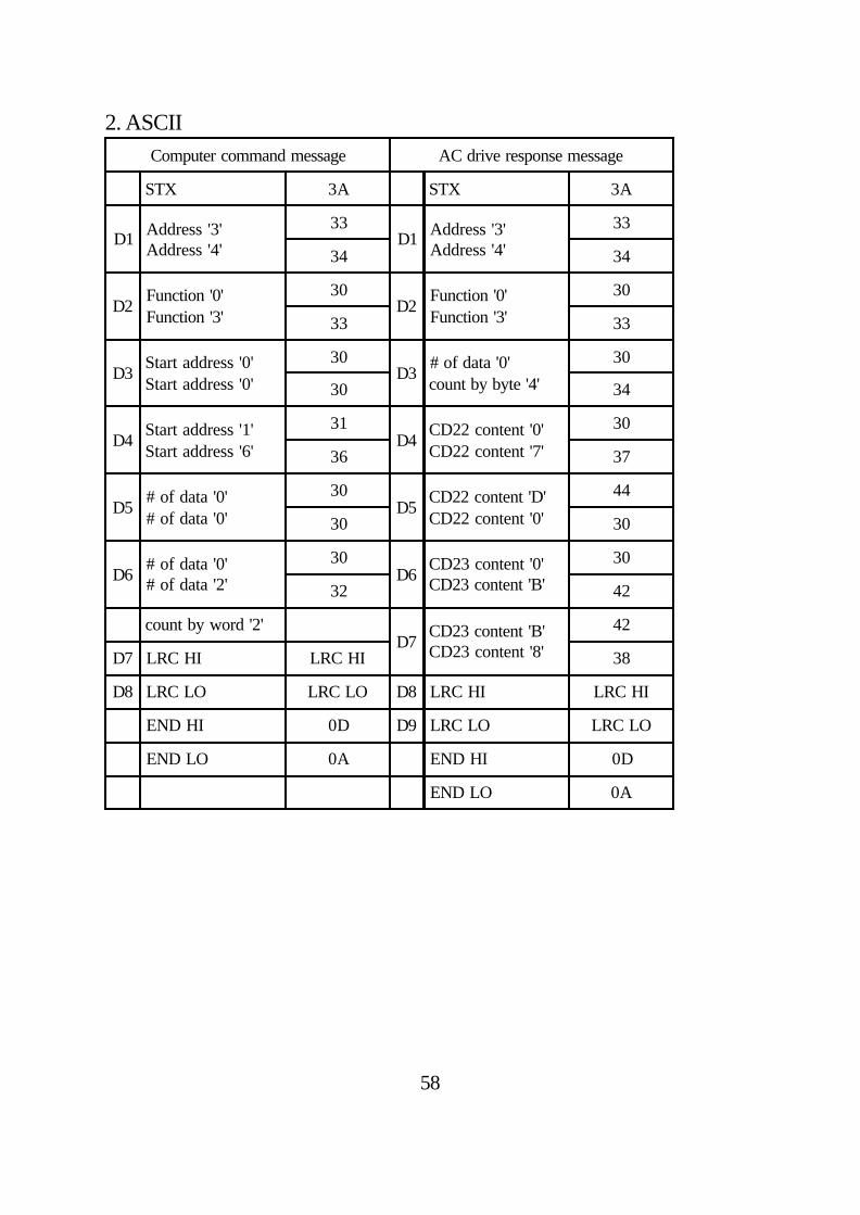
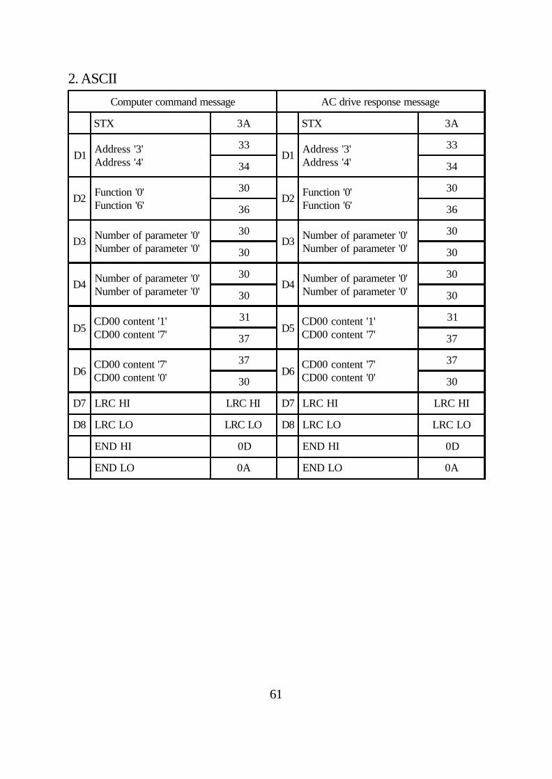
2. ASCIIComputer command message AC drive response message
STX 3A STX 3A
D1 Address '3'Address '4'
33D1 Address '3'
Address '4'
33
34 34
D2Function '0'Function '3'
30D2
Function '0'Function '3'
30
33 33
D3Start address '0'Start address '0'
30D3
# of data '0'count by byte '4'
30
30 34
D4Start address '1'Start address '6'
31D4
CD22 content '0'CD22 content '7'
30
36 37
D5# of data '0'# of data '0'
30D5
CD22 content 'D'CD22 content '0'
44
30 30
D6# of data '0'# of data '2'
30D6
CD23 content '0'CD23 content 'B'
30
32 42
count by word '2'D7
CD23 content 'B'CD23 content '8'
42
D7 LRC HI LRC HI 38
D8 LRC LO LRC LO D8 LRC HI LRC HI
END HI 0D D9 LRC LO LRC LO
END LO 0A END HI 0D
END LO 0A
59
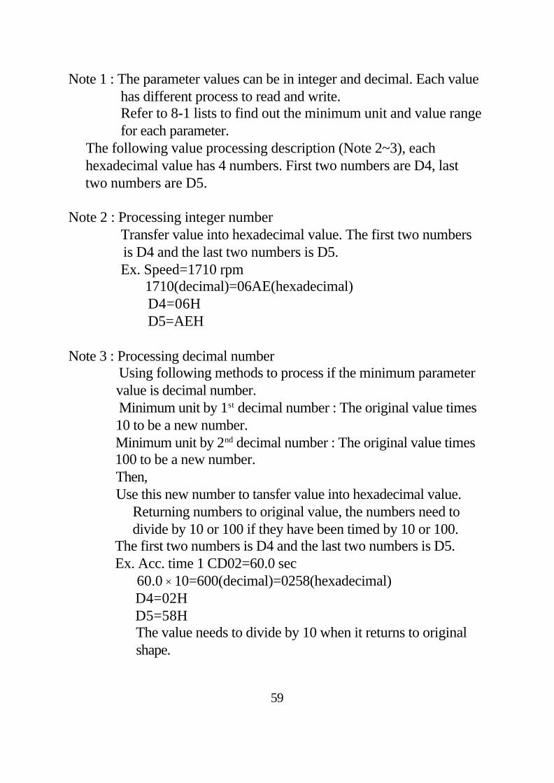
Note 1 : The parameter values can be in integer and decimal. Each value has different process to read and write. Refer to 8-1 lists to find out the minimum unit and value range for each parameter. The following value processing description (Note 2~3), each hexadecimal value has 4 numbers. First two numbers are D4, last two numbers are D5.
Note 2 : Processing integer number Transfer value into hexadecimal value. The first two numbers is D4 and the last two numbers is D5. Ex. Speed=1710 rpm 1710(decimal)=06AE(hexadecimal) D4=06H D5=AEH
Note 3 : Processing decimal number Using following methods to process if the minimum parameter value is decimal number. Minimum unit by 1st decimal number : The original value times 10 to be a new number. Minimum unit by 2nd decimal number : The original value times 100 to be a new number. Then, Use this new number to tansfer value into hexadecimal value. Returning numbers to original value, the numbers need to divide by 10 or 100 if they have been timed by 10 or 100. The first two numbers is D4 and the last two numbers is D5. Ex. Acc. time 1 CD02=60.0 sec 60.0 × 10=600(decimal)=0258(hexadecimal) D4=02H D5=58H The value needs to divide by 10 when it returns to original shape.
※
※
60
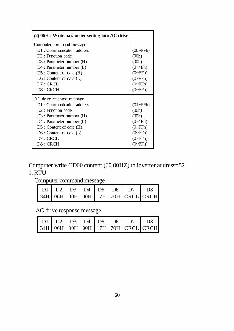
Computer write CD00 content (60.00HZ) to inverter address=521. RTU Computer command message
AC drive response message
D134H
D206H
D300H
D400H
D517H
D670H
D7CRCL
D8CRCH
D134H
D206H
D300H
D400H
D517H
D670H
D7CRCL
D8CRCH
(2) 06H : Write parameter setting into AC drive
Computer command message D1 : Communication address D2 : Function code D3 : Parameter number (H) D4 : Parameter number (L) D5 : Content of data (H) D6 : Content of data (L) D7 : CRCL D8 : CRCH
(00~FFh)(06h)(00h)(0~4Eh)(0~FFh)(0~FFh)(0~FFh)(0~FFh)
AC drive response message D1 : Communication address D2 : Function code D3 : Parameter number (H) D4 : Parameter number (L) D5 : Content of data (H) D6 : Content of data (L) D7 : CRCL D8 : CRCH
(01~FFh)(06h)(00h)(0~4Eh)(0~FFh)(0~FFh)(0~FFh)(0~FFh)
61
2. ASCII
Computer command message AC drive response message
STX 3A STX 3A
D1 Address '3'Address '4'
33D1 Address '3'
Address '4'
33
34 34
D2 Function '0'Function '6'
30D2 Function '0'
Function '6'
30
36 36
D3 Number of parameter '0'Number of parameter '0'
30D3 Number of parameter '0'
Number of parameter '0'
30
30 30
D4 Number of parameter '0'Number of parameter '0'
30D4 Number of parameter '0'
Number of parameter '0'
30
30 30
D5CD00 content '1'CD00 content '7'
31D5
CD00 content '1'CD00 content '7'
31
37 37
D6CD00 content '7'CD00 content '0'
37D6
CD00 content '7'CD00 content '0'
37
30 30
D7 LRC HI LRC HI D7 LRC HI LRC HI
D8 LRC LO LRC LO D8 LRC LO LRC LO
END HI 0D END HI 0D
END LO 0A END LO 0A
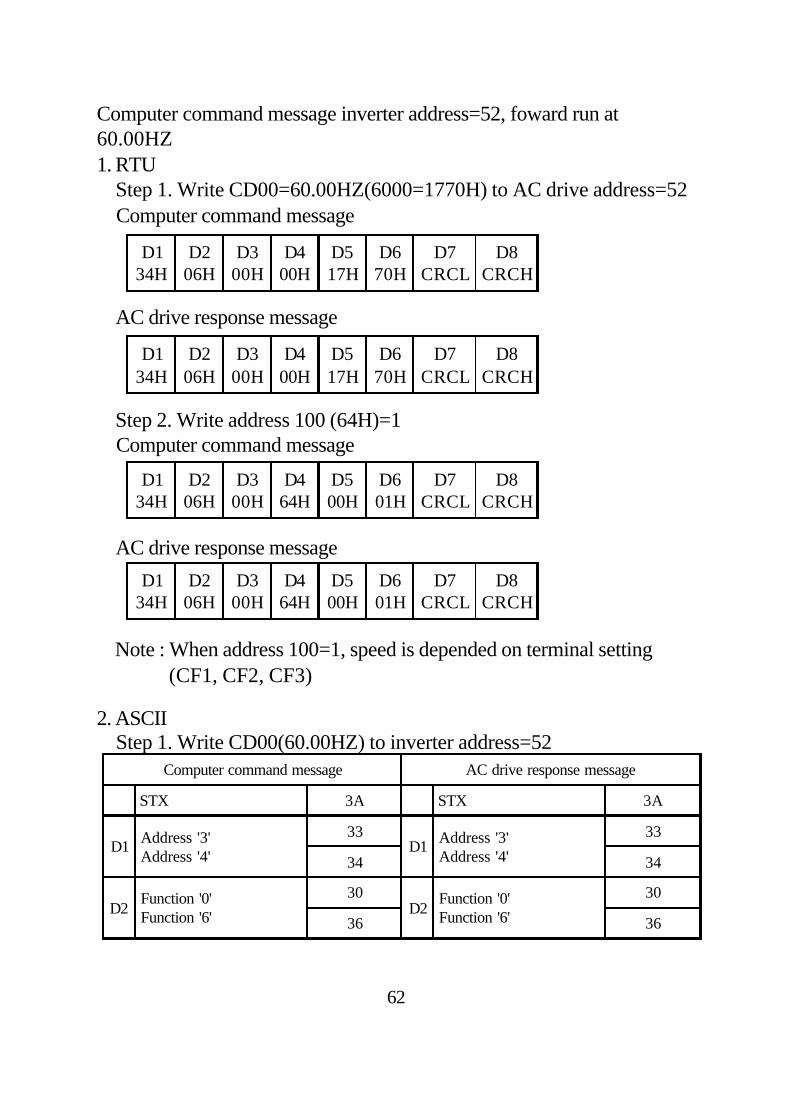
Computer command message inverter address=52, foward run at60.00HZ1. RTU Step 1. Write CD00=60.00HZ(6000=1770H) to AC drive address=52 Computer command message
AC drive response message
Step 2. Write address 100 (64H)=1 Computer command message
AC drive response message
Note : When address 100=1, speed is depended on terminal setting (CF1, CF2, CF3)
2. ASCII Step 1. Write CD00(60.00HZ) to inverter address=52
D134H
D206H
D300H
D400H
D517H
D670H
D7CRCL
D8CRCH
D134H
D206H
D300H
D400H
D517H
D670H
D7CRCL
D8CRCH
62
D134H
D206H
D300H
D464H
D500H
D601H
D7CRCL
D8CRCH
D134H
D206H
D300H
D464H
D500H
D601H
D7CRCL
D8CRCH
Computer command message AC drive response message
STX 3A STX 3A
D1 Address '3'Address '4'
33D1 Address '3'
Address '4'
33
34 34
D2Function '0'Function '6'
30D2
Function '0'Function '6'
30
36 36
63
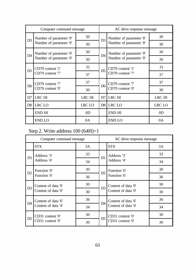
Step 2. Write address 100 (64H)=1
Computer command message AC drive response message
D3 Number of parameter '0'Number of parameter '0'
30D3 Number of parameter '0'
Number of parameter '0'
30
30 30
D4 Number of parameter '0'Number of parameter '0'
30D4 Number of parameter '0'
Number of parameter '0'
30
30 30
D5 CD79 content '1'CD79 content '7'
31D5 CD79 content '1'
CD79 content '7'
31
37 37
D6 CD79 content '7'CD79 content '0'
37D6 CD79 content '7'
CD79 content '0'
37
30 30
D7 LRC HI LRC HI D7 LRC HI LRC HI
D8 LRC LO LRC LO D8 LRC LO LRC LO
END HI 0D END HI 0D
END LO 0A END LO 0A
Computer command message AC drive response message
STX 3A STX 3A
D1 Address '3'Address '4'
33D1 Address '3'
Address '4'
33
34 34
D2Function '0'Function '6'
30D2
Function '0'Function '6'
30
36 36
D3Content of data '0'Content of data '0'
30D3
Content of data '0'Content of data '0'
30
30 30
D4Content of data '6'Content of data '4'
36D4
Content of data '6'Content of data '4'
36
34 34
D5CD31 content '0'CD31 content '0'
30D5
CD31 content '0'CD31 content '0'
30
30 30
64
AC drive response messages need to be same as command message when do communication loop detection.
Computer command message AC drive response message
D6CD31 content '0'CD31 content '1'
30D6
CD31 content '0'CD31 content '1'
30
31 31
D7 LRC HI LRC HI D7 LRC HI LRC HI
D8 LRC LO LRC LO D8 LRC LO LRC LO
END HI 0D END HI 0D
END LO 0A END LO 0A
(3) 08H : Communication loop detection
Computer command message D1 : Communication address D2 : Function code D3 : Data 1 D4 : Data 2 D5 : Data 3 D6 : Data 4 D7 : CRCL D8 : CRCH
(0~FFh)(08h)(0~FFh)(0~FFh)(0~FFh)(0~FFh)(0~FFh)(0~FFh)
AC drive response message D1 : Communication address D2 : Function code D3 : Data 1 D4 : Data 2 D5 : Data 3 D6 : Data 4 D7 : CRCL D8 : CRCH
(0~FFh)(08h)(0~FFh)(0~FFh)(0~FFh)(0~FFh)(0~FFh)(0~FFh)
65
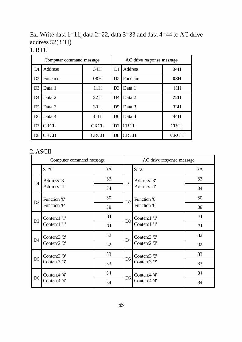
Ex. Write data 1=11, data 2=22, data 3=33 and data 4=44 to AC driveaddress 52(34H)1. RTU
2. ASCII
Computer command message AC drive response message
D1 Address 34H D1 Address 34H
D2 Function 08H D2 Function 08H
D3 Data 1 11H D3 Data 1 11H
D4 Data 2 22H D4 Data 2 22H
D5 Data 3 33H D5 Data 3 33H
D6 Data 4 44H D6 Data 4 44H
D7 CRCL CRCL D7 CRCL CRCL
D8 CRCH CRCH D8 CRCH CRCH
Computer command message AC drive response message
STX 3A STX 3A
D1 Address '3'Address '4'
33D1 Address '3'
Address '4'
33
34 34
D2Function '0'Function '8'
30D2
Function '0'Function '8'
30
38 38
D3Content1 '1'Content1 '1'
31D3
Content1 '1'Content1 '1'
31
31 31
D4Content2 '2'Content2 '2'
32D4
Content2 '2'Content2 '2'
32
32 32
D5Content3 '3'Content3 '3'
33D5
Content3 '3'Content3 '3'
33
33 33
D6Content4 '4'Content4 '4'
34D6
Content4 '4'Content4 '4'
34
34 34
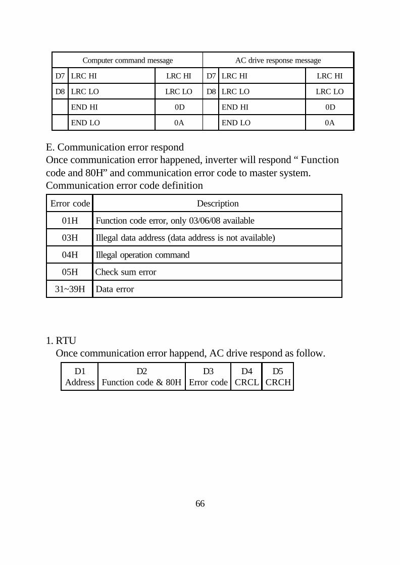
66
Computer command message AC drive response message
D7 LRC HI LRC HI D7 LRC HI LRC HI
D8 LRC LO LRC LO D8 LRC LO LRC LO
END HI 0D END HI 0D
END LO 0A END LO 0A
E. Communication error respondOnce communication error happened, inverter will respond “ Functioncode and 80H” and communication error code to master system.Communication error code definition
1. RTU Once communication error happend, AC drive respond as follow.
D1Address
D2Function code & 80H
D3Error code
D4CRCL
D5CRCH
Error code Description
01H Function code error, only 03/06/08 available
03H Illegal data address (data address is not available)
04H Illegal operation command
05H Check sum error
31~39H Data error
2. ASCII
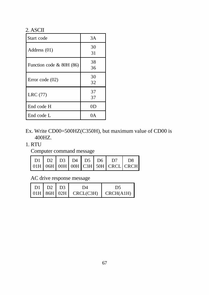
Ex. Write CD00=500HZ(C350H), but maximum value of CD00 is 400HZ.1. RTU Computer command message
AC drive response message
D101H
D206H
D300H
D400H
D5C3H
D650H
D7CRCL
D8CRCH
D101H
D286H
D302H
D4CRCL(C3H)
D5CRCH(A1H)
67
Start code 3A
Address (01) 3031
Function code & 80H (86) 3836
Error code (02) 3032
LRC (77) 3737
End code H 0D
End code L 0A
2. ASCII
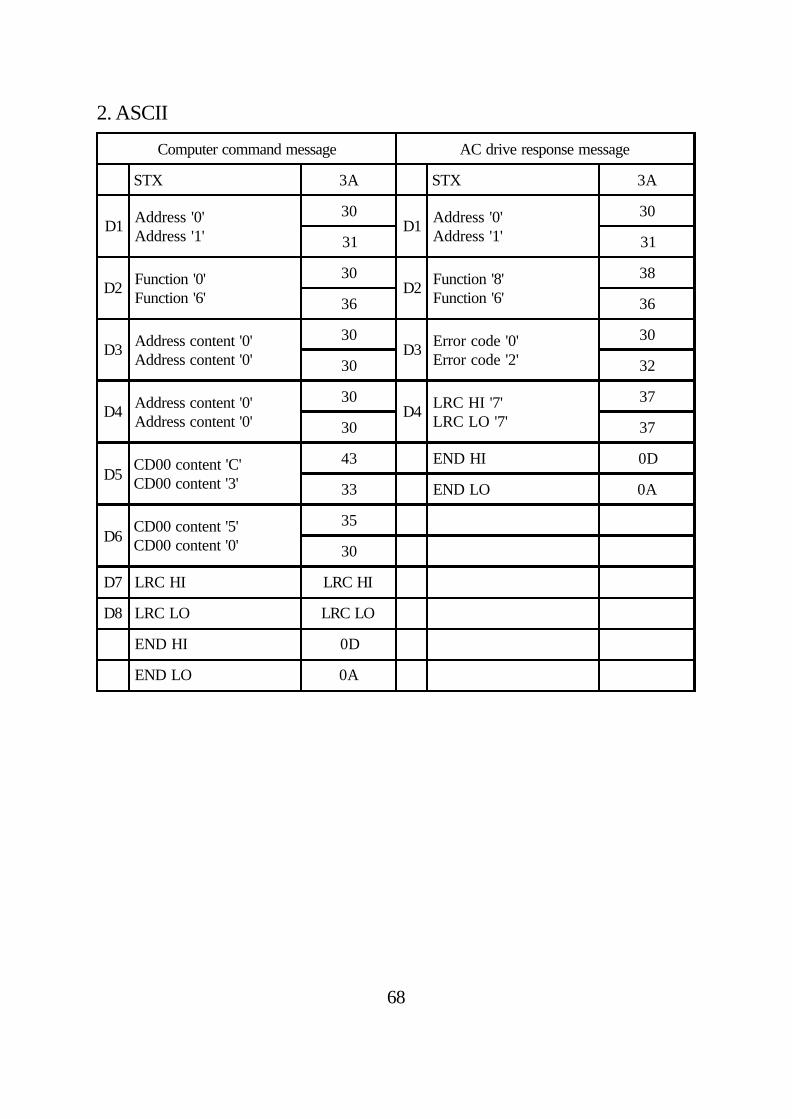
68
Computer command message AC drive response message
STX 3A STX 3A
D1 Address '0'Address '1'
30D1 Address '0'
Address '1'
30
31 31
D2 Function '0'Function '6'
30D2 Function '8'
Function '6'
38
36 36
D3 Address content '0'Address content '0'
30D3 Error code '0'
Error code '2'
30
30 32
D4 Address content '0'Address content '0'
30D4 LRC HI '7'
LRC LO '7'
37
30 37
D5CD00 content 'C'CD00 content '3'
43 END HI 0D
33 END LO 0A
D6CD00 content '5'CD00 content '0'
35
30
D7 LRC HI LRC HI
D8 LRC LO LRC LO
END HI 0D
END LO 0A
69
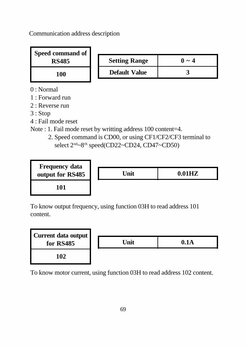
Communication address description
0 : Normal1 : Forward run2 : Reverse run3 : Stop4 : Fail mode resetNote : 1. Fail mode reset by writting address 100 content=4. 2. Speed command is CD00, or using CF1/CF2/CF3 terminal to select 2nd~8th speed(CD22~CD24, CD47~CD50)
To know output frequency, using function 03H to read address 101content.
To know motor current, using function 03H to read address 102 content.
Setting Range 0 ~ 4
Default Value 3
Speed command ofRS485
100
Frequency dataoutput for RS485
101
Unit 0.01HZ
Current data outputfor RS485
102
Unit 0.1A
70
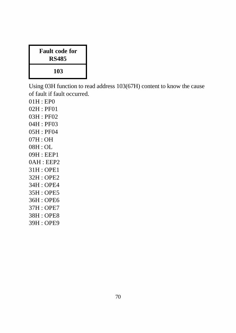
Using 03H function to read address 103(67H) content to know the causeof fault if fault occurred.01H : EP002H : PF0103H : PF0204H : PF0305H : PF0407H : OH08H : OL09H : EEP10AH : EEP231H : OPE132H : OPE234H : OPE435H : OPE536H : OPE637H : OPE738H : OPE839H : OPE9
Fault code forRS485
103
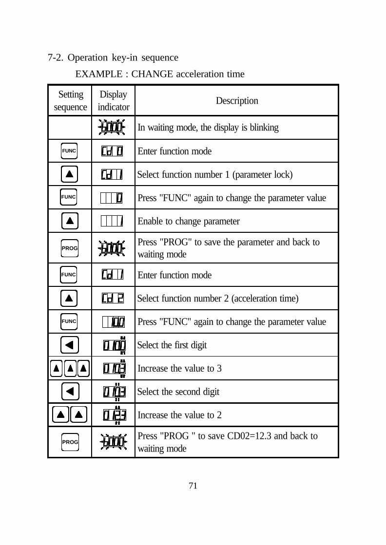
7-2. Operation key-in sequence
EXAMPLE : CHANGE acceleration time
71
Settingsequence
Displayindicator
Description
In waiting mode, the display is blinking
Enter function mode
Select function number 1 (parameter lock)
Press "FUNC" again to change the parameter value
Enable to change parameter
Press "PROG" to save the parameter and back towaiting mode
Enter function mode
Select function number 2 (acceleration time)
Press "FUNC" again to change the parameter value
Select the first digit
Increase the value to 3
Select the second digit
Increase the value to 2
Press "PROG " to save CD02=12.3 and back towaiting mode
FUNC
PROG
FUNC
FUNC
FUNC
PROG
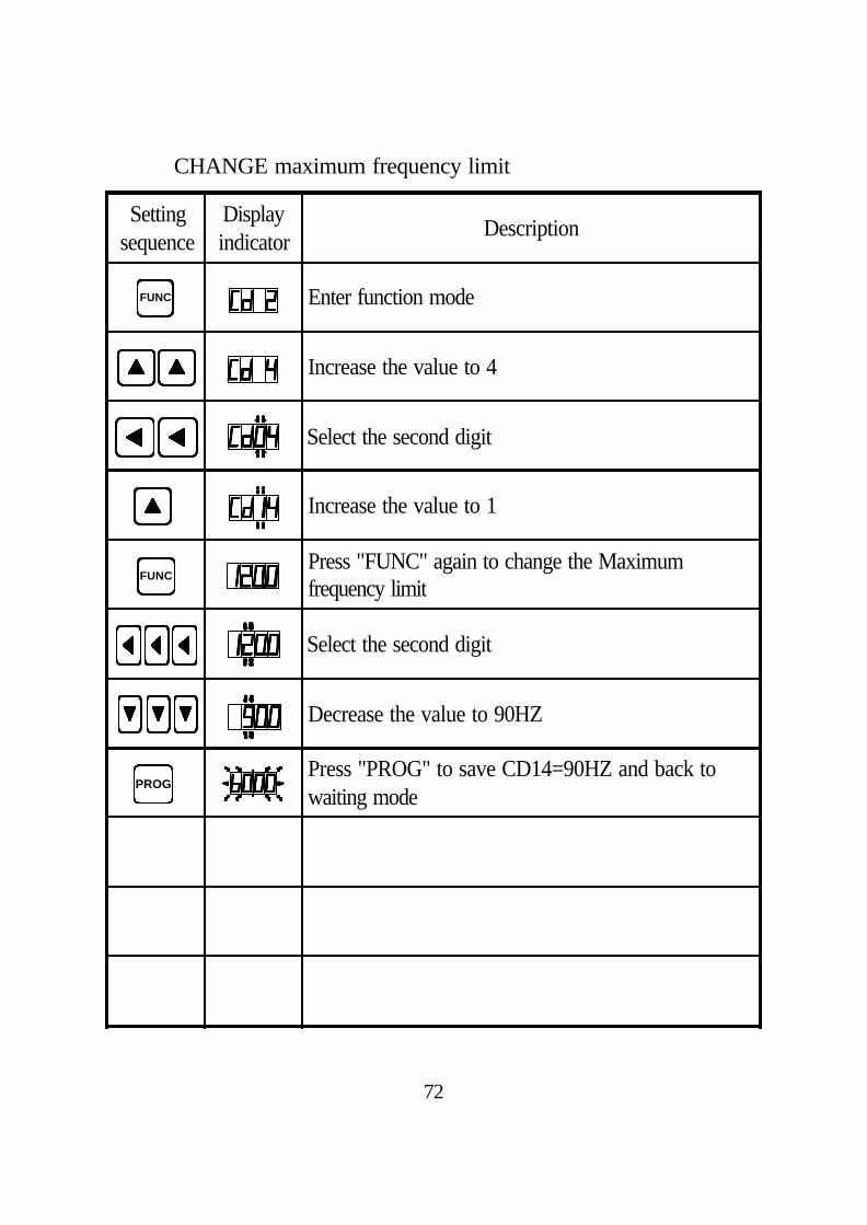
CHANGE maximum frequency limit
72
FUNC
PROG
FUNC
Settingsequence
Displayindicator Description
Enter function mode
Increase the value to 4
Select the second digit
Increase the value to 1
Press "FUNC" again to change the Maximumfrequency limit
Select the second digit
Decrease the value to 90HZ
Press "PROG" to save CD14=90HZ and back towaiting mode
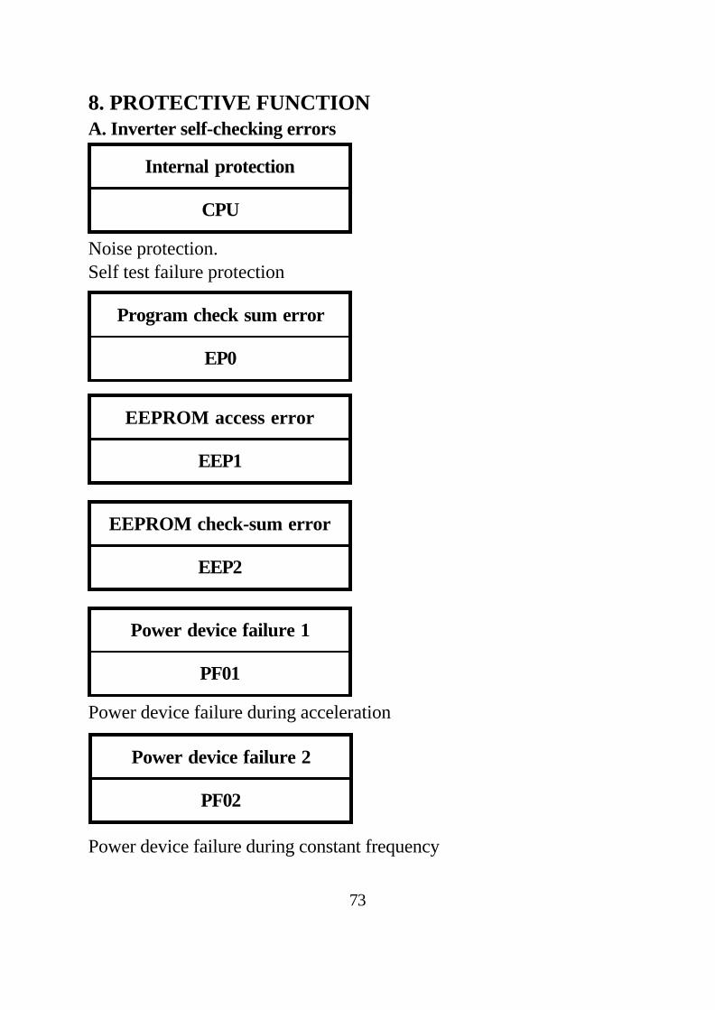
8. PROTECTIVE FUNCTIONA. Inverter self-checking errors
73
Noise protection.Self test failure protection
Power device failure during acceleration
Internal protection
CPU
Program check sum error
EP0
EEPROM access error
EEP1
EEPROM check-sum error
EEP2
Power device failure 1
PF01
Power device failure 2
PF02
Power device failure during constant frequency
Power device failure 3
PF03
Power device failure during deceleration (stopping)
Power device failure 4
PF04
Power device failure during stand-by
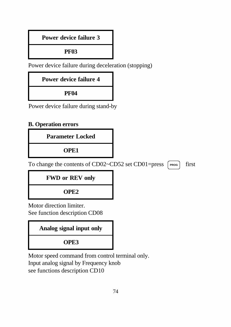
B. Operation errors
Parameter Locked
OPE1
To change the contents of CD02~CD52 set CD01=press first
FWD or REV only
OPE2
Motor direction limiter.See function description CD08
Analog signal input only
OPE3
Motor speed command from control terminal only.Input analog signal by Frequency knobsee functions description CD10
74
PROG
75
Terminal command only
OPE4
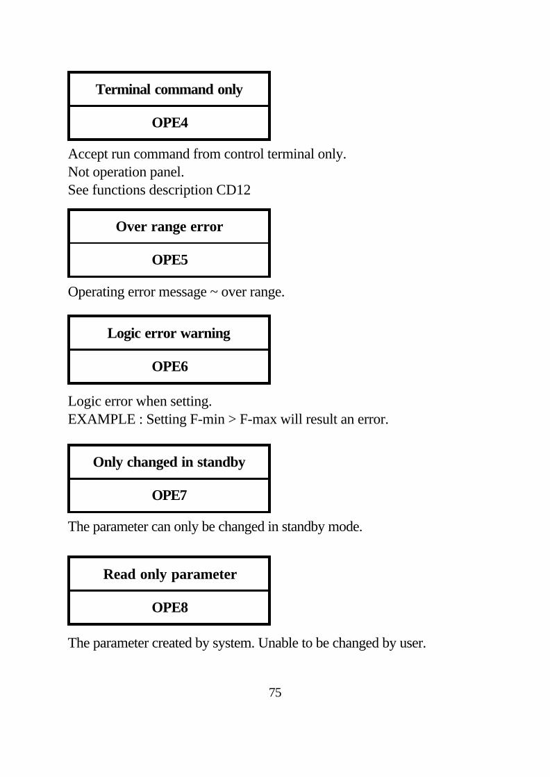
Accept run command from control terminal only.Not operation panel.See functions description CD12
Over range error
OPE5
Operating error message ~ over range.
Logic error warning
OPE6
Logic error when setting.EXAMPLE : Setting F-min > F-max will result an error.
Only changed in standby
OPE7
The parameter can only be changed in standby mode.
Read only parameter
OPE8
The parameter created by system. Unable to be changed by user.
Over heat
OH
Over temperature for external indicator. Refer to CD42 (FT1) or CD43(FT2)
76
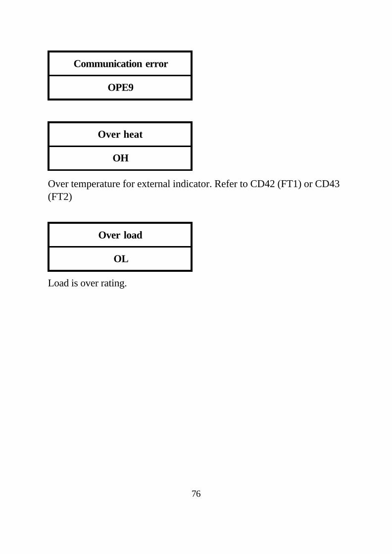
Communication error
OPE9
Over load
OL
Load is over rating.
9. PRECAUTIONS9-1 Prior to maintenance, check the following : (1) Before maintenance, be sure to turn the power off and wait until the LED digits vanish in the display. However, approx. 50 VDC still remains immediately after the display disappears, so wait a little bit longer. (2) When removing or re-installing a connector, do not pull the cable. (3) Take special care not to misplace the connector. Carefully note any disconnecting or poor contact. Be sure to tighten the terminals and connectors securely. (4) It should be noted that electronic equipment is not resistant to moisture and oil mist, and intrusion of dust or iron powder will damage the insulation, leading to an unexpencted acci- dent.
9-2 Application precautions (1) Before you start operation, thoroughly check for erroneous wiring or short circuits in the motor or in the wiring between your motor and the inverter. Do not ground the neutral point of the motor with a star connection. (2) An inverter-driven run generates a certain amount of electromagnetic noise, as compared with that of driven directly by a commercial power supply. Thus you should be aware of such limitation when using an inverter-driven motor at a noise-sensitive site. (3) Before setting the maximum frequency at 60HZ or higher, confirm that this operation range is acceptable with that of your motor. (4) When you determine an appropriate inverter capacity, ensure that the rated current of the motor does not exceed the inverter, s rated current. (5) Install a mold-case circuit breaker (MCCB) at the inverter, s power supply end to protect the wiring.
77
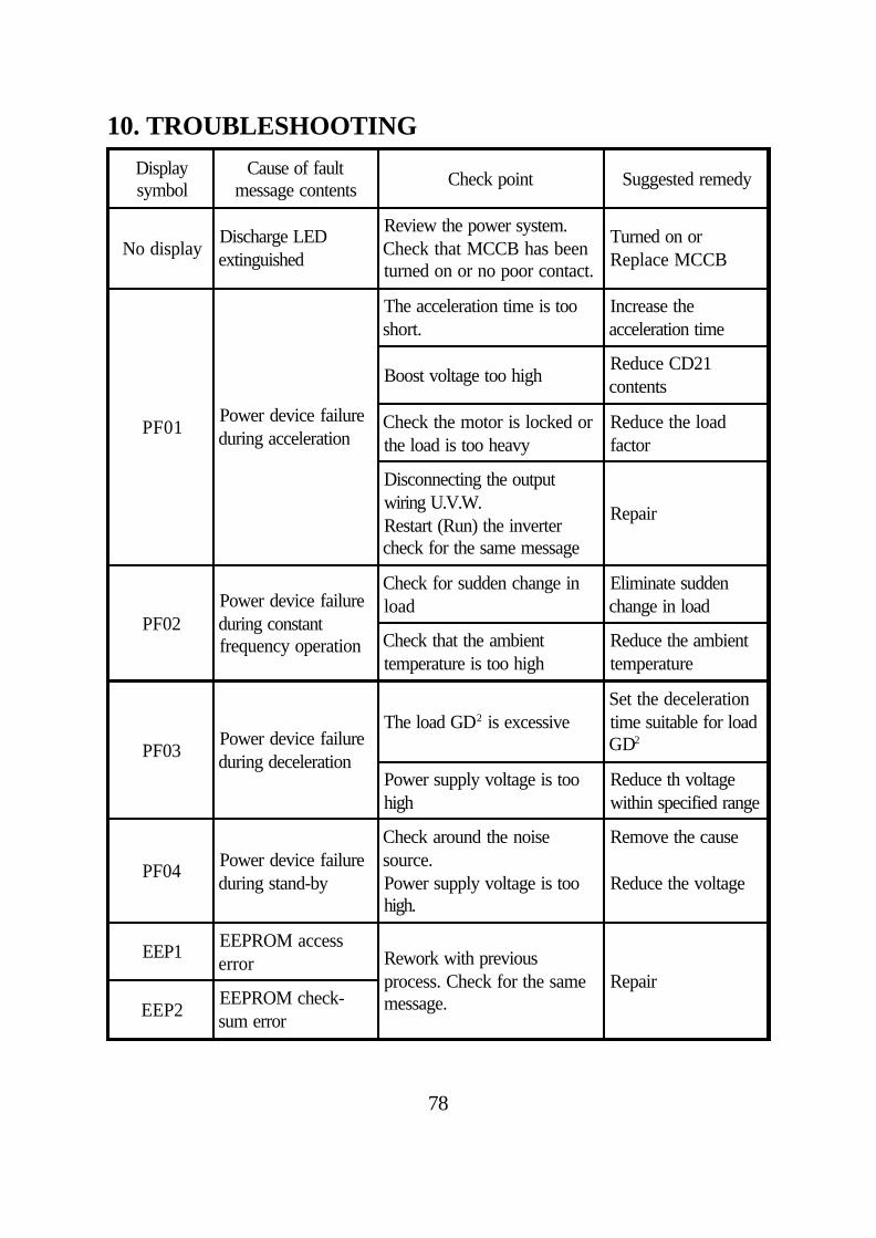
10. TROUBLESHOOTING
78
Displaysymbol
Cause of faultmessage contents Check point Suggested remedy
No displayDischarge LEDextinguished
Review the power system.Check that MCCB has beenturned on or no poor contact.
Turned on orReplace MCCB
PF01Power device failureduring acceleration
The acceleration time is tooshort.
Increase theacceleration time
Boost voltage too highReduce CD21contents
Check the motor is locked orthe load is too heavy
Reduce the loadfactor
Disconnecting the outputwiring U.V.W.Restart (Run) the invertercheck for the same message
Repair
PF02Power device failureduring constantfrequency operation
Check for sudden change inload
Eliminate suddenchange in load
Check that the ambienttemperature is too high
Reduce the ambienttemperature
PF03Power device failureduring deceleration
The load GD2 is excessiveSet the decelerationtime suitable for loadGD2
Power supply voltage is toohigh
Reduce th voltagewithin specified range
PF04 Power device failureduring stand-by
Check around the noisesource.Power supply voltage is toohigh.
Remove the cause
Reduce the voltage
EEP1 EEPROM accesserror Rework with previous
process. Check for the samemessage.
RepairEEP2
EEPROM check-sum error
11. APPLICATION
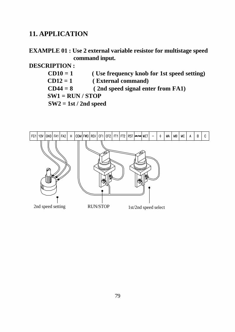
EXAMPLE 01 : Use 2 external variable resistor for multistage speed command input.DESCRIPTION : CD10 = 1 ( Use frequency knob for 1st speed setting) CD12 = 1 ( External command) CD44 = 8 ( 2nd speed signal enter from FA1) SW1 = RUN / STOP SW2 = 1st / 2nd speed
79
RUN/STOP2nd speed setting 1st/2nd speed select
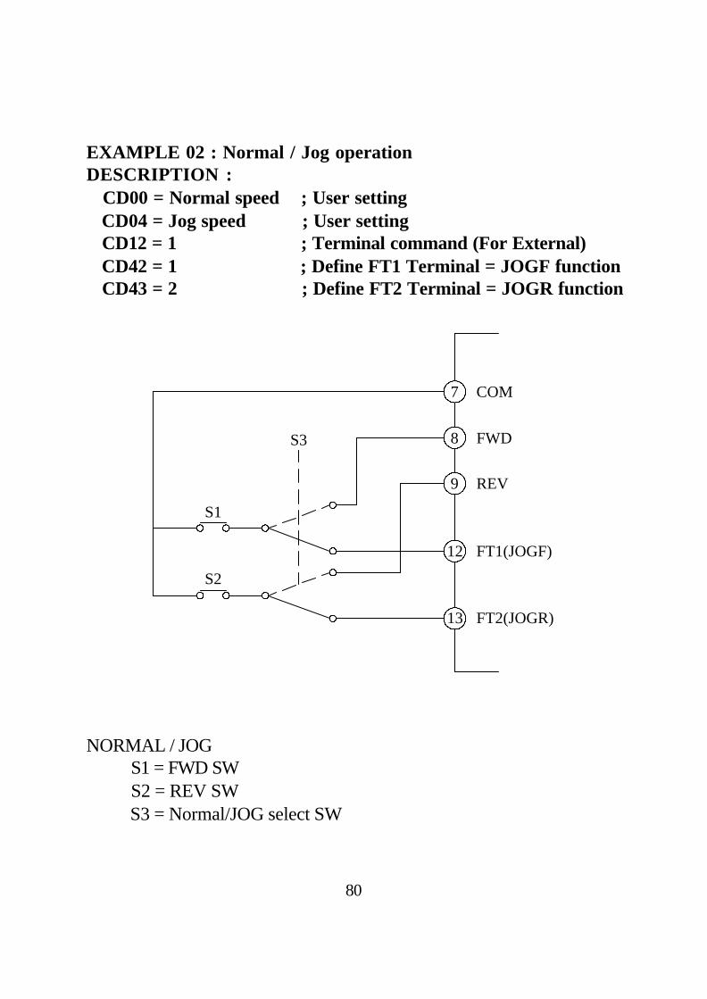
EXAMPLE 02 : Normal / Jog operationDESCRIPTION : CD00 = Normal speed ; User setting CD04 = Jog speed ; User setting CD12 = 1 ; Terminal command (For External) CD42 = 1 ; Define FT1 Terminal = JOGF function CD43 = 2 ; Define FT2 Terminal = JOGR function
NORMAL / JOG S1 = FWD SW S2 = REV SW S3 = Normal/JOG select SW
80
7
8
9
12
13
S3
S1
S2
COM
FWD
REV
FT1(JOGF)
FT2(JOGR)
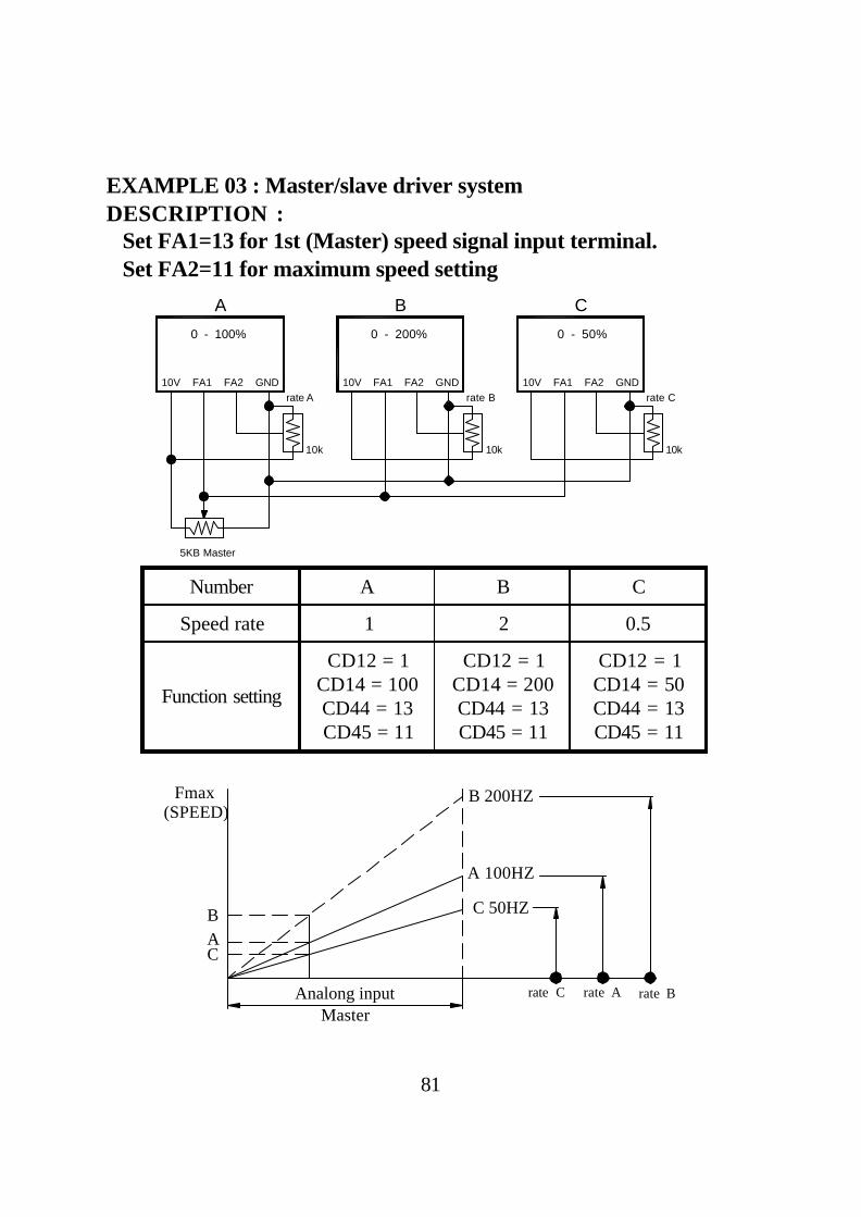
EXAMPLE 03 : Master/slave driver systemDESCRIPTION : Set FA1=13 for 1st (Master) speed signal input terminal. Set FA2=11 for maximum speed setting
81
0 - 100%
10V FA1 FA2 GND 10V FA1 FA2 GND
0 - 200%
10V FA1 FA2 GND
0 - 50%
A B C
rate A
10k 10k
rate B
10k
rate C
5KB Master
Number A B C
Speed rate 1 2 0.5
Function setting
CD12 = 1CD14 = 100CD44 = 13CD45 = 11
CD12 = 1CD14 = 200CD44 = 13CD45 = 11
CD12 = 1CD14 = 50CD44 = 13CD45 = 11
Fmax(SPEED)
BAC
Master
B 200HZ
A 100HZ
C 50HZ
Analong input rate C rate A rate B
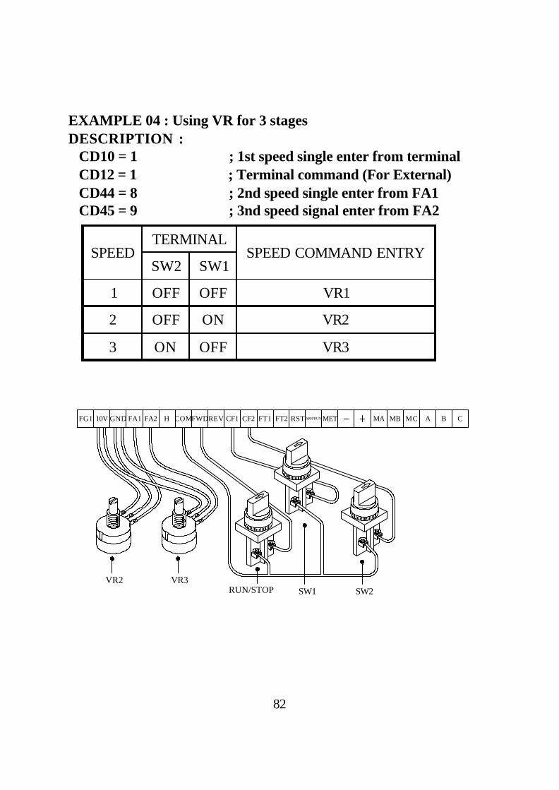
EXAMPLE 04 : Using VR for 3 stagesDESCRIPTION : CD10 = 1 ; 1st speed single enter from terminal CD12 = 1 ; Terminal command (For External) CD44 = 8 ; 2nd speed single enter from FA1 CD45 = 9 ; 3nd speed signal enter from FA2
SPEEDTERMINAL
SPEED COMMAND ENTRYSW2 SW1
1 OFF OFF VR1
2 OFF ON VR2
3 ON OFF VR3
82
RSTFA2GND10VFG1 FA1 COMH REVFWD CF2CF1 FT2FT1 METARR/RUN MBMA MC A CB
RUN/STOP SW1VR2 VR3
SW2
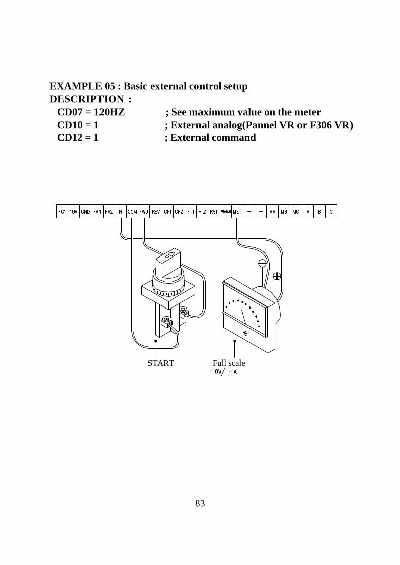
EXAMPLE 05 : Basic external control setupDESCRIPTION : CD07 = 120HZ ; See maximum value on the meter CD10 = 1 ; External analog(Pannel VR or F306 VR) CD12 = 1 ; External command
83
Full scaleSTART
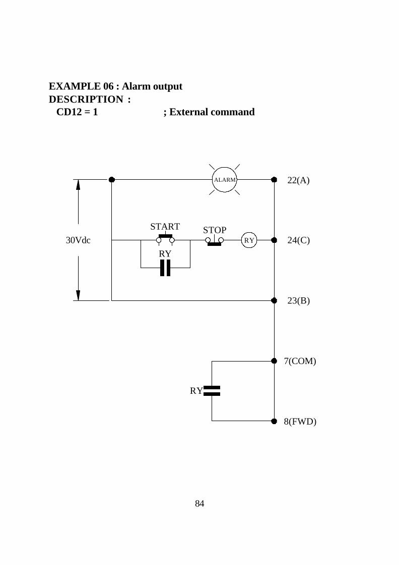
EXAMPLE 06 : Alarm outputDESCRIPTION : CD12 = 1 ; External command
84
ALARM
RYSTOPSTART
RY
RY
22(A)
24(C)
23(B)
7(COM)
8(FWD)
30Vdc
+
-
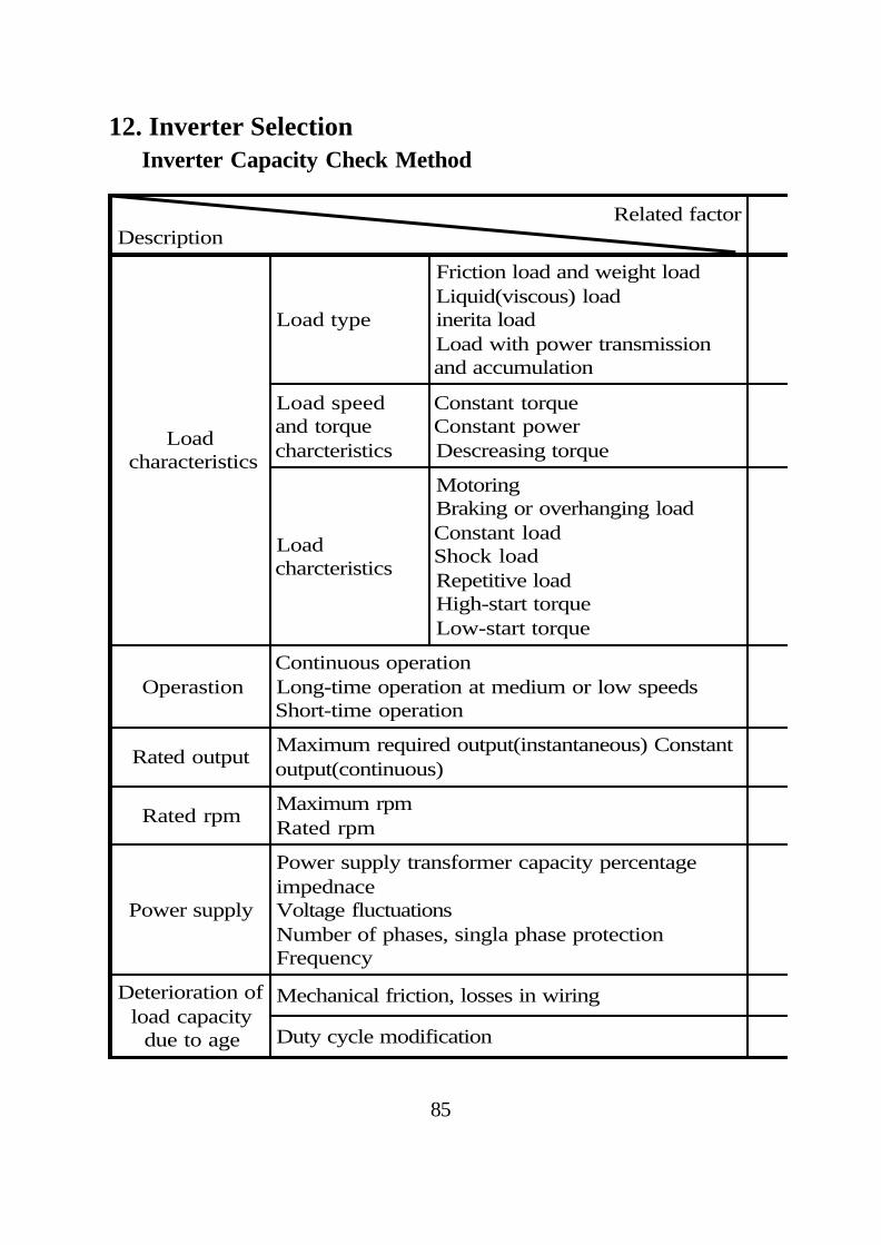
12. Inverter Selection Inverter Capacity Check Method
85
Related factorDescription
Loadcharacteristics
Load type
Friction load and weight loadLiquid(viscous) loadinerita loadLoad with power transmissionand accumulation
Load speedand torquecharcteristics
Constant torqueConstant powerDescreasing torque
Loadcharcteristics
MotoringBraking or overhanging loadConstant loadShock loadRepetitive loadHigh-start torqueLow-start torque
OperastionContinuous operationLong-time operation at medium or low speedsShort-time operation
Rated outputMaximum required output(instantaneous) Constantoutput(continuous)
Rated rpmMaximum rpmRated rpm
Power supply
Power supply transformer capacity percentageimpednaceVoltage fluctuationsNumber of phases, singla phase protectionFrequency
Deterioration ofload capacity
due to age
Mechanical friction, losses in wiring
Duty cycle modification
86
Speed andTorque
CharacteristicsTime Ratings
OverloadCapacity Starting torque
※ ※
※ ※
※ ※ ※ ※
※ ※
※ ※
※
※ ※
※ ※
※
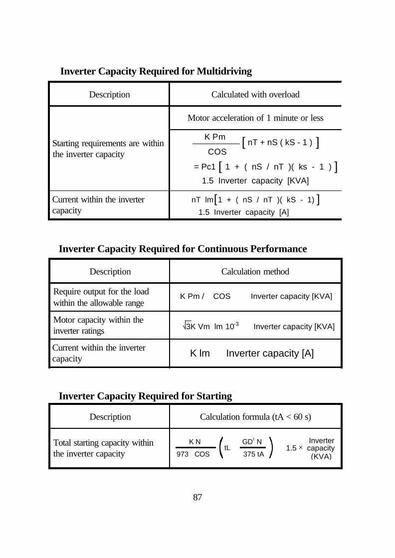
Inverter Capacity Required for Multidriving
Inverter Capacity Required for Continuous Performance
Inverter Capacity Required for Starting
K lm Inverter capacity [A] ≦
nT lm 1 + ( nS / nT )( kS - 1)
1.5 Inverter capacity [A]
[ ] ≦
1.5 capacityInverter
(KVA)≦ ×
Description Calculation method
Require output for the loadwithin the allowable range
Motor capacity within theinverter ratings
Current within the invertercapacity
87
Description Calculation formula (tA < 60 s)
Total starting capacity withinthe inverter capacity
Description Calculated with overload
Starting requirements are withinthe inverter capacity
Motor acceleration of 1 minute or less
Current within the invertercapacity
K N
973 COS∮tL+
375 tA
GD N2
η
K Pm / COS Inverter capacity [KVA]≦ η ∮
K Pm
COSnT + nS ( kS - 1 )[ ]
= Pc1 1 + ( nS / nT )( ks - 1 )
1.5 Inverter capacity [KVA]
[ ]≦
η ∮
3K Vm lm Inverter capacity [KVA]10-3≦
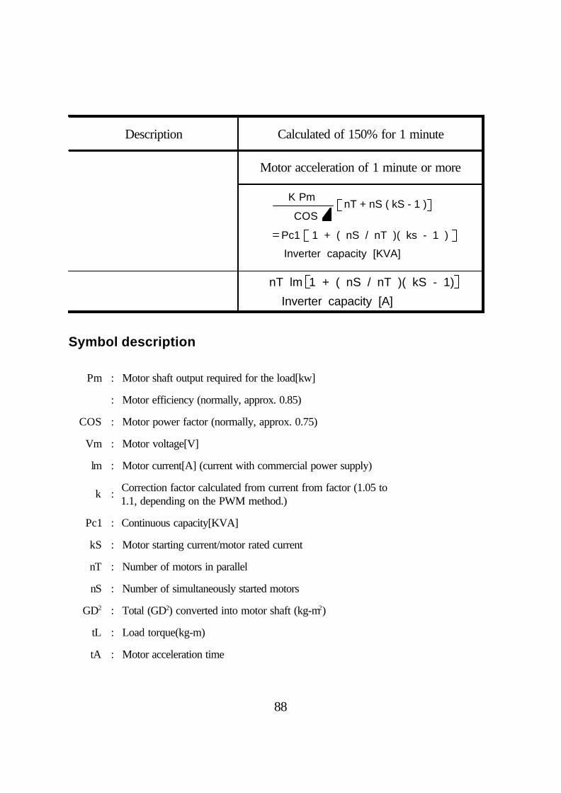
Symbol description
K Pm
COSnT + nS ( kS - 1 )
Pc1 1 + ( nS / nT )( ks - 1 )
Inverter capacity [KVA]
ψ
nT lm 1 + ( nS / nT )( kS - 1)
Inverter capacity [A]
Description Calculated of 150% for 1 minute
Motor acceleration of 1 minute or more
88
≦
≦
Pm : Motor shaft output required for the load[kw]
: Motor efficiency (normally, approx. 0.85)
COS : Motor power factor (normally, approx. 0.75)
Vm : Motor voltage[V]
lm : Motor current[A] (current with commercial power supply)
k : Correction factor calculated from current from factor (1.05 to1.1, depending on the PWM method.)
Pc1 : Continuous capacity[KVA]
kS : Motor starting current/motor rated current
nT : Number of motors in parallel
nS : Number of simultaneously started motors
GD2 : Total (GD2) converted into motor shaft (kg-m2)
tL : Load torque(kg-m)
tA : Motor acceleration time
η
η
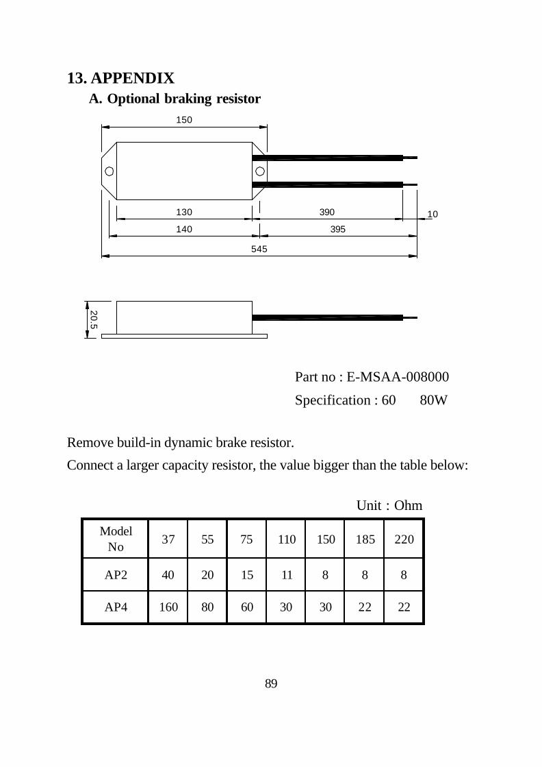
13. APPENDIX A. Optional braking resistor
Remove build-in dynamic brake resistor.
Connect a larger capacity resistor, the value bigger than the table below:
89
Unit : Ohm
Part no : E-MSAA-008000
Specification : 60 80W
ModelNo 37 55 75 110 150 185 220
AP2 40 20 15 11 8 8 8
AP4 160 80 60 30 30 22 22
Ω
150
130 390 10
545
395140
20.5
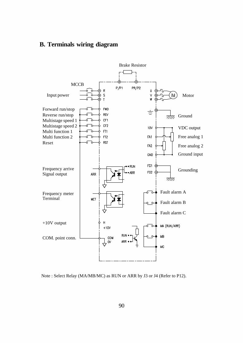
B. Terminals wiring diagram
90
Brake Resistor
COM. point conn.
+10V output
Frequency meter
Multistage speed 2Multistage speed 1
Multi function 2Multi function 1
Reverse run/stopForward run/stop
Frequency arrive
Reset
Input power
MCCB
Fault alarm C
Fault alarm B
Ground
Fault alarm A
Free analog 1
Free analog 2
Ground input
VDC output
Motor
Grounding
Note : Select Relay (MA/MB/MC) as RUN or ARR by J3 or J4 (Refer to P12).
Terminal
Signal output
C. Remote operator
UNIT : M/M
91
A-0000-F306G3 F306 Remote operator
E-092A-010200 1 meter extension cable
E-092A-030200 3 meter extension cable
E-092A-050200 5 meter extension cable

MEMO

MEMO

MEMO

MEMO

MEMO

MEMO
ADLEEPOWER SERVICE OFFICE
R
FREQUNCY INVERTER MOTOR DRIVES
JUL. 2008 2nd edition
TaiwanTel No : 886-4-25622651Fax No : 886-4-25628289E-mail : [email protected] : http://www.adlee.com
Hong KongTel No : 852-24081937Fax No : 852-24071036
Guang Dong (China)Tel No : 86-757-26656498Fax No : 86-757-26658515
Wu Han (China)Tel No : 86-27-59322991Fax No : 86-27-59322992
Shanghai (China)Tel No : 86-21-64843529Fax No : 86-21-64837594
INSTRUCTION MANUAL
PART NO : E-PHAA-EAPA03
Model : APxG3 series