Embed Size (px)
Citation preview

© 2003 Xilinx, Inc. All Rights Reserved For Academic Use Only
Introduction to Xilinx
FPGA Design Workshop

Basic FPGA Architecture 2 - 3 © 2003 Xilinx, Inc. All Rights Reserved For Academic Use Only
Objectives
Describe who Xilinx isDescribe where Programmable Logic fits into the Engineering CurriculumsList the Xilinx Products necessary to set up a lab
After completing this section, you will be able to. . .

Basic FPGA Architecture 2 - 4 © 2003 Xilinx, Inc. All Rights Reserved For Academic Use Only
Who is Xilinx?World’s leading innovator of complete programmable logic solutions
Inventor of the Field Programmable Gate ArrayFabless* Semiconductor and Software Company
UMC (Taiwan) {*Xilinx acquired an equity stake in UMC in 1996}
Seiko Epson (Japan)TSMC (Taiwan)
Programmable Logic Devices ISE Alliance and Foundation
Series Design Software

Basic FPGA Architecture 2 - 5 © 2003 Xilinx, Inc. All Rights Reserved For Academic Use Only
Electronic ComponentsSource: Dataquest Logic
StandardLogic ASIC
ProgrammableLogic Devices(PLDs)
GateArrays
Cell-BasedICs
Full CustomICs
CPLDsSPLDs(PALs) FPGAs
AcronymsSPLD = Simple Prog. Logic Device PAL = Prog. Array of LogicCPLD = Complex PLDFPGA = Field Prog. Gate Array
Common ResourcesConfigurable Logic Blocks (CLB)
– Memory Look-Up Table– AND-OR planes– Simple gates
Input / Output Blocks (IOB)– Bidirectional, latches, inverters, pullup/pulldowns
Interconnect or Routing– Local, internal feedback, and global

Basic FPGA Architecture 2 - 6 © 2003 Xilinx, Inc. All Rights Reserved For Academic Use Only
• No high development cost barriers• Recovered time for authoring and innovating
– SW improvements reduce design iterations
• No lengthy prototyping cycle• Ability to remotely upgrade any networked system• Ultimate flexibility to manage rapid change
Programmable Logic Solution

Basic FPGA Architecture 2 - 7 © 2003 Xilinx, Inc. All Rights Reserved For Academic Use Only
Where Programmable Logic Fits into the Electronics Industry
• Processor• Memory• Logic
Xilinx is the Leading Innovator of
Complete Programmable Logic Solutions
Xilinx is the Leading Innovator of
Complete Programmable Logic Solutions
Key components of an electronics system:

Basic FPGA Architecture 2 - 8 © 2003 Xilinx, Inc. All Rights Reserved For Academic Use Only
Where Programmable Logic Fits into Engineering Curriculums
Engineering LabsResearch ProjectsSenior Design ProjectsDesign Contests
Basic FPGA Architecture 2 - 9 © 2003 Xilinx, Inc. All Rights Reserved For Academic Use Only
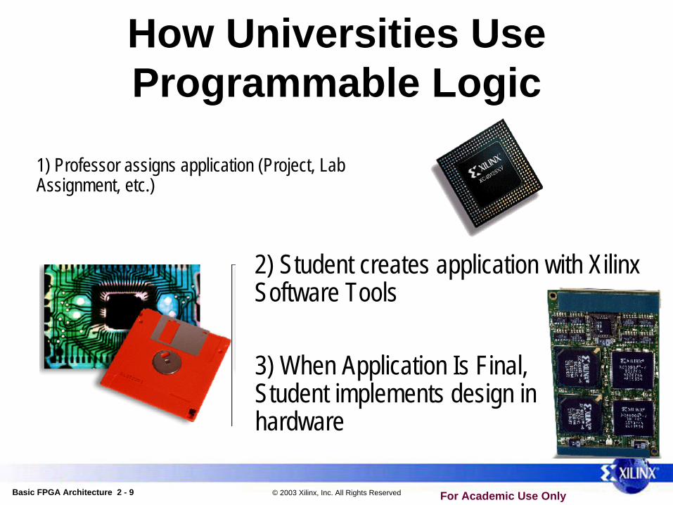
1) Professor assigns application (Project, Lab Assignment, etc.)
2) Student creates application with Xilinx Software Tools
3) When Application Is Final, Student implements design in hardware
How Universities Use Programmable Logic

Basic FPGA Architecture 2 - 10 © 2003 Xilinx, Inc. All Rights Reserved For Academic Use Only
Xilinx ProductsCPLDs and FPGAs
Architecture PAL/22V10-like Gate array-likeMore Combinational More Registers + RAM
Density Low-to-medium Medium-to-high0.5-10K logic gates 1K to 3.2M system gates
Performance Predictable timing Application dependentUp to 250 MHz today Up to 200 MHz today
Interconnect “Crossbar Switch” Incremental
Complex Programmable Logic Device (CPLD)
Field-Programmable Gate Array (FPGA)

Basic FPGA Architecture 2 - 11 © 2003 Xilinx, Inc. All Rights Reserved For Academic Use Only
Xilinx Products Design Tools
v6.2i ISE SoftwareComplete Software Package
– Design Entry (Schematic, VHDL, Verilog)– Synthesis (XST) – Implementation (Translate, Map, Place & Route)– Simulation (Modelsim)– iMPACT Programmer (Download Bistream)
CORE Generator – Parameterizable Cores
StateCAD/State Bencher– State Machine Design
HDL Bencher– Test Bench Generation
Unix, Linux, & PC Platforms

Basic FPGA Architecture 2 - 12 © 2003 Xilinx, Inc. All Rights Reserved For Academic Use Only
• New leading-edge device families
• ISE advantages can be leveraged across various Engineering courses– Across all device families and design sizes
6.2i Device Support all Xilinx leading FPGA/CPLD families

Basic FPGA Architecture 2 - 13 © 2003 Xilinx, Inc. All Rights Reserved For Academic Use Only
Programmable Logic Design Flow
XC4000XC4000XC4000
3
Design Entry & Synthesis in schematic, ABEL, VHDL, and/or Verilog.
Implementation includes Placement & Routing and bitstream generation using Xilinx’s M1 Technology. Also, analyze timing, view layout, and more.
Download directly to the Xilinx hardware device(s) with unlimited reconfigurations* !!
1
2

© 2003 Xilinx, Inc. All Rights Reserved For Academic Use Only
Basic FPGA Architecture
FPGA Design Flow Workshop

Basic FPGA Architecture 2 - 15 © 2003 Xilinx, Inc. All Rights Reserved For Academic Use Only
Objectives
After completing this module, you will be able to:• Recognize the basic architectural resources of the Virtex®-II FPGA• List the differences between Virtex-II, Virtex-II Pro™, and Spartan®-3

Basic FPGA Architecture 2 - 16 © 2003 Xilinx, Inc. All Rights Reserved For Academic Use Only
Outline
• Overview• Slice Resources• I/O Resources• Other Virtex-II Features• Spartan-3 versus Virtex-II• Virtex-II Pro Features• Summary• Appendix

Basic FPGA Architecture 2 - 17 © 2003 Xilinx, Inc. All Rights Reserved For Academic Use Only
Overview
• All Xilinx FPGAs contain the same basic resources– Slices contain combinatorial logic and register resources– IOBs interface between the FPGA and the outside world– Programmable interconnect – Other resources
• Global clock buffers• Boundary scan logic
Basic FPGA Architecture 2 - 18 © 2003 Xilinx, Inc. All Rights Reserved For Academic Use Only
Outline
• Overview• Slice Resources• I/O Resources• Other Virtex-II Features• Spartan-3 versus Virtex-II• Virtex-II Pro Features• Summary• Appendix

Basic FPGA Architecture 2 - 19 © 2003 Xilinx, Inc. All Rights Reserved For Academic Use Only
Slices and CLBs
• Each Virtex™-II CLB contains four slices
– Local routing provides feedback between slices in the same CLB, and it provides routing to neighboring CLBs
– A switch matrix provides access to general routing resources
CIN
SwitchMatrix
BUFTBUF T
COUTCOUT
Slice S0
Slice S1
Local Routing
Slice S2
Slice S3
CIN
SHIFT

Basic FPGA Architecture 2 - 20 © 2003 Xilinx, Inc. All Rights Reserved For Academic Use Only
Slice 0
LUT Carry
LUT Carry D QCE
PRE
CLR
DQCE
PRE
CLR
Simplified Slice Structure
• Each slice has four outputs– Two registered outputs,
two non-registered outputs– Two BUFTs associated
with each CLB, accessible by all 16 CLB outputs
• Carry logic runs vertically, up only
– Two independent carry chains per CLB

Basic FPGA Architecture 2 - 21 © 2003 Xilinx, Inc. All Rights Reserved For Academic Use Only
Detailed Slice Structure
• The next slides will discuss the slice features
– LUTs– MUXF5, MUXF6,
MUXF7, MUXF8 (only the F5 and F6 MUX are shown in the diagram)
– Carry Logic– MULT_ANDs– Sequential Elements

Basic FPGA Architecture 2 - 22 © 2003 Xilinx, Inc. All Rights Reserved For Academic Use Only
Combinatorial Logic
AB
CD
Z
Look-Up Tables
• Combinatorial logic is stored in Look-Up Tables (LUTs) – Also called Function Generators (FGs)– Capacity is limited by number of inputs, not complexity
• Delay through the LUT is constant
A B C D Z0 0 0 0 00 0 0 1 00 0 1 0 00 0 1 1 10 1 0 0 10 1 0 1 1
. . .1 1 0 0 01 1 0 1 01 1 1 0 01 1 1 1 1
Basic FPGA Architecture 2 - 23 © 2003 Xilinx, Inc. All Rights Reserved For Academic Use Only
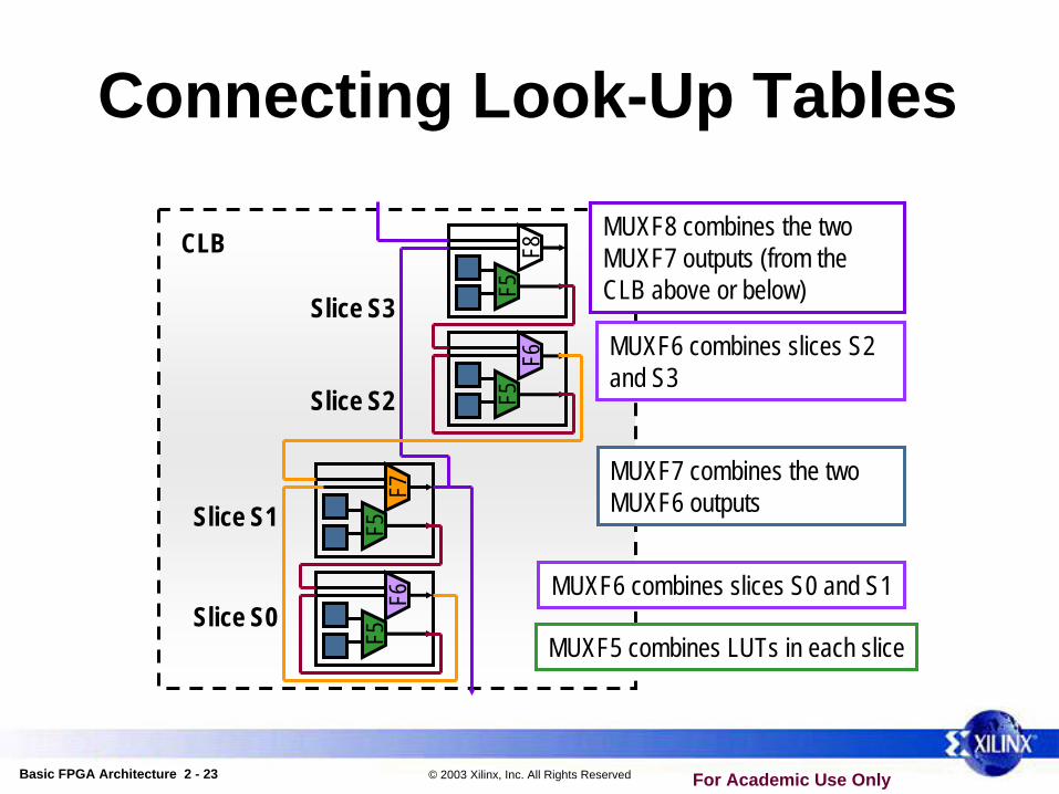
Connecting Look-Up Tables
F5F8
F5F6
CLB
Slice S3
Slice S2
Slice S0
Slice S1 F5F7
F5F6
MUXF8 combines the two MUXF7 outputs (from the CLB above or below)
MUXF6 combines slices S2 and S3
MUXF7 combines the two MUXF6 outputs
MUXF6 combines slices S0 and S1
MUXF5 combines LUTs in each slice

Basic FPGA Architecture 2 - 24 © 2003 Xilinx, Inc. All Rights Reserved For Academic Use Only
Fast Carry Logic
• Simple, fast, and complete arithmetic Logic
– Dedicated XOR gate for single- level sum completion
– Uses dedicated routing resources
– All synthesis tools can infer carry logic

Basic FPGA Architecture 2 - 25 © 2003 Xilinx, Inc. All Rights Reserved For Academic Use Only
CODI CIS
LUT
CY_MUX
CY_XOR
MULT_AND
A
B
A x B
LUT
LUT
MULT_AND Gate
• Highly efficient multiply and add implementation– Earlier FPGA architectures require two LUTs per bit to perform the
multiplication and addition– The MULT_AND gate enables an area reduction by performing the
multiply and the add in one LUT per bit

Basic FPGA Architecture 2 - 26 © 2003 Xilinx, Inc. All Rights Reserved For Academic Use Only
Flexible Sequential Elements
• Can be flip-flops or latches• Two in each slice; eight in each CLB• Inputs can come from LUTs or from an
independent CLB input• Separate set and reset controls
– Can be synchronous or asynchronous• All controls are shared within a slice
– Control signals can be inverted locally within a slice
DCE
PRE
CLR
Q
FDCPE
DCE
S
R
Q
FDRSE
DCE
PRE
CLR
Q
LDCPE
G
_1

Basic FPGA Architecture 2 - 27 © 2003 Xilinx, Inc. All Rights Reserved For Academic Use Only
LUT
Shift Register LUT (SRL16CE)
• Dynamically addressable serial shift registers
– Maximum delay of 16 clock cycles per LUT (128 per CLB)
– Cascadable to other LUTs or CLBs for longer shift registers
• Dedicated connection from Q15 to D input of the next SRL16CE
– Shift register length can be changed asynchronously by toggling address A
D QCE
D QCE
D QCE
D QCE
LUTD
CECLK
A[3:0]
Q
Q15 (cascade out)

Basic FPGA Architecture 2 - 28 © 2003 Xilinx, Inc. All Rights Reserved For Academic Use Only
Shift Register LUT Example
• The SRL can be used to create a No Operation (NOPs)– This example uses 64 LUTs (8 CLBs) to replace 576 flip-flops (72 CLBs)
and associated routing and delays
12 Cycles
64Operation A
4 Cycles 8 Cycles
Operation B
3 Cycles
Operation C
64
12 Cycles
Paths are StaticallyBalanced
9 Cycles
Operation D - NOP

Basic FPGA Architecture 2 - 29 © 2003 Xilinx, Inc. All Rights Reserved For Academic Use Only
Outline
• Overview• Slice Resources• I/O Resources• Other Virtex-II Features• Spartan-3 versus Virtex-II• Virtex-II Pro Features• Summary• Appendix

Basic FPGA Architecture 2 - 30 © 2003 Xilinx, Inc. All Rights Reserved For Academic Use Only
IOB Element
• Input path– Two DDR registers
• Output path– Two DDR registers– Two 3-state enable
DDR registers• Separate clocks and
clock enables for I and O• Set and reset signals
are shared
Reg
Reg
DDR MUX
3-state
OCK1
OCK2
Reg
Reg
DDR MUX
Output
OCK1
OCK2
PAD
Reg
Reg
Input
ICK1
ICK2
IOB

Basic FPGA Architecture 2 - 31 © 2003 Xilinx, Inc. All Rights Reserved For Academic Use Only
SelectIO Standard• Allows direct connections to external signals of varied voltages and
thresholds– Optimizes the speed/noise tradeoff– Saves having to place interface components onto your board
• Differential signaling standards– LVDS, BLVDS, ULVDS– LDT– LVPECL
• Single-ended I/O standards– LVTTL, LVCMOS (3.3V, 2.5V, 1.8V, and 1.5V)– PCI-X at 133 MHz, PCI (3.3V at 33 MHz and 66 MHz)– GTL, GTLP– and more!

Basic FPGA Architecture 2 - 32 © 2003 Xilinx, Inc. All Rights Reserved For Academic Use Only
Digital Controlled Impedance (DCI)
• DCI provides– Output drivers that match the impedance of the traces– On-chip termination for receivers and transmitters
• DCI advantages– Improves signal integrity by eliminating stub reflections– Reduces board routing complexity and component count by eliminating
external resistors– Internal feedback circuit eliminates the effects of temperature, voltage, and
process variations
Basic FPGA Architecture 2 - 33 © 2003 Xilinx, Inc. All Rights Reserved For Academic Use Only
Outline
• Overview• Slice Resources• I/O Resources• Other Virtex-II Features• Spartan-3 versus Virtex-II• Virtex-II Pro Features• Summary• Appendix

Basic FPGA Architecture 2 - 34 © 2003 Xilinx, Inc. All Rights Reserved For Academic Use Only
Other Virtex-II Features
• Distributed RAM and block RAM– Distributed RAMs use the CLB resources (1 LUT = 16 RAM bits)– Block RAMs are dedicated resources on the device (18k bit blocks)
• Dedicated 18 x 18 multipliers next to block RAMs• Clock management resources
– Sixteen dedicated global clock multiplexers– Digital Clock Managers (DCMs)

Basic FPGA Architecture 2 - 35 © 2003 Xilinx, Inc. All Rights Reserved For Academic Use Only
Distributed SelectRAM Resources
• Uses a LUT in a slice as memory• Synchronous write• Asynchronous read
– Accompanying flip-flops can be used to create synchronous read
• RAM and ROM are initialized during configuration
– Data can be written to RAM after configuration
• Emulated dual-port RAM – One read/write port– One read-only port
RAM16X1S
O
DWE
WCLKA0A1A2A3
LUT
RAM32X1S
O
DWE
WCLKA0A1A2A3A4
RAM16X1D
SPO
DWE
WCLKA0A1A2A3DPRA0 DPODPRA1DPRA2DPRA3
Slice
LUT
LUT

Basic FPGA Architecture 2 - 36 © 2003 Xilinx, Inc. All Rights Reserved For Academic Use Only
Block SelectRAM Resources
• Up to 3.5 Mb of RAM in 18-kb blocks
– Synchronous read and write• True dual-port memory
– Each port has synchronous read and write capability
– Different clocks for each port • Supports initial values• Synchronous reset on output latches• Supports parity bits
– One parity bit per eight data bits

Basic FPGA Architecture 2 - 37 © 2003 Xilinx, Inc. All Rights Reserved For Academic Use Only
Dedicated Multiplier Blocks
• 18-bit twos complement signed operation• Optimized to implement multiply and accumulate functions• Multipliers are physically located next to block SelectRAM™ memory
18 x 18Multiplier
Output (36 bits)
Data_A (18 bits)
Data_B (18 bits)
4 x 4 signed8 x 8 signed12 x 12 signed18 x 18 signed

Basic FPGA Architecture 2 - 38 © 2003 Xilinx, Inc. All Rights Reserved For Academic Use Only
Global Clock Routing Resources
• Sixteen dedicated global clock multiplexers– Eight on the top-center of the die, eight on the bottom-center– Can be driven by a clock input pad, a Digital Clock Manager (DCM),
or local routing• Global clock multiplexers provide:
– Global clock enable capability (BUFGCE)– Glitch-free switching between clock signals (BUFGMUX)– Traditional clock buffer (BUFG) function
• Up to eight clock nets can be used in each quadrant of the device

Basic FPGA Architecture 2 - 39 © 2003 Xilinx, Inc. All Rights Reserved For Academic Use Only
Digital Clock Manager (DCM)
• Up to twelve DCMs per device– Located on the top and bottom edges of the die– Driven by clock input pads
• DCMs provide:– Delay-Locked Loop (DLL)– Digital Frequency Synthesizer (DFS)– Digital Phase Shifter (DPS)
• Up to four outputs of each DCM can drive onto global clock buffers– All DCM outputs can drive general routing

Basic FPGA Architecture 2 - 40 © 2003 Xilinx, Inc. All Rights Reserved For Academic Use Only
Outline
• Overview• CLB Resources• I/O Resources• Other Virtex-II Features• Spartan-3 versus Virtex-II• Virtex-II Pro Features• Summary• Appendix

Basic FPGA Architecture 2 - 41 © 2003 Xilinx, Inc. All Rights Reserved For Academic Use Only
Spartan-3 versus Virtex-II
• Lower cost• Smaller process = lower core
voltage– .09 micron versus .15 micron– Vccint = 1.2V versus 1.5V
• Different I/O standard support– New standards: 1.2V LVCMOS,
1.8V HSTL and SSTL– Default is LVCMOS, versus
LVTTL
• More I/O pins per package• Only half of the slices support
RAM or SRL16s (SLICEM)• Fewer block RAMs and multiplier
blocks– Same size and functionality
• 8 global clock multiplexers• 2 or 4 DCM blocks• No internal 3-state buffers
– 3-state buffers are in the I/O

Basic FPGA Architecture 2 - 42 © 2003 Xilinx, Inc. All Rights Reserved For Academic Use Only
SLICEM and SLICEL
• Each Spartan™-3 CLB contains four slices
– Similar to Virtex™-II• Slices are grouped in pairs
– Left-hand SLICEM (Memory)• LUTs can be configured as
memory or SRL16– Right-hand SLICEL (Logic)
• LUT can be used as logic only
CIN
SwitchMatrix
COUTCOUT
Slice X0Y0
Slice X0Y1
Fast Connects
Slice X1Y0
Slice X1Y1
CIN
SHIFTIN
Left-Hand SLICEM Right-Hand SLICEL
SHIFTOUT

Basic FPGA Architecture 2 - 43 © 2003 Xilinx, Inc. All Rights Reserved For Academic Use Only
Outline
• Overview• CLB Resources• I/O Resources• Other Virtex-II Features• Spartan-3 versus Virtex-II• Virtex-II Pro Features• Summary• Appendix

Basic FPGA Architecture 2 - 44 © 2003 Xilinx, Inc. All Rights Reserved For Academic Use Only
Virtex-II Pro Features
• 0.13 micron process• Up to 24 RocketIO™ Multi-Gigabit Transceiver (MGT) blocks
– Serializer and deserializer (SERDES)– Fibre Channel, Gigabit Ethernet, XAUI, Infiniband compliant
transceivers,…and others– 8-, 16-, and 32-bit selectable FPGA interface– 8B/10B encoder and decoder
• Up to four PowerPC RISC processor blocks– Thirty-two 32-bit General Purpose Registers (GPRs)– Low power consumption: 0.9mW/MHz– IBM CoreConnect™ bus architecture support

Basic FPGA Architecture 2 - 45 © 2003 Xilinx, Inc. All Rights Reserved For Academic Use Only
Outline
• Overview• CLB Resources• I/O Resources• Other Virtex-II Features• Spartan-3 versus Virtex-II• Virtex-II Pro Features• Summary• Appendix

Basic FPGA Architecture 2 - 46 © 2003 Xilinx, Inc. All Rights Reserved For Academic Use Only
Skills CheckSkills Check

Basic FPGA Architecture 2 - 47 © 2003 Xilinx, Inc. All Rights Reserved For Academic Use Only
Review Questions
• List the primary slice features
• List the three ways a LUT can be configured

Basic FPGA Architecture 2 - 48 © 2003 Xilinx, Inc. All Rights Reserved For Academic Use Only
Answers
• List the primary slice features– Look-up tables and function generators (two per slice, eight per CLB)– Registers (two per slice, eight per CLB)– Dedicated multiplexers (MUXF5, MUXF6, MUXF7, MUXF8)– Carry logic– MULT_AND gate
• List the three ways a LUT can be configured– Combinatorial logic– Shift register (SRL16CE)– Distributed memory

Basic FPGA Architecture 2 - 49 © 2003 Xilinx, Inc. All Rights Reserved For Academic Use Only
Summary
• Slices contain LUTs, registers, and carry logic– LUTs are connected with dedicated multiplexers and carry logic– LUTs can be configured as shift registers or memory
• IOBs contain DDR registers• SelectIO™ standards and DCI enable direct connection to multiple I/O
standards while reducing component count• Virtex™-II memory resources include:
– Distributed SelectRAM™ resources and distributed SelectROM (uses CLB LUTs)
– 18-kb block SelectRAM resources

Basic FPGA Architecture 2 - 50 © 2003 Xilinx, Inc. All Rights Reserved For Academic Use Only
Summary
• Virtex™-II contains dedicated 18 x 18 multipliers next to each block SelectRAM™ resource
• Digital Clock Managers provide:– Delay-Locked Loop (DLL)– Digital Frequency Synthesizer (DFS)– Digital Phase Shifter (DPS)

Basic FPGA Architecture 2 - 51 © 2003 Xilinx, Inc. All Rights Reserved For Academic Use Only
Where Can I Learn More?
• User Guides– http://support.xilinx.com Documentation
• Application Notes– http://support.xilinx.com Documentation App Notes
Basic FPGA Architecture 2 - 52 © 2003 Xilinx, Inc. All Rights Reserved For Academic Use Only
Outline
• Overview• CLB Resources• I/O Resources• Other Virtex-II Features• Spartan-3 versus Virtex-II• Virtex-II Pro Features• Summary• Appendix

Basic FPGA Architecture 2 - 53 © 2003 Xilinx, Inc. All Rights Reserved For Academic Use Only
Virtex-II Architecture
• Virtex™-II architecture’s core voltage operates at 1.5V
I/O Blocks (IOBs)
ConfigurableLogic Blocks (CLBs)
Clock Management (DCMs, BUFGMUXes)
Block SelectRAM™resource
Dedicated multipliers
Programmable interconnect

Basic FPGA Architecture 2 - 54 © 2003 Xilinx, Inc. All Rights Reserved For Academic Use Only
Double Data Rate Registers
• DDR registers can be clocked by– Clock and NOT(Clock) if the duty cycle is 50/50– The outputs CLK0 and CLK180 of a DCM
• If D1 = “1” and D2 = “0”, the output is a copy of Clock– Use this technique to generate a clock output that is synchronized to DDR
output data
Reg
Reg
DDR mux
FDDR
OCK1
OCK2
D1
D2PAD
OBUFClock

Basic FPGA Architecture 2 - 55 © 2003 Xilinx, Inc. All Rights Reserved For Academic Use Only
Configuration Depth Data Bits Parity Bits16k x 1 16 kb 1 08k x 2 8 kb 2 04k x 4 4 kb 4 02k x 9 2 kb 8 1
1k x 18 1 kb 16 2512 x 36 512 32 4
Dual-Port Block RAM Configurations
• Configurations available on each port
• Independent configurations on ports A and B
– Supports data width conversion, including parity bits
Port A: 8-bIN 8-bit
OUT 32-bitPort B: 32-b

Basic FPGA Architecture 2 - 56 © 2003 Xilinx, Inc. All Rights Reserved For Academic Use Only
Clock Buffer Configurations
• Clock Buffer (BUFG)– Low-skew clock distribution
• Clock Enable Buffer (BUFGCE)– Holds the clock output low when CE is
inactive– CE can be active-High or active-Low– Changes in CE are only recognized when
the clock input is low to avoid glitches and short clock pulses
OI
CE
BUFGCE
OIBUFG

Basic FPGA Architecture 2 - 57 © 2003 Xilinx, Inc. All Rights Reserved For Academic Use Only
Clock Buffer Configurations
• Clock Multiplexer (BUFGMUX)– Switches glitch-free from one
clock to another– After a change on S, the
BUFGMUX waits for the currently selected clock input to go Low
– The output is held Low until the newly selected clock goes Low, then switches
BUFG
MUX
OI1
I0
S
I0
I1
S
O
Wait for low
Switch

© 2003 Xilinx, Inc. All Rights Reserved For Academic Use Only
Xilinx Design FlowFPGA Design Flow Workshop

Basic FPGA Architecture 2 - 59 © 2003 Xilinx, Inc. All Rights Reserved For Academic Use Only
Objectives
After completing this module, you will be able to:• List the steps of the Xilinx design process• Implement an FPGA design by using default software options

Basic FPGA Architecture 2 - 60 © 2003 Xilinx, Inc. All Rights Reserved For Academic Use Only
Outline
• Overview• ISE• Summary

Basic FPGA Architecture 2 - 61 © 2003 Xilinx, Inc. All Rights Reserved For Academic Use Only
Translate
Map
Place & Route
Xilinx Design Flow
Plan & Budget HDL RTLSimulation
Synthesizeto create netlist
FunctionalSimulation
Create Bit File
Attain Timing Closure
TimingSimulation
Implement
Create Code/Schematic

Basic FPGA Architecture 2 - 62 © 2003 Xilinx, Inc. All Rights Reserved For Academic Use Only
Design Entry• Plan and budget• Two design-entry methods: HDL or schematic
– Architecture Wizard, CORE Generator™ system, and StateCAD are available to assist in design entry
• Whichever method you use, you will need a tool to generate an EDIF or NGC netlist to bring into the Xilinx implementation tools
– Popular synthesis tools: Synplify, Precision, FPGA Compiler II, and XST• Simulate the design to ensure that it works as expected!
Plan & Budget Create Code/Schematic
HDL RTLSimulation
Synthesizeto create netlist
FunctionalSimulation
. . .

Basic FPGA Architecture 2 - 63 © 2003 Xilinx, Inc. All Rights Reserved For Academic Use Only
Xilinx Implementation
• Once you generate a netlist, you can implement the design
• There are several outputs of implementation
– Reports– Timing simulation netlists– Floorplan files– FPGA Editor files– and more!
Translate
Map
Place & Route
Implement. . .
. . .

Basic FPGA Architecture 2 - 64 © 2003 Xilinx, Inc. All Rights Reserved For Academic Use Only
What is Implementation?
• More than just “Place & Route”• Implementation includes many phases
– Translate: Merge multiple design files into a single netlist– Map: Group logical symbols from the netlist (gates) into physical
components (slices and IOBs)– Place & Route: Place components onto the chip, connect them, and extract
timing data into reports• Each phase generates files that allow you to use other Xilinx tools
– Floorplanner, FPGA Editor, XPower

Basic FPGA Architecture 2 - 65 © 2003 Xilinx, Inc. All Rights Reserved For Academic Use Only
Timing Closure
• The Timing Closure Flow is a recommended method for helping designs meet their timing objectives
• Details on each part of the flow are discussed in this course and in the Designing for Performance course

Basic FPGA Architecture 2 - 66 © 2003 Xilinx, Inc. All Rights Reserved For Academic Use Only
Download
• Once a design is implemented, you must create a file that the FPGA can understand
– This file is called a bitstream: a BIT file (.bit extension)
• The BIT file can be downloaded directly to the FPGA, or it can be converted into a PROM file, which stores the programming information

Basic FPGA Architecture 2 - 67 © 2003 Xilinx, Inc. All Rights Reserved For Academic Use Only
Outline
• Overview• ISE• Summary

Basic FPGA Architecture 2 - 68 © 2003 Xilinx, Inc. All Rights Reserved For Academic Use Only
What is ISE?
• Graphical interface to design entry and implementation tools
– Access to synthesis and schematic tools
• Including third-party synthesis tools
– Implement your design with a simple double-click
• Fine-tune with easy-to-access software options

Basic FPGA Architecture 2 - 69 © 2003 Xilinx, Inc. All Rights Reserved For Academic Use Only
WebUpdate
• Automatically checks for Service Packs on the web• Alerts you when an update is available• Supports PC platform only

Basic FPGA Architecture 2 - 70 © 2003 Xilinx, Inc. All Rights Reserved For Academic Use Only
Creating a Project
• Select File New Project
• New Project Wizard guides you through the process
– Project name and location
– Target device– Software flow– Create or add
source files

Basic FPGA Architecture 2 - 71 © 2003 Xilinx, Inc. All Rights Reserved For Academic Use Only
Creating and Adding Source Files
• To include an existing source file, double-click Add Existing Source
• To create a new source file, double-click Create New Source and choose the type of file
– HDL file– IP– Schematic– State diagram– Testbench– Constraints file
Basic FPGA Architecture 2 - 72 © 2003 Xilinx, Inc. All Rights Reserved For Academic Use Only
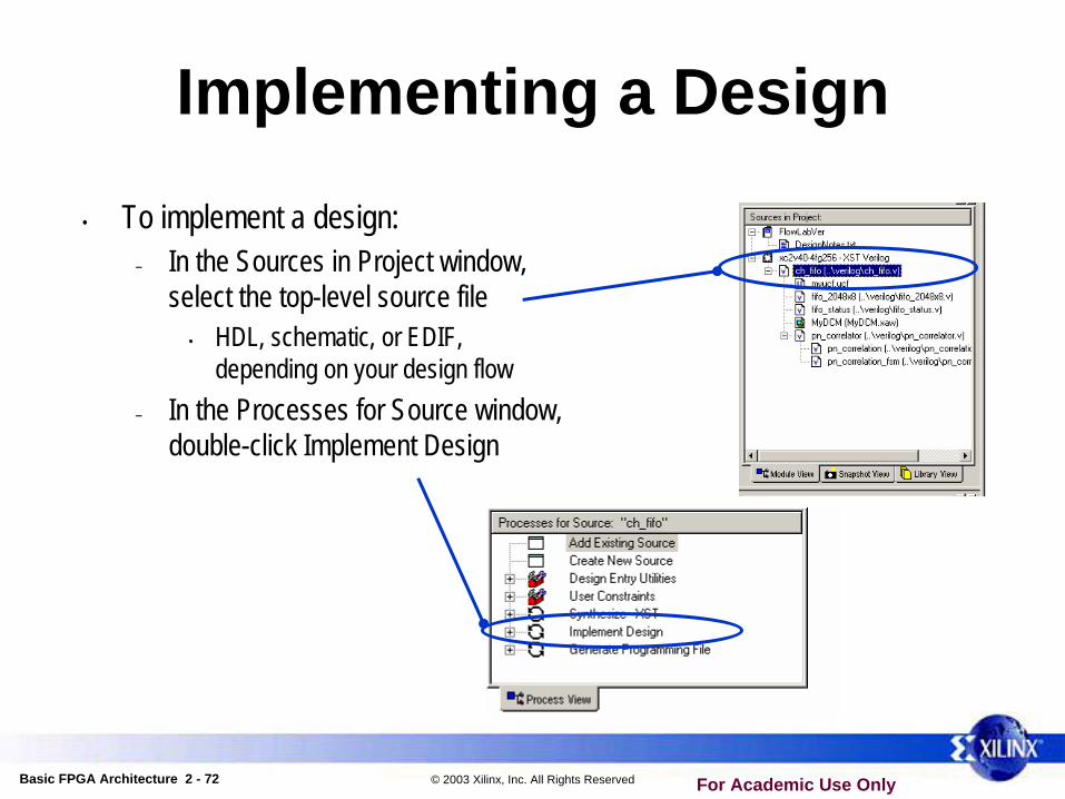
Implementing a Design
• To implement a design:– In the Sources in Project window,
select the top-level source file • HDL, schematic, or EDIF,
depending on your design flow– In the Processes for Source window,
double-click Implement Design

Basic FPGA Architecture 2 - 73 © 2003 Xilinx, Inc. All Rights Reserved For Academic Use Only
Implementation Status• ISE will run all of the necessary steps
to implement the design– Synthesize HDL code– Translate– Map– Place & Route
• Progress and status are indicated by icons– Green check mark ( ) indicates that the
process was completed successfully– Yellow exclamation point ( ! ) indicates
warnings– Yellow question mark ( ? ) indicates a file
that is out of date– Red “X” indicates errors

Basic FPGA Architecture 2 - 74 © 2003 Xilinx, Inc. All Rights Reserved For Academic Use Only
Simulating a Design
• To simulate a design:– In the Sources in Project window,
select a testbench file – In the Processes for Source window,
expand ModelSim Simulator – Double-click Simulate
Behavioral Model or Simulate Post-Place & Route Model
• Can also simulate after Translate or after Map

Basic FPGA Architecture 2 - 75 © 2003 Xilinx, Inc. All Rights Reserved For Academic Use Only
Sub-Processes
• Each process can be expanded to view sub-tools and sub-processes
– Translate• Floorplan• Assign Package Pins
– Map• Analyze timing
– Place & Route• Analyze timing• Floorplan • FPGA Editor• Analyze power• Create simulation model

Basic FPGA Architecture 2 - 76 © 2003 Xilinx, Inc. All Rights Reserved For Academic Use Only
Hierarchical Simulation Netlists
• Create separate simulation netlists and SDF files for each level of design hierarchy
– Simplifies timing verification– Allows you to re-use testbenches from behavioral simulation
• Hierarchy must be maintained during synthesis• Use the KEEP_HIERARCHY attribute in UCF file• For more information, see Answer #17693

Basic FPGA Architecture 2 - 77 © 2003 Xilinx, Inc. All Rights Reserved For Academic Use Only
Program the FPGA
• There are two ways to program an FPGA
– Through a PROM device• You will need to generate
a file that the PROM programmer will understand
– Directly from the computer• Use the iMPACT
configuration tool

Basic FPGA Architecture 2 - 78 © 2003 Xilinx, Inc. All Rights Reserved For Academic Use Only
Outline
• Overview• ISE• Summary

Basic FPGA Architecture 2 - 79 © 2003 Xilinx, Inc. All Rights Reserved For Academic Use Only
Review Questions
• What are the phases of the Xilinx design flow?
• What are the components of implementation, and what happens at each step?
• What are two methods used to program an FPGA?

Basic FPGA Architecture 2 - 80 © 2003 Xilinx, Inc. All Rights Reserved For Academic Use Only
Answers• What are the phases of the Xilinx design flow?
– Planning and budgeting, create code or schematic, RTL simulation, synthesize, functional simulation, implement, timing closure, timing simulation, BIT file creation
• What are the components of implementation, and what happens at each step?
– Translate: merges multiple design files into one netlist– Map: groups logical symbols into physical components– Place & Route: places components onto the chip and connects them together
• What are two methods used to program an FPGA?– PROM– Xilinx iMPACT configuration tool

Basic FPGA Architecture 2 - 81 © 2003 Xilinx, Inc. All Rights Reserved For Academic Use Only
Summary
• Implementation means more than place & route
• Xilinx provides a simple “pushbutton” tool to help you through the Xilinx design process

Basic FPGA Architecture 2 - 82 © 2003 Xilinx, Inc. All Rights Reserved For Academic Use Only
Where Can I Learn More?
• Complete design flow tutorials– http://support.xilinx.com Documentation Tutorials
• On the phases of implementation– http://support.xilinx.com Software Manuals Development System
Reference Guide• On hierarchical simulation netlists
– http://support.xilinx.com Answer #17693• Configuration Problem Solver
– http://support.xilinx.com Problem Solvers Configuration Problem Solver