Embed Size (px)
Citation preview

©1995—99 Morris Chang
CS-471 1
Introduction to VHDL
1. Introduction to Digital System Design with VHDL
• Advanced Electronic Systems
• Typical ASIC development Flow
ElectronicSystems
ASIC Technology
software
DesignEngineers
ToolDevelopers
SemiconductorVendors
Advanced electronic systems usually have hardware and software components.
Application Specific Integrated Circuits (ASIC) technology provides a higher integration of hardware components.
Design engineers use sophisticate CAD tools and submicron semiconductor technology to develop ASICs.
system Designand partitioning
ASIC Block Diagramand specification
Logic Design
Logic Simulation
Pre- and Post-LayoutVerification
Prototype ASIC Faband Test
Hardware/SoftwareTradeoff
Schematic / NetlistHDL / Logic Synthesis
FunctionalTiming
About 40,000 engineers currently useschematics alone for programmable-logic-design entry. Most engineers will be switchingto HDL-based tools over the next few years. In1996, about 12,000 design engineers usedHDLs for at least part of their design, anumber that will swell to about 67,000 by1999, according to the forcast. (by Dataquest;Computer Design, Oct. 1996 pp. 69).

©1995—99 Morris Chang
CS-471 2
• Basic design flow1
• The common modeling styles in VHDL
— Structural
— Dataflow
— Behavior
— Mix of the above three
• Many of the EDA (Electronic Design Automation) vendors are standardizing on VHDL as input and output from their tools. These tools include
— simulation tools,
1. VHDL Analysis and Modeling of digital systems, by Zainalabedin Navabi McGraw-hill 1993
Design Idea
Behavioral Design
Data Path Design
Logic Design
Physical Design
Manufacturing
Chip or Board
Simulation Tools
Behavioral Simulator
Dataflow Simulator
Gate Level Simulator
Device Simulator
Final Testing
Flow Graph, Pseudo code
Bus & Register Structure
Gate Netlist
Transistor List, Layout
Product Sample

©1995—99 Morris Chang
CS-471 3
— synthesis tools,
— layout tools,
— testing tools (BSDL, WAVES)
• The advantages of using VHDL
— Industrial standard (IEEE-1076)
— portability of designs and knowledge
— hierarchy in design description
— technology (implementation) independence
• Current development of VHDL (Project Authorization Req. No.)
— Shared Variables (1076a)
— Analog Extensions (1076.1)
— Math Package (1076.2)
— Synthesis Package (1076.3)
— Timing Methodology (1076.4)
• For more information about VHDL
— VHDL International User Forum (VIUF)
— http://www.vhdl.org
1.1 Basic Concepts in VHDL
• Characteristics
— VHDL is strongly typed
— VHDL allows user-defined types
— VHDL is case insensitive and free format
— Comments are specified by two consecutive dashes (--)

©1995—99 Morris Chang
CS-471 4
• Example of a 2-to-1 multiplexer
The block diagram of mux
• The dataflow description of a 2-to-1 mux
ENTITY mux ISPORT (a, b, sel: in bit;
y: out bit);END mux;
ARCHITECTURE dataflow OF mux ISBEGIN y <= (sel AND a) OR (NOT sel AND b); END dataflow;
• One design can have different level’s abstraction.
AB
Sel
Y
architecturebehavofmuxis . . .
ENTITY mux IS ...
architecturedataflow ofmuxis . . .
architecturestructofmuxis . . .

©1995—99 Morris Chang
CS-471 5
1.2 Entity
• Entity contains the input-output ports of the component.
ENTITY component_name IS
PORT( );
END component_name;
-- This is a comment
• Example:ENTITY mux IS
PORT (a, b, sel: IN BIT; y: OUT BIT);END mux;
— BIT is a predefined type; it is an enumeration type contain-ing the character literals ‘0’ and ‘1’.
— The IN and OUT specify the mode of the port signals. A sig-nal with mode IN cannot be assigned a value from within the component. An OUT signal cannot be used on the right hand side of a signal assignment.
1.3 Architecture Body
The architecture body can be used for the following modelingstyles:
• As a set of concurrent assignments (to represent dataflow),
• As a set of interconnected components ( to represent structure )
• As a set of sequential assignment statements (to represent behavior),
• Any combination of the above three.

©1995—99 Morris Chang
CS-471 6
1.3.1 Architecture
• Architecture syntex
ARCHITECTURE dataflow OF mux IS
-- signals, variables declaration
BEGIN -- statements
. . . .
END dataflow; -- the architecture name dataflow is optional
1.3.2 Dataflow Description in VHDL
• In a digital system, various forms of hardware structure are used for the selection and placement of data into buses or registers. Concurrent signal assignment statements in VHDL can be used to direct the data flow in hardware.
• The Concurrent signal assignment statements are:
— simple signal assignment
— selected signal assignment
— conditional signal assignment
1.3.2.1 Simple Signal Assignment
• example
y <= (sel AND a) OR (NOT sel AND b);
-- y : target signal-- <= : signal assignment operator
• The six logical operators are:
AND OR NAND NOR XOR NOT

©1995—99 Morris Chang
CS-471 7
• Logical operators can be used for operands of the predefined BIT and BOOLEAN types and the result of the operation will be the same type as the operands.
• Relational operators always generate a Boolean result regardless of the type of operands.
= /= < <= > >=
• The = (equality) and the /= (inequality) operators are permitted on any type except file types. The remaining four relational operators are permitted on any scalar type (e.g. integer or enumerated type) or discrete array type (i.e. arrays in which element values belong to a discrete type).
• When operands are discrete array types, comparison is performed one element at a time from left to right. Example:
bit_vector’(‘0’,’1’,’1’) < bit_vector’(‘1’,’0’,’1’)
is true (the first element in the first array aggregate is less than the first element in the second aggregate.
• VHDL is strong-typed language. The type of both operands with binary logical operators (or relational operators) must be the same type. For the array of BIT/BOOLEAN, both operands must be of same length.
1.3.2.2 Selected Signal Assignment
• The selected signal assignment statement is much like a case statement. However, a selected signal assignment statement is a concurrent signal while a case statement is a sequential statement. Note, the process can contain sequential statements only.
• Example of a two-to-one multiplexer:
ENTITY mux_df ISPORT( a, b, sel : in bit;
y : out bit );END mux_df;
ARCHITECTURE dataflow OF mux_df IS

©1995—99 Morris Chang
CS-471 8
BEGINWITH sel SELECT -- create a 2-to-1 multiplexer
y <= a WHEN ‘1’, b WHEN ‘0’;
END dataflow;
• The syntax is :
WITH expression SELECTtarget <= waveform WHEN choice,
waveform WHEN choice,. . . . . . ;
• Example of a four-to-one multiplexer:
entity mux2_df isport( data : in BIT_VECTOR(3 DOWNTO 0);
sel: in INTEGER RANGE 0 TO 3;f : out bit );
end mux2_df;
architecture dataflow of mux2_df isbegin
with sel select -- create a 4-to-1 multiplexerf <= data(0) when 0,
data(1) when 1, data(2) when 2, data(3) when 3;
end dataflow;
— The data type of signal sel is integer with range 0 to 3.
— The BIT_VECTOR is an array of bits which is of type BIT.
— INTEGER is the only predefined integer type of the lan-guage.
— Example of user-defined integer type
TYPE index IS RANGE 0 TO 15;

©1995—99 Morris Chang
CS-471 9
— Objects declaration using user-defined types:
CONSTANT mux_address : index := 5;
— Subtype: can be used to define a subset of other types (note: subtype does not create a new type)
subtype bit_vector16 is bit_vector(15 down to 0);
• More about BIT_VECTOR
— BIT_VECTOR is a predefined unconstrained array type (an-other predefined unconstrained array is STRING). It is de-fined as
type BIT_VECTOR is array (NATURAL range <> ) of BIT;
Note: only the array element type (i.e. BIT) and the array in-dex type (i.e. NATURAL) are specified (not the array size). NATURAL : is a subtype of type INTEGER that ranges from 1 to INTEGER’HIGH. BIT: is a enumeration type has the values of ‘0’ and ‘1’.
— However, to use an unconstrained array type, the index range must be specified. For example: data: in BIT_VECTOR(7 DOWNTO 0);
— reg_a is (7 downto 0) : an 8 bit bus whose MSB (bit 7) is at the left end of the bus, and has the binary weight 27 or 128.
— reg_b is (0 to 7) :
assume that: reg_a <= “00000001”;reg_b <= “00000001”;
---- reg_a(0) is logic 1 and all other bits are 0-- reg_b(7) is logic 1 and all other bits are 0
7 6 5 4 3 2 1 0reg_a
0 1 2 3 4 5 6 7reg_b

©1995—99 Morris Chang
CS-471 10
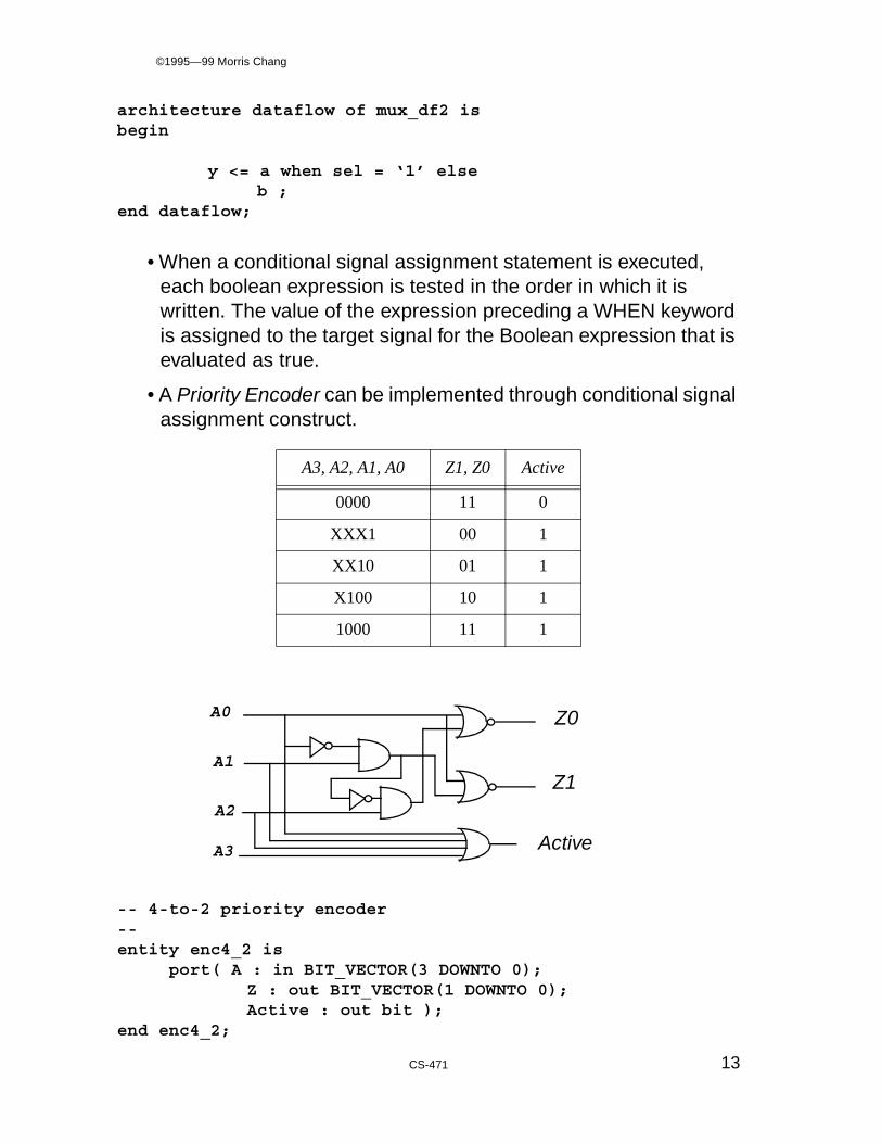
• Decoder
Decoder is another example to use the selected signal assignment construct. Consider the 3-to-8 decoder:
The decoder has a 3-bit address input and eight output lines. An output, i, becomes active (high) when the input address is equal to i.
-- three-to-one decoderlibrary ieee;use ieee.std_logic_1164.all;
entity dcd_3_8 isport( adr: in std_logic_vector(2 downto 0);
sel_out: out std_logic_vector(7 downto 0));
end dcd_3_8;
architecture dataflow of dcd_3_8 isbegin -- select is a concurrent stm which can’t be placed in a-- process
WITH adr SELECTsel_out <= “00000001” when “000”,
“00000010” when “001” | “00Z”,“00000100” when “010” | “0Z0”,“00001000” when “011” | “0ZZ”,“00010000” when “100” | “Z00”,“00100000” when “101” | “Z0Z”,“01000000” when “110” | “ZZ0”,“10000000” when “111” | “ZZZ”,“XXXXXXXX” when OTHERS;
Decodera0a1a2
s0s1s2s3s4s5s6s7

©1995—99 Morris Chang
CS-471 11
-- the ‘X’ is interpreted as 0-- The open input, ‘Z’, will be treated as logic ‘1’
end dataflow;
• The last waveform causes all bits of the output to become ‘X’, which will be interpreted as ‘0’. The use of OTHERS with the last waveform statement reduces the amount of coding if we were to list all of the possible values.
• IEEE Std 1164-1993 defines a standard logic package that allows nine values to be used to model a signal line. The nine values include:type STD_LOGIC is (
‘U’ -- Uninitialized‘X’ -- Forcing Unknown‘0’ -- Forcing Low‘1’ -- Forcing High‘Z’ -- High Impedance‘W’ -- Weak Unknown‘L’ -- Weak Low‘H’ -- Weak High‘-’ -- Don’t Care);
-- This package can be found in \maxplus2\max2vhdl\ieee
• When a gate’s output is in high-impedance state, it is considered as the gate were disconnected from the output. A tri-state buffer:
• The next example adds output enable (OE) to the 3-to-8 decoder.
-- three-to-one decoderlibrary ieee;use ieee.std_logic_1164.all;
entity dcd_38_2 isport( adr: in std_logic_vector(2 downto 0);
oe : in std_logic; sel_out: out std_logic_vector(7 downto 0));
OE
Din Dout
Din OE Dout
X01
011
Z01

©1995—99 Morris Chang
CS-471 12
end dcd_38_2;
architecture dataflow of dcd_38_2 is signal oe_adr :std_logic_vector(3 downto 0);begin
oe_adr <= oe & adr; -- concatenate signal together for SELECT
WITH oe_adr SELECTsel_out <= “00000001” when “1000”,
“00000010” when “1001” | “100Z”,“00000100” when “1010” | “10Z0”,“00001000” when “1011” | “10ZZ”,“00010000” when “1100” | “1Z00”,“00100000” when “1101” | “1Z0Z”,“01000000” when “1110” | “1ZZ0”,“10000000” when “1111” | “1ZZZ”,“ZZZZZZZZ” when others;
end dataflow;
• A bus system can be constructed with tri-state gates.
• in Maxplus2 6.01, tri-state gates must be described at top level in the hierarchy of the VHDL description.
1.3.2.3 Conditional Signal Assignment
• Conditional signal assignment statements list a series of expressions that are assigned to a target signal after the positive evaluation of one more Boolean expressions.
entity mux_df2 isport( a, b, sel : in bit;
y : out bit );end mux_df2;
bus controller
device_A device_B
8 8
8 8-bit bus
©1995—99 Morris Chang
CS-471 13
architecture dataflow of mux_df2 isbegin
y <= a when sel = ‘1’ else b ;
end dataflow;
• When a conditional signal assignment statement is executed, each boolean expression is tested in the order in which it is written. The value of the expression preceding a WHEN keyword is assigned to the target signal for the Boolean expression that is evaluated as true.
• A Priority Encoder can be implemented through conditional signal assignment construct.
-- 4-to-2 priority encoder--entity enc4_2 is
port( A : in BIT_VECTOR(3 DOWNTO 0); Z : out BIT_VECTOR(1 DOWNTO 0);
Active : out bit );end enc4_2;
A3, A2, A1, A0 Z1, Z0 Active
0000 11 0
XXX1 00 1
XX10 01 1
X100 10 1
1000 11 1
Z0
Z1
Active
A0
A1
A2
A3
©1995—99 Morris Chang
CS-471 14
architecture dataflow of enc4_2 isbegin
Z <= “00” WHEN A(0) = ‘1’ ELSE
“01” WHEN A(1) = ‘1’ ELSE “10” WHEN A(2) = ‘1’ ELSE “11”; -- when A(3) = ‘1’ or A = “0000”
Active <= ‘0’ when A = “0000” else ‘1’;end dataflow;
• An example of conditional signal assignment with multiple alternatives:
-- 4-to-1 muxentity mux2_df is
port( data : in BIT_VECTOR(3 DOWNTO 0);sel: in INTEGER RANGE 0 TO 3;f : out bit );
end mux2_df;
architecture dataflow of mux2_df isbegin
f <= data(0) WHEN sel = 0 ELSE
data(1) WHEN sel = 1 ELSE data(2) WHEN sel = 2 ELSE data(3);
end dataflow;
• For a given conditional signal assignment statement, there is an equivalent process statement that has the same semantic meaning. Such a process statement has exactly one if statement and one wait statement (or sensitivity list) within it.
entity mux isport (a, b, sel: in bit; y: out bit);end mux;
architecture behv of mux isbegin
PROCESS (a, b, sel) -- or

©1995—99 Morris Chang
CS-471 15
-- WAIT ON a, b, sel; begin
IF(sel = ‘0’) THEN y <= b; ELSIF(sel = ‘1’) THEN y <= a; END IF; END PROCESS; end behv;
• The statements appearing inside a process statement are executed sequentially. The process statements can be used to describe purely combinatorial logic or sequential logic.
1.3.3 Behavioral Description in VHDL
• The following example describes the behavior of a clock. This example may not be synthsizable under current technology.
ARCHITECTURE behavioral OF clock_component IS
BEGINPROCESS
VARIABLE periodic: BIT := ‘1’;
BEGINIF en = ‘1’ THEN
periodic := NOT periodic;END IF;
ck <= periodic;
WAIT FOR 1 US;
END PROCESS;END behavioral;

©1995—99 Morris Chang
CS-471 16
• The PROCESS statement in VHDL is used for all behavior descriptions. The syntax is similar to most of the high level languages. High level looping (e.g. for-loop) and branching (e.g. if-then-else, case ) can be used in processes.
• The statements appearing inside a process statement are executed sequentially. A process statement is a concurrent statement that can appear within an architecture body.
• It is possible to have more than one process (e.g. two FSMs) within an architecture body. These processes communicate with each other using signals that are visible to all the processes.
• Information can only be transferred between processes via signals.
• A process statement, too, has a declarative part (between the keyword PROCESS and BEGIN), and a statement part (between the keyword BEGIN and END PROCESS).
• The list of signals specified within the parenthesis after the keyword process constitutes a sensitivity list. The process statement is invoked whenever there is an event on any signal in the sensitivity list.
process ( A, B, enable)variable . . . : BIT;
begin. . .
end process;
Note: EVENT means signal change
VARIABLE periodic: BIT := ‘1’;
• The keyword VARIABLE declares a local variable (periodic) and initializes it to ‘1’. Variables cannot be declared globally.
• The := symbol is used for variables assignments while <= is used for assignments into signals. Unlike signals, variables have no direct hardware significance and have no timing associated with them.
WAIT FOR 1 US;

©1995—99 Morris Chang
CS-471 17
• In the above example, the WAIT statement causes the execution of the process to be suspended for 1 microsecond (1 US). When this time expires, the process executes again (since no sensitivity list), and complement periodic if en is ‘1’, or holds the old value of periodic if en is ‘0’.
1.3.3.1 Combinatorial Logic
• example 1entity mux isport (a, b, sel: in bit; y: out bit);end mux;
architecture behv of mux isbegin
process (a, b, sel)begin
if(sel = ‘0’) then y <= b; elsif(sel = ‘1’) then y <= a; end if; end process; end behv;
• To ensure that a process is combinatorial, its sensitivity list must contain all signals that are read in the process.
• example 2
-- example of counting the number of bits with the value 1 -- Altera VHDL p.24
library ieee;
-- for the predefined package std_logic use ieee.std_logic_1164.all;
entity proc isport( d : in std_logic_vector(2 downto 0);
q : out integer range 0 to 3);
end proc;

©1995—99 Morris Chang
CS-471 18
ARCHITECTURE proc OF proc ISBEGIN
process(d)VARIABLE num_bits : integer;
BEGIN
num_bits := 0; -- variable assignmentFOR i IN d’RANGE LOOP
IF d(i) = ‘1’ THENnum_bits := num_bits + 1;
END IF;END LOOP;
q <= num_bits;END process;
END proc;
--** EQUATIONS **
--d0 : INPUT;--d1 : INPUT;--d2 : INPUT;
--% q0 = _LC017 %-- q0 = LCELL( _EQ001 $ d2);-- _EQ001 = !d0 & d1-- # d0 & !d1;
--% q1 = _LC018 %-- q1 = LCELL( _EQ002 $ d2);-- _EQ002 = d0 & d1 & !d2-- # !d0 & !d1 & d2;
• The d’RANGE : obtains the attribute of the signal d. RANGE is a predefined attribute that returns information about signals. The single quote ( ’ ) is often read as “tick “.
• The bounds of the range for an integer type must be constants or locally static expressions; A locally static expression is an expression that computes to a constant value at compile time.

©1995—99 Morris Chang
CS-471 19
• The following example shows the non-constant index in an array (which is not synthesizable under current technology).
library ieee;use ieee.std_logic_1164.all;-- count the number of bits with the value 1 -- this example employs a sequential circuit;-- This example shows non-constant index error in synthesis
entity pro_reg2 isport( d : in std_logic_vector(2 downto 0);
clock : in std_logic; q : out integer range 0 to 3
);end pro_reg2;
entity pro_reg2 isport( d : in std_logic_vector(2 downto 0);
clock : in std_logic; q : out integer range 0 to 3
);end pro_reg2;
architecture proc of pro_reg2 issignal d_tmp : std_logic_vector(2 downto 0);
beginprocess
variable num_bits : integer;variable count : integer;
beginwait until clock’event and clock = ‘1’;d_tmp <= d; -- this stm infer the reg.num_bits := 0; count := 0; -- can be constant or non-constantfor i in d’range loop -- OK!
if d_tmp(count) = ‘1’ thennum_bits := num_bits + 1;
-- count := count + 1; -- error (non-constant -- array index)
end if; count := count + 1; -- ok! (no register is
-- inferred) -- count := count + 2; -- compile error; out of
-- array boundsend loop;

©1995—99 Morris Chang
CS-471 20
q <= num_bits; -- registers are inferred end process;
end proc;
1.3.3.2 Sequential Logic
• Registers can be implemented explicitly with Altera Macrofunction. This is done through the use of component instantiation (will be discussed later).
• A register can also be implemented implicitly with a register inference.
• Inferred D flip-flops (register) are created by Wait Statements or IF THEN ELSE statement which are surrounded by sensitivities to a clock. By detecting clock edges, the synthesis tool can locate where to insert flip-flops so that the design is built as the simulation predicts.
• Note: the wait statement must be listed at the beginning of the process statement.
• Unlike component instantiations, register inferences are technology independent, When registers are inferred, synthesis can select them from the library you are currently using.
processbegin
wait until clk = ‘1’;q <= d;
end process; -- register with active-high clock
• Register with active-high clock and asynchronous clear. The if statement is used to prioritize the statements so that the asynchronous control clr have priority over the clk signal.
process(clk,clr)begin
if clr = ‘1’ thenq <= ‘0’;
elseif clk’event and clk = ‘1’ thenq <= d;
end if;end process;

©1995—99 Morris Chang
CS-471 21
• The process with sensitivity list is assumed to contains an implicit “wait on sensitivity-list” statement as the last statement in the process.
• The process without an explicit sensitivity list, must have at least one WAIT statement, otherwise, the process will never get suspended.
• The process with an explicit sensitivity list, must not contain an explicit wait statement. Thus, it is an error to have explicit sensitivity list and a wait statement both present in a process.
process ( clk) -- error! begin
wait until clk = ‘1’;q <= d;
end process; -- register with active-high clock
• Examples of the logic with two flip-flops and one 2-to-1 mux
— No sensitivity list
--dff_mux2.vhdentity dff_mux2 is
port (reset,clock,din,sel : in std_logic;dout : out std_logic);
end dff_mux2;
architecture inference of dff_mux2 is
DQ
R
DQ
R
din q_out1
q_out2clock
dout
sel

©1995—99 Morris Chang
CS-471 22
signal q_out1, q_out2: std_logic;begin
PROCESS -- sensitivity list is not requiredbegin
WAIT UNTIL (clock’EVENT AND clock = ‘1’);q_out1 <= din;q_out2 <= q_out1;
END PROCESS;dout <= q_out1 when sel = ‘1’ else
q_out2;end inference;
** EQUATIONS ** synthesis results
clock : INPUT;din : INPUT;sel : INPUT;
% dout = _LC017 % dout = LCELL( _EQ001 $ GND); _EQ001 = q_out1 & sel # q_out2 & !sel;
% q_out1 = _LC018 %q_out1 = DFFE( din $ GND, clock, VCC, VCC, VCC);
% q_out2 = _LC019 %q_out2 = DFFE( q_out1 $ GND, clock, VCC, VCC, VCC);
Note: DFFE is a DFF primitive with clock Enable in the Altera library. DFFE ( d, clk, clrn, prn, q, ena). The equivalent symbol is
DQ
PRN
CLRN
ENA

©1995—99 Morris Chang
CS-471 23
— with sensitivity list
-- filename dff_mux3.vhd
entity dff_mux3 isport (reset,clock,din,sel : in std_logic;
dout : out std_logic);
end dff_mux3;
architecture inference of dff_mux3 issignal q_out1, q_out2: std_logic;
beginprocess(reset,clock) -- sensitivity list requiredbegin
if (reset = ‘1’) then q_out1 <= ‘0’; q_out2 <= ‘0’;elsif (clock’event and clock = ‘1’) then q_out1 <= din; q_out2 <= q_out1;end if;
end process;dout <= q_out1 when sel = ‘1’ else
q_out2;end inference;
** EQUATIONS **
clock : INPUT;din : INPUT;reset : INPUT;sel : INPUT;
% dout = _LC017 % dout = LCELL( _EQ001 $ GND); _EQ001 = q_out1 & sel # q_out2 & !sel;
% q_out1 = _LC018 %q_out1 = DFFE( din $ GND, clock, !reset, VCC, VCC);
% q_out2 = _LC019 %q_out2 = DFFE( q_out1 $ GND, clock, !reset, VCC, VCC);

©1995—99 Morris Chang
CS-471 24
— including preset in the sensitivity list
entity dff_mux4 isport (reset,preset,clock,din,sel : in std_logic;
dout : out std_logic);
end dff_mux4;
architecture inference of dff_mux4 issignal q_out1, q_out2: std_logic;
beginprocess(preset,reset,clock)begin
if (reset = ‘1’) then q_out1 <= ‘0’; q_out2 <= ‘0’;elsif (preset = ‘1’) then q_out1 <= ‘1’; q_out2 <= ‘1’;elsif (clock’event and clock = ‘1’) then q_out1 <= din; q_out2 <= q_out1;end if;
end process;dout <= q_out1 when sel = ‘1’ else
q_out2;end inference;
** EQUATIONS **
clock : INPUT;din : INPUT;preset : INPUT;reset : INPUT;sel : INPUT;
% dout = _LC017 % dout = LCELL( _EQ001 $ GND); _EQ001 = q_out1 & sel # q_out2 & !sel;
% q_out1 = _LC018 %q_out1 = DFFE( din $ GND, clock, !reset, !preset, VCC);

©1995—99 Morris Chang
CS-471 25
% q_out2 = _LC019 %q_out2 = DFFE( q_out1 $ GND, clock, !reset, !preset,VCC);
Latches
• Latches can be produced when omitting the ELSE statement in the “IF-THEN-ELSE” construct in a process.
— For example, a latch is inferred in the following process.
process (en, data_in)begin
if (en = ‘1’)thendata_out <= data_in;
end if;end process;
— A latch is a level sensitive memory device; a flip-flop is an edge-triggered memory device.
• For example, a 3-input OR-AND2 function can be written to contain
— no latch,
— one latch
— two latches
entity orand is port(a,b,c : in bit; z : out bit );end orand;architecture a of orand isbegin orand3: process(a,b,c) begin
2. Al Graf, “Harness the power of VHDL for PLD design”, Electronic Design, Sep. 19, 1994
D Q
en
data_in data_out
enlatch

©1995—99 Morris Chang
CS-471 26
if(c = ‘1’ ) then if (a = ‘1’ or b = ‘1’) then z <= ‘1’;
else z <= ‘0’; -- inner else end if;
else z <= ‘0’; -- outer else end if; end process;end;
• in case (b): the VHDL code implied that the last value of signal z will be saved (in a memory element) until the next occurrence of the condition (c = 1 ) that satisfies the IF-THEN statement.
• in case (c): the output of the OR gate will be changed to 1 when (a = 1 or b = 1), and the value should be held until the condition is met again.
• To avoid inadvertently creating implied latches, the else statement should always be paired with if statement.
abc z
a
bc
z
abc z
latch a
bc
z
ab
c
z
latchlatch a
bc
z
omission of the outer else
omission of both else
(a)
(b)
(c)

©1995—99 Morris Chang
CS-471 27
1.3.3.3 Bidirectional Bus with tri-state buffer
• The data bus of a microprocessor is a bidirectional bus. Such bus can, for example, fetch data (or instructions) from, or store data back to, external devices. The following example depicts the use of tri-state buffer in a bidirectional bus structure.
• schematic and the corresponding VHDL code
-- bidirectional bus with tri-state buffer -- Filename : triBuf.vhd-- (c)1997 Morris Chang-- Note: During the simulation stage, be sure to set the -- iobus [input mode] to Z (from SCF) when the ena = ‘1’-- (since the iobus is driven by the myBuf). --
LIBRARY IEEE;USE ieee.std_logic_1164.ALL;
ENTITY triBuf IS PORT( iobus : INOUT std_logic; i1,i2,ena, clk,reset: IN std_logic; o3 : OUT std_logic);END triBuf;
ARCHITECTURE data OF triBuf IS SIGNAL is1 : std_logic;BEGIN
is1 <= i1 and i2;
MyReg: PROCESS(clk,iobus,reset) BEGIN IF (reset = ‘1’) then o3 <= ‘0’;
o3D
clkiobus
ena myBuf
myReg
is1
i1i2

©1995—99 Morris Chang
CS-471 28
elsif (clk = ‘1’ and clk’event) THEN o3 <= iobus; END IF; END PROCESS; Mybuf: PROCESS(ena,is1,iobus) BEGIN IF (ena = ‘1’) THEN iobus <= is1; else iobus <= ‘Z’; END IF; END PROCESS;END data;
• The tri-state buffer is inferred in the process — Mybuf.
• During the simulation, there are two channels for the bidirectional pin (i.e. iobus): one for input mode and one for output mode. As the bidirectional pin performs output function, the channel for input mode must be set to high impedance (i.e. Z).
1.3.4 Finite State Machine
• Finite state machines (FSM) can usually be described using a case statement in a process. The state information is stored in a signal.
• The state encoding (e.g. one-hot) can be explicitly defined through PLD vender-specific attribute (e.g enum_encoding in Altera.)
1.3.4.1 Finite State Machine and Asynchronous Input
• ASM chart (Algorithmic State Machine Chart)

©1995—99 Morris Chang
CS-471 29
— States
— Conditional branch
— conditional output
state_name
state_X
clock
stateX
W_out
note: W_out is a unconditional outputW_out is a logic value “1” in the state X
din = 1FT
W_out
©1995—99 Morris Chang
CS-471 30
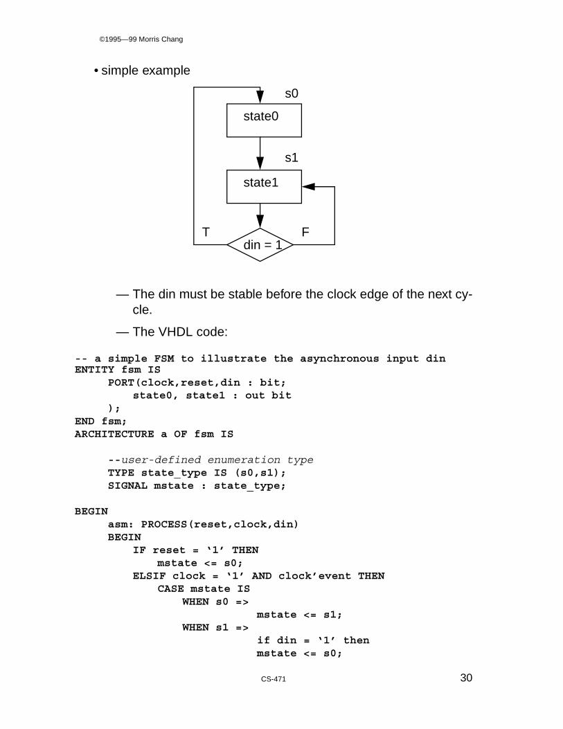
• simple example
— The din must be stable before the clock edge of the next cy-cle.
— The VHDL code:
-- a simple FSM to illustrate the asynchronous input dinENTITY fsm IS
PORT(clock,reset,din : bit;state0, state1 : out bit
);END fsm;ARCHITECTURE a OF fsm IS
--user-defined enumeration type TYPE state_type IS (s0,s1);SIGNAL mstate : state_type;
BEGINasm: PROCESS(reset,clock,din)BEGIN
IF reset = ‘1’ THENmstate <= s0;
ELSIF clock = ‘1’ AND clock’event THENCASE mstate IS
WHEN s0 =>mstate <= s1;
WHEN s1 =>if din = ‘1’ thenmstate <= s0;
s0
s1
din = 1FT
state0
state1

©1995—99 Morris Chang
CS-471 31
end if;END CASE;
END IF;END PROCESS;
state0 <= ‘1’ WHEN mstate = s0 ELSE ‘0’;-- concurrent state1 <= ‘1’ WHEN mstate = s1 ELSE ‘0’;-- concurrent
END a;
• The state machine is implemented through CASE-WHEN statement in the process asm . The output signals are decoded from state variable mstate (through concurrent statements.)
• The VHDL feature — enumerated types, which allows the data type used for the state variable (i.e. mstate) to be defined as alphanumeric elements, makes the code more readable.
— s0, s1 are enumeration literals.
— The order of values appearing in an enumeration type dec-laration defines the lexical order for the values. For example, (s0 < s1) expression returns a TRUE while (s0 > s1) returns FALSE.
— Values of an enumeration type also have a position number associated with them. The position number of the leftmost element is 0.
— The default initial value is the left-most enumeration literals.
SIGNAL mstate : state_type;
-- the mstate has initial value as s0
• How many registers are inferred in this design ?
• The value of the output state0 becomes 1 as the state machine is in the s0 state.
• What if the output-signal assignments were placed inside the process asm ?
CASE mstate ISWHEN s0 =>
state0 <= ‘1’;

©1995—99 Morris Chang
CS-471 32
state1 <= ‘0’;mstate <= s1;
WHEN s1 =>state0 <= ‘0’;state1 <= ‘1’;if din = ‘1’ thenmstate <= s0;end if;
END CASE;
— This design will affect the efficiency and the timing.
— Two more registers are inferred for the control outputs state0 and state1 which are placed within the synchronous process asm. Registers often are the limiting factor in the design fitting process of the PLD design environ-ment.
— The outputs state0 and state1 change value one cycle after the state transition.
1.3.4.2 Interaction Between Two Processes
• We will add one more process to the FSM example illustrated in previous section.
• Alternatively, the output decoding part can be placed in a separate, independent combinatorial process which will be run parallel to the process asm.
decoder: process if(mstate = s0) then
state0 <= ‘1’; state1 <= ‘0’;else
state0 <= ‘0’; state1 <= ‘1’;end if;
end process;
• Information can only be transferred between processes (e.g. asm and decoder) via signals ( e.g. mstate.)

©1995—99 Morris Chang
CS-471 33
1.3.4.3 From ASM chart to VHDL
• Given an ASM chart as follows,
X,Y
AF
B
X
WB
F
F
TT
Y
B,C00
J
K
NM
L
W
1-
01
ASM Chart
000
001
010
100011
RST

©1995—99 Morris Chang
CS-471 34
• The expected timing diagram (zero delay)
• The VHDL code,
J K N M J K L M M K N M
T
F
T
F
T
F
T
F
T
F
T
F
ck
Sample Timing Diagram

©1995—99 Morris Chang
CS-471 35
-- This example show how to translate a given ASM chart toVHDL-- The filnname : asm2.vhd-- Note: the inputs a, b and c are asynchronous input.-- Author: M. Chang (Illinois Institute of Technology)
entity asm2 is -- Specify the inputs and outputs port(
clock, reset:IN bit;a,b,c :IN bit;x_out,y_out,w_out:OUT bit ;state :OUT bit_vector(4 downto 0)
-- NOTE: output state variables );
end asm2;
architecture statemach of asm2 is
type state_type is (j,k,l,m,n);signal mstate, next_state : state_type;
-- initial state is jBEGIN
state_register: process(clock,reset) begin if reset = ‘1’ then
mstate <= j;elsif clock’event and clock = ‘1’ then
mstate <= next_state;end if;end process;
state_logic: process(mstate,a,b,c) begin
x_out<= ‘0’;y_out <= ‘0’;w_out <= ‘0’;
CASE mstate ISWHEN j =>
next_state<= k;WHEN k =>
x_out <= ‘1’;y_out <= ‘1’;IF a = ‘1’ THEN next_state<= l;ELSIF (a = ‘0’ and b = ‘1’) THEN next_state<= n;
w_out <= ‘1’;

©1995—99 Morris Chang
CS-471 36
ELSIF (a = ‘0’ and b = ‘0’) THEN next_state<= n;END IF;
WHEN l =>x_out <= ‘1’;IF b = ‘0’ THEN w_out <= ‘1’;
else w_out <= ‘0’; end if;IF b = ‘1’ THEN next_state<= m;ELSE next_state<= n;END IF;
WHEN m =>w_out <= ‘1’;IF b = ‘1’ THEN next_state<= m;ELSIF ( b = ‘0’ and c = ‘1’) THEN next_state<= k;ELSIF ( b = ‘0’ and c = ‘0’) THEN next_state<= j;END IF;
WHEN n =>next_state<= m;y_out <= ‘1’;
END CASE;
end process;
with mstate selectstate <= “00001” when j,
“00010” when k, “00100” when l, “01000” when m, “10000” when n;
END statemach;
1.3.5 Structural Description in VHDL
• A digital system, very often, is described as a set of components connected by signals. The implementation detail of components are not known at this level. The interface of the components, however, must be explicitly declared.

©1995—99 Morris Chang
CS-471 37
• The components are instantiated in the architecture body via component instantiation statements.
• Structural description establishes the hierarchy in a design description.
• The following example illustrates the structural description of a 4-to-1 mux.
ENTITY mux2con is PORT ( data : in bit_vector(3 downto 0); sel: in bit_vector(1 downto 0); f : out bit );END mux2con; ARCHITECTURE structural of mux2con is
COMPONENT mux port ( a,b,sel : in bit; y : out bit);
END COMPONENT;FOR ALL : mux USE ENTITY work.mux (behv);-- optionalsignal ins1, ins2 : bit;
BEGINm1: mux PORT MAP(data(3), data(2), sel(0), ins1);m2: mux PORT MAP(data(1), data(0), sel(0), ins2);m3: mux PORT MAP(ins1, ins2, sel(1), f);
END structural;
• The architecture body has declarative part and statement part.
AB
Sel
Y
AB
Sel
Y
AB
Sel
Y
m1
m2
data(3)
data(2)
data(1)data(0)sel(0)
sel(1)
f
ins1
ins2
m3
mux2con

©1995—99 Morris Chang
CS-471 38
• Declarative part includes (1) the name of the component and its ports (i.e. component declaration) (2) the name of the internal signal which will be used in the architecture. The scope of the signals is restricted to the architecture body (will not be recognized outside the body). The internal signal ins1 is used as a carrier for connecting two components. (3) the configuration specifications.
FOR ALL : mux USE ENTITY work.mux (behv);
• The configuration of mux specifies that for all instantiations of this component (ALL : mux) the behv architecture of the mux entity (which exists in the WORK library) should be used. By default (i.e. without the configuration specifications), the Altera system will pick up the component (i.e. mux) from the current directory.
• Statement part has the instantiation of the components declared in the declarative part. The m1 ( or m2, m3) is the component label for the component instantiated. The interconnections of components are described here.
• Signals in the instantiations will be mapped to the ports of the instantiated component according to their ordering in the port map list (called positional association). For example, in m1,
• Name association (i.e. ports are mapped directly to signals regardless of the order in which they are listed) can be quite useful for the interconnection of buses.
m1: mux PORT MAP(data(3), data(2), sel(0), ins1);
Can be rewritten to
m1: mux PORT MAP( b=>data(2), a=>data(3), sel=>sel(0), y=>ins1);
data(3)
a
data(2)
b
sel(0)
sel
ins1
y
externalsignal:internalsignal:

©1995—99 Morris Chang
CS-471 39
• A component instantiation statement is a concurrent statement. Thus the order of these statements is not important.
1.3.6 Structural Description with Library
• PLD vendors have their own basic functional blocks (i.e. primitives) used in circuit designs. The Component Declaration for these primitives are usually provided through a package which placed in vendor-specific library.
• The primitives such as flip-flop (e.g. DFF, DFFE, JKFF, JKFFE ... etc) can be accessed explicitly through component instantiation. This approach, however,
— must include the library and package in your VHDL code
— becomes technology dependent (vendor dependent), thus, may affect the portability of your VHDL code.
• Alternative implementation of the example with two DFF and one mux is described as follows. This example uses Altera’s maxplus2 package. This package is located in /maxplus2/max2vhdl/altera/maxplus2.vhd.
LIBRARY altera; use altera.maxplus2.all;-- /maxplus2/max2vhdl/altera/maxplus2.vhdLIBRARY ieee;USE ieee.std_logic_1164.all;
entity dff_mux1 isport (reset,clock,din,sel : in std_logic;
dout : out std_logic);
end dff_mux1;
architecture synth of dff_mux1 issignal clearn, presetn, q_out1, q_out2: std_logic;
BEGINclearn<= not reset;presetn<=’1’;
-- logic values ‘1’ are equivalent to the VCC primitives
r1 : dff PORT MAP (d=>din, q=>q_out1,clk=>clock,
©1995—99 Morris Chang
CS-471 40
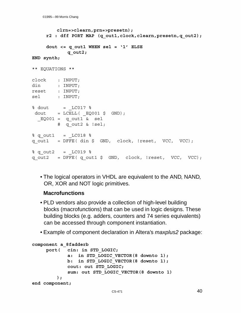
clrn=>clearn,prn=>presetn);r2 : dff PORT MAP (q_out1,clock,clearn,presetn,q_out2);
dout <= q_out1 WHEN sel = ‘1’ ELSEq_out2;
END synth;
** EQUATIONS **
clock : INPUT;din : INPUT;reset : INPUT;sel : INPUT;
% dout = _LC017 % dout = LCELL( _EQ001 $ GND); _EQ001 = q_out1 & sel # q_out2 & !sel;
% q_out1 = _LC018 %q_out1 = DFFE( din $ GND, clock, !reset, VCC, VCC);
% q_out2 = _LC019 %q_out2 = DFFE( q_out1 $ GND, clock, !reset, VCC, VCC);
• The logical operators in VHDL are equivalent to the AND, NAND, OR, XOR and NOT logic primitives.
Macrofunctions
• PLD vendors also provide a collection of high-level building blocks (macrofunctions) that can be used in logic designs. These building blocks (e.g. adders, counters and 74 series equivalents) can be accessed through component instantiation.
• Example of component declaration in Altera’s maxplus2 package:
component a_8fadderbport( cin: in STD_LOGIC;
a: in STD_LOGIC_VECTOR(8 downto 1);b: in STD_LOGIC_VECTOR(8 downto 1);cout: out STD_LOGIC;sum: out STD_LOGIC_VECTOR(8 downto 1)
);end component;

©1995—99 Morris Chang
CS-471 41
1.3.7 Structural Description with User-Defined Macrofunctions
• Building user-defined macrofunctions is desirable in the hierarchical design approach.
• When instantiating user-defined macrofunctions, the ports of the macrofunction with a component declaration must be specified. This component declaration can be placed in a package (in a separate file) which, then, will be declared (with a use clause) in the top-level design file.
Example (with the package construct)
— the component declaration is placed in file mux_pak.vhd :
-- my mux_pak package
PACKAGE mux_pak IS component mux port ( a,b,sel : in bit; y : out bit); end component;END mux_pak;
— the top-level design file mux2pkg.vhd :
-- use of user-defined package LIBRARY work; -- work library is the default libraryUSE work.mux_pak.all; -- in the file: mux_pak.vhd entity mux2pkg is port ( data : in bit_vector(3 downto 0); sel: in bit_vector(1 downto 0); f : out bit );end mux2pkg;
ARCHITECTURE struc OF mux2pkg ISsignal ins1, ins2 : bit;
BEGINm1: mux port map(data(3), data(2), sel(0), ins1);m2: mux port map(data(1), data(0), sel(0), ins2);m3: mux port map(ins1, ins2, sel(1), f);
END struc;

©1995—99 Morris Chang
CS-471 42
• The macrofunctions (e.g. the design of mux) must be compiled before it can be used as components in the higher-level design.
2. More VHDL examples
2.1 Adders
• Full adder (filename full_add.vhd)
ENTITY full_add is port(a,b,cin : in bit; sum,cout: out bit);end full_add; architecture df of full_add isbegin cout <= (a and b) or (a and cin) or (b and cin); sum <= (a xor b) xor cin;end df;
• Full adder using function construct (filename fadd_fcn.vhd )
ENTITY fadd_fcn is port(a,b,cin : in bit; sum,cout: out bit);end fadd_fcn; architecture df of fadd_fcn is
-- following is a function body FUNCTION f_cout(a,b,cin : in bit) RETURN bit IS BEGIN RETURN (a and b) or (a and cin) or (b and cin);
END f_cout;
begin-- function call with positional association
cout <= f_cout(a,b,cin); sum <= (a xor b) xor cin;end df;
• The general syntax for a function body:

©1995—99 Morris Chang
CS-471 43
function function_name (parameter_list) return return_type is
begin . . . end function_name;
• The only mode allowed for the parameters is mode in. Also, only constants and signal objects can be passed in as parameters. The default object class is constant (e.g. a, b, cin).
• Using function in a signal assignment:
cout <= f_cout(a,b,cin);
• The function body can be placed in a package body which is always associated with a package declaration.
package declaration and package body:(filename : my_pkgbd.vhd )
-- package body for Full Adder using function
PACKAGE my_pkgbd IS FUNCTION f_cout(a,b,cin : in bit) RETURN bit;END my_pkgbd; PACKAGE BODY my_pkgbd IS -- following is a function body FUNCTION f_cout(a,b,cin : in bit) RETURN bit IS BEGIN RETURN (a and b) or (a and cin) or (b and cin); END f_cout;END my_pkgbd;
The full adder uses package my_pkgbd ( filename: fa_pkgbd.vhd)
library work;use work.my_pkgbd.all; ENTITY fa_pkgbd is port(a,b,cin : in bit; sum,cout: out bit);END fa_pkgbd; architecture df of fa_pkgbd isbegin

©1995—99 Morris Chang
CS-471 44
-- function call with positional association cout <= f_cout(a,b,cin); sum <= (a xor b) xor cin;end df;
• It is worth noting that a package body is not necessary if the corresponding package declaration has no function (or procedure, deferred constant) declarations.
• Building an 8-bit ripple adder — a cascade of 8 full-adder stages, each of which handles one bit.
• Apparently, the above design presents a very good regularity in the signal interconnections. We will use two instances of full_add for the first and last bits of the adder. The rest of the bits are instantiated in an iterative fashion to take advantage of the VHDL generate statement.
• 8-bit adder (filename fadd8.vhd)
ab
cinsumcout
a(0)b(0)
ab
cinsumcout
a(1)b(1)
ab
cinsumcout
a(7)b(7)
ab
cinsumcout
a(6)b(6)
sum(0)
sum(1)
sum(6)
sum(7)
im(0)
im(1)
im(5)
im(6)
cout
cin

©1995—99 Morris Chang
CS-471 45
ENTITY fadd8 is port(a,b : in bit_vector(7 downto 0); cin : in bit; sum : out bit_vector(7 downto 0); cout: out bit);
CONSTANT n: integer := 8; -- constant declarationend fadd8; architecture iterative of fadd8 is component full_add port (a,b,cin: in bit; sum, cout: out bit); end component; -- CONSTANT n: integer := 8;-- constant declaration signal im: bit_vector(0 to n-2);begin g0: full_add port map(a(0), b(0), cin, sum(0), im(0)); g1to6: FOR i IN 1 TO n-2
GENERATE g: full_add port map(a(i),b(i),im(i-1),
sum(i),im(i)); END GENERATE;
gn: full_add port map(a(n-1),b(n-1),im(n-2),sum(n-1),cout);
end iterative;
• The GENERATE statement labeled g1to6 is used for wiring the full adders for bits 1 to 6. A FOR loop with index i changing from 1 to n-2 are used in the GENERATE statement.
• The generate statement, works like a macro expansion, is interpreted during elaboration. It provides for a compact description of regular structures such as memories, registers, and counters.
• There are two forms of the generate statement.
— for-generation scheme: must have locally static bounds (to be synthesizable.)
— if-generation scheme: must have locally static conditions (to be synthesizable.)
Note: A locally static expression is an expression that computes to a constant value at compile time.

©1995—99 Morris Chang
CS-471 46
• The if-generate statement is quite useful in handle the boundary conditions in repetitive structures. An if-generate statement does not have an else or else-if branch.
• By changing the value of the CONSTANT n, an N-bit ripple adder can be easily implemented from this design.
• Design reuse, an effective way to reduce the design cycles, can be achieved through parameterized design.
2.2 Design Parametrization
• GENERIC statement in VHDL can be used for parameterized design. (maxplus2 7.2, released 3/97, supports generic)
— Usage of generic parameters and passing of values to these parameters is done in much the same way as it is with ports. The syntax of constructs related to ports and gener-ics are similar.
— The eight-bit adder now is implemented with generic con-struct (file name: adder_n.vhd)
-- Morris Chang-- N-bit Adder using Generic
ENTITY adder_n isgeneric (N : integer := 8);
-- generic (N : integer ); -- the defaut value can be defined thru local generic
port(a,b : in bit_vector(N-1 downto 0); cin : in bit;
sum : out bit_vector(N-1 downto 0); cout: out bit);
-- constant n: integer := 8;end adder_n;
architecture iterative of adder_n iscomponent
full_add port (a,b,cin: in bit; sum, cout: out bit);end component;signal im: bit_vector(0 to N-2);
beging0: full_add port map(a(0), b(0), cin, sum(0), im(0));g1to6: for i in 1 to N-2

©1995—99 Morris Chang
CS-471 47
generateg: full_add port map(a(i),b(i),im(i-1),sum(i),im(i));
end generate;g2: full_add port map(a(N-1),b(N-1),im(N-2),
sum(N-1),cout); end iterative;
— The generic parameter N (the width of the adder) has a de-fault value of 8.
— In the following example, a component with generic parame-ter is instantiated to a four-bit adder. (file name adder_4.vhd)
----ENTITY adder_4 IS port(a,b : in bit_vector(4-1 downto 0); cin : in bit; sum : out bit_vector(4-1 downto 0); cout: out bit);end adder_4;
architecture simple of adder_4 is component adder_n generic (n : integer:=8);-- generic (n : integer:=8); local generic is defined
port(a,b : in bit_vector(n-1 downto 0);cin : in bit;
sum : out bit_vector(n-1 downto 0);cout: out bit);
end component; begin
g0: adder_n generic map(4) -- passing parameter port map(a, b, cin, sum, cout);
end simple;
— The absence of a generic map aspect from its instantiation implies that all such generics will use the default values (i.e. for a eight-bit adder)
g0: adder_n port map(a, b, cin, sum, cout);

©1995—99 Morris Chang
CS-471 48
— Same as port map, generic map can use either name asso-ciation or positional association.
• Library of Parameterized Modules (LPMs)
— Obviously, time to market is an important driving force be-hind the acceptance of HDLs, synthesis and CPLD. But in addition to time-to-market benefits, top-down methods promise device independence.
— Most synthesis and silicon vendors support the library of Parameterized Modules (LPMs), a set of logic functions that can be imported into a design and fit directly into the target device. This portable code concept means that you can switch silicon vendors without having to rewrite your design.
— VHDL versions of Altera’s description of LPM blocks can be found in http://www.edif.org. (“Programmable logic and syn-thesis strive to get in sync”, by Mike Donlin, Computer De-sign, August, 1996, pp78)
LIBRARY ieee;USE ieee.std_logic_1164.ALL;LIBRARY lpm;USE lpm.lpm_components.ALL
ENTITY mux_ex ISport (
data : IN STD_LOGIC_VECTOR (1 downto 0);sel :: IN STD_LOGIC_VECTOR (0 downto 0);result : OUT STD_LOGIC_VECTOR (0 downto 0)
);END mux_ex;
architecture lpm of mux_ex isBEGIN
mymux : lpm_mux -- use name associationgeneric map (LPM_SIZE => 2,
LPM_WIDTHS => 1,LPM_PIPELINE => 0, -- can be omittedLPM_width => 1)
port map (data(0,0) => data(0),data(1,0) => data(1),sel => sel,result => result);

©1995—99 Morris Chang
CS-471 49
END lpm;
•Note:LPM_WIDTH: Width of the data[ ][ ] and result[ ] ports.LPM_WIDTHS: Width of the sel[ ] input port.LPM_SIZE : Number of input buses to the multiplexer.
LPM_SIZE <= 2LPM_WIDTHS LPM_PIPELINE: Specifies the number of Clock cycles of latency associated with the result[ ] output. A value of zero (0) indicates that no latency exists, and that a purely combinatorial function will be instantiated. If omitted, the default is 0.
2.3 Counter
• Example for counter:
ENTITY counter ISPORT( din : IN INTEGER RANGE 0 TO 15;
clk : IN BIT;clear, load: INBIT;result : OUT INTEGER RANGE 0 TO 15
);end counter;
architecture behv of counter is-- A synchronous load, clear counterbegin
PROCESS (clk,load,clear)VARIABLE cnt: INTEGER RANGE 0 TO 15;
BEGINIF (clk’EVENT AND clk = ‘1’) THEN
IF clear = ‘1’ THEN -- active low may save you one gate
cnt := 0;ELSIF load = ‘1’ THEN
cnt := din;ELSE
cnt := cnt + 1;END IF;
END IF;result<=cnt;
END PROCESS;end behv;

©1995—99 Morris Chang
CS-471 50
** EQUATIONS **
clear : INPUT;clk : INPUT;din0 : INPUT;din1 : INPUT;din2 : INPUT;din3 : INPUT;load : INPUT;
% result0 = cnt0~78 %% cnt0~78 = _LC018 % result0 = DFFE( _EQ001 $ !clear, clk, VCC, VCC, VCC); _EQ001 = !clear & !load & result0 # !clear & !din0 & load;
% result1 = cnt1~78 %% cnt1~78 = _LC019 % result1 = DFFE( _EQ002 $ !clear, clk, VCC, VCC, VCC); _EQ002 = !clear & !load & result0 & result1 # !clear & !load & !result0 & !result1 # !clear & !din1 & load;
% result2 = cnt2~78 %% cnt2~78 = _LC020 % result2 = DFFE( _EQ003 $ GND, clk, VCC, VCC, VCC); _EQ003 = !clear & !load & result0 & result1 & !result2 # !clear & !load & !result1 & result2 # !clear & !load & !result0 & result2 # !clear & din2 & load;
% result3 = cnt3~78 %% cnt3~78 = _LC022 % result3 = DFFE( _EQ004 $ !clear, clk, VCC, VCC, VCC); _EQ004 = !clear & !load & result0 & result1 & result2 &result3 # !clear & !load & !result3 & _X001 # !clear & !din3 & load; _X001 = EXP( result0 & result1 & result2);
2.4 A shift register
-- 4 bit shift register with load library ieee;

©1995—99 Morris Chang
CS-471 51
use ieee.std_logic_1164.all;
entity shif_reg isport( din : in std_logic_vector(3 downto 0);
clock,load,left_right : in std_logic; dout : out std_logic_vector(3 downto 0));
end shif_reg;
architecture synth of shif_reg issignal shift_tmp : std_logic_vector(3 downto 0);
beginprocess (clock,load)begin if load = ‘1’ then -- asynchronouns load
shift_tmp <= din;elsif (clock’event and clock = ‘1’) then if (left_right = ‘0’) then -- right shift
shift_tmp <= ‘0’ & shift_tmp(3 downto 1); else
shift_tmp <= shift_tmp(2 downto 0) & ‘0’; end if;end if;
end process;dout <= shift_tmp;
end synth;
• The operands for & (concatenation) operators can be either a 1-dimensional array type or an element type. The result is always an array type. For example,
‘1’ & ‘0’
results in an array of characters “01”.
if x_byte and y_byte are two 8-bit arrays of BITs,
0 0123
0123
shift_tmp
right shift
00123
0123
shift_tmp
left shift

©1995—99 Morris Chang
CS-471 52
x_byte & y_byte
forms a 16-bit array of BITs.
Note: & operator is useful for merging buses and registers.
2.5 Building a Multiplier
• The FSM for a shift-add multiplier with one-hot state encoding.
— ASM chart
— the VHDL code (filename: mult_fsm.vhd )
LIBRARY ieee;USE ieee.std_logic_1164.all;
entity mult_fsm is
port ( clock, reset: in bit; init_out, add_out, shift_out: out bit; done: inout bit; mpl : in std_logic_vector(3 downto 0); mplr_bit : out std_logic );end mult_fsm; architecture statmach of mult_fsm is
init
add
count = nFT
init_out
add_out
shift_out
shift

©1995—99 Morris Chang
CS-471 53
constant n: integer :=4; -- for 4 bit mult_fsm type state_type is (init, add, shift);-- one hot encoding is used through attribute enum_encoding-- yes, I wasted one flip-flop
attribute enum_encoding : string;attribute enum_encoding of state_type: type is
“100 010 001”; signal mstate : state_type; -- initial state is init signal mplr_tmp : std_logic_vector(3 downto 0);begin process(clock,reset) variable count : integer range 0 to n;
-- infered registers begin if reset = ‘1’ then mstate <= init; -- asynchronous input mplr_tmp <= mpl; elsif clock = ‘1’ and clock’event then case mstate is when init =>
count := 0;mplr_bit <= mplr_tmp(0);mplr_tmp <= mplr_tmp(0)&mplr_tmp(n-1 downto 1);mstate <= add;done <= ‘0’;
when add => mstate <= shift; when shift =>
count := count +1; if (count = n) then
done <= ‘1’; --the done signal will be set in next cycle
mstate <= init; else mstate <= add; mplr_bit <= mplr_tmp(0);
mplr_tmp <= mplr_tmp(0)&mplr_tmp(n-1 downto1); end if; end case; end if; end process;
add_out <= ‘1’ when mstate = add else ‘0’;init_out <= ‘1’ when mstate = init else ‘0’;shift_out <= ‘1’ when ((mstate = shift)
and (done /= ‘1’)) else ‘0’;end statmach;

3. Programmable Logic Device
3.1 Field Programmable Gate Array (FPGA)
• Segment of the Xilinx chip architecture
— Fixed arrays of logical function cells (a.k.a. CLB — Config-urable Logic Blocks) are connectible by a system of pass transistors driven by static RAM cells.
— The RAM cells sprinkled through out the chip (define the connectivity) and are linked into a long shift register.
— The device down load the program from a serial PROM, from a microprocessor, or from a parallel PROM. This re-sults a fast reprogrammability but loses its program each time it is powered down.
• Xilinx supports three methods of interconnecting the CLBs and IOBs
— (1). Direct interconnect: Adjancent CLBs are wired together in the horizontal or vertical direction. (This is the most effi-cient interconnect) In the 3000 series — X output connect to
IOB
CLB
IOBIOB
IOB
IOB
IOB
IOB
IOB
CLBCLB
CLB
Wiring Channels

©1995—99 Morris Chang
CS-471 55
the east and west neighbors and Y output connect to the north and south neighbors. Shift registers fit nicely in this in-terconnect.
— (2). General-purpose interconnect: This are used mainly for longer distance connections or for signals with a moderate fan-out.
— (3). Long line interconnect: This are saved for time critical signals (e.g. clock signal need be distributed to many CLBs)
• 2000, 3000 and 4000 series.
— 3020: 64 LOBs and 64 CLBs (8X8 matrix) has about 2000 equivalent gates.
— 3090: 320 CLBs and 144 IOBs has about 9000 equivalent gates.
• The CLB in 3000 family.
DIBCKE
CLB0
X
Y
CE A
D R
DIBCKE
CLB1
X
Y
CE A
D R
DIBCKE
CLB2
X
Y
CE A
D R
DIBCKE
CLB3
X
Y
CE A
D R
SwitchingMatrix
Global VerticalLong Lines
Long Line
GeneralPurpose Lines
HorizontalLong Line
DirectConnections
©1995—99 Morris Chang
CS-471 56
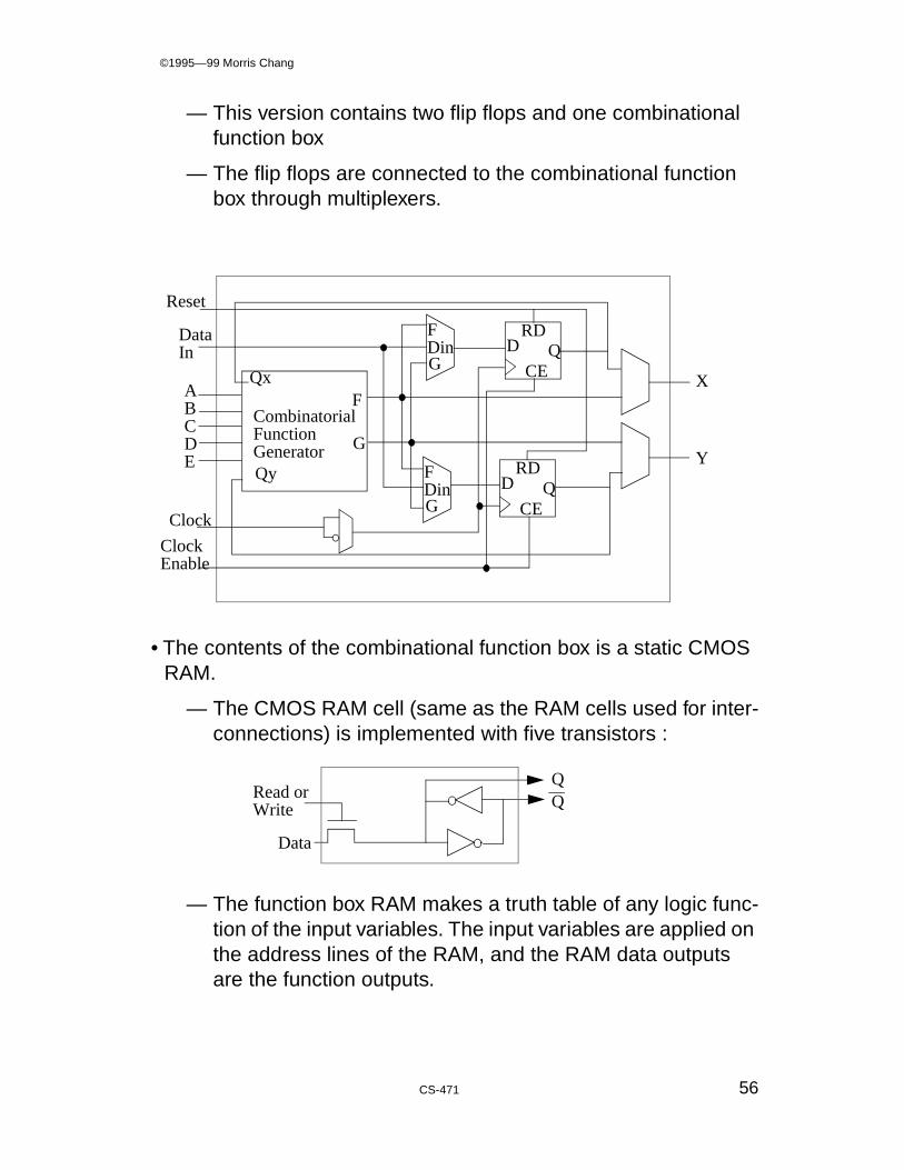
— This version contains two flip flops and one combinational function box
— The flip flops are connected to the combinational function box through multiplexers.
• The contents of the combinational function box is a static CMOS RAM.
— The CMOS RAM cell (same as the RAM cells used for inter-connections) is implemented with five transistors :
— The function box RAM makes a truth table of any logic func-tion of the input variables. The input variables are applied on the address lines of the RAM, and the RAM data outputs are the function outputs.
CombinatorialFunction Generator
Qx
Qy
F
G
ABCDE
FDinG
FDinG
RD
CE
D Q
RD
CE
D Q
Clock
ClockEnable
Data In
Reset
X
Y
Read orWrite
Data

©1995—99 Morris Chang
CS-471 57
— Exampls of RAM based truth table functions with three vari-ables A, B, C as address
3.2 Complex Programmable Logic Device (CPLD)
• Altera pioneered the developement of erasable programmable logic devices (EPLDs) based on CMOS erasable ROM technology. The EPLD can be erased by exposing it to ultraviolet (UV) light. (The newer EPLD based on EEPROM (electrically erasable PROM) technology can be erased by applying voltage to it. )
• Today, the term CPLD (Complex Programmable Logic Devices) is more popular than the term EPLD.
• The arhitecture of Altera’s MAX (Multiple Array Matrix) family consists of Logic Array Blocks (LAB) and Programmable Interconnect Array (PIA).
X = A*B*C Data X = (/A*B)+C Data
A B C X A B C X
0 0 0 0 0 0 0 0
0 0 1 0 0 0 1 1
0 1 0 0 0 1 0 1
0 1 1 0 0 1 1 1
1 0 0 0 1 0 0 0
1 0 1 0 1 0 1 1
1 1 0 0 1 1 0 0
1 1 1 1 1 1 1 1

©1995—99 Morris Chang
CS-471 58
• LABs typically contain sixteen macrocells and thirty-two expander gates (foldback NAND gates).
— The macrocell contains a programmable AND array, a multi-ple fan-in OR gate to compute the logic function with pro-grammable output polarity (via the XOR gate), a tri-state buffer driving an I/O pin, a programmable sequential logic block, and a programmable feedback section.
LAB H
LAB G
LAB F
LAB E
P
I
A
LAB A
LAB B
LAB C
LAB D
inputsinput/clkinputs
systemclock

©1995—99 Morris Chang
CS-471 59
— The macrocell’s AND array is crossed with true and comple-ment of the dedicated input and clock pin signals and the in-ternal feedbacks from each of the component’s outputs.
— Crosspoints are implemented by EPROM (or EEPROM) connections that are initially connected. Unwanted connec-tions are broken by “blowing” the appropriate PROM bits.
• The MAX 7000 family —
— Controllable output slew rate
— More output enable control signals
ANDArray
InvertControl
D Q
ClockMUX
OutputMUX
F/BMUX
PAD
Clock
clr

©1995—99 Morris Chang
CS-471 60
• PLD device density and VLSI technology
3.3 Performance Comparison
• Advantages of CPLDs over FPGAs
• performance of PLD
— low-density PLD (7032-44) with 5-ns logic delay (operating freq. to 180 MHZ)
— high-density PLD (7128-100) with 7.5-ns logic delay
• The price of the high density PLDs is reduced about 40-percent per year.
• Price and performance
— CPLD price is nearly two times FPGAs
— CPLDs are more than twice as fast as FPGAs. The predict-able interconnect delays and high fan-in logic arrays of CPLDs consistently give faster and more uniform operating speed than FPGAs.
Year 1995 1996 1997 1998
Technology 0.6 micron 0.35 micron 0.25 micron 0.22 micron
Gate count 25K 100K 250K 1 million
Transistor count 3.5 million 12 million 23 million 75 million
CPLD FPGA
Interconnect style continuous segmented
Architecture & timing predictable Unpredictable
Software compile times short long
In-system performance Fast Moderate
Applications addressed Conbinatorial and registered logic
Registered logic only
Forcasted growth rate*(1996-2000) by dataquest
33% 26%

©1995—99 Morris Chang
CS-471 61
— The integration of dedicated memory blocks into larger CPLDs is increasing system performance by reducing the number of interchip connections and delays.
— CPLDs are used for high-speed communications equip-ment; FPGAs are used in price sensitive consumer product markets.
• With ISP (in-System Programmable), the CPLD can be reprogrammed while it’s still soldered onto the board.
— By 2002, 80% of all CPLD produced will be ISP units. (“Per-formance, price cuts, ISP heat up the CPLD market” by Dan Tanner, Computer Design, p.p. 91-96 Dec. 1996)
• Two distinct architectures of FPGA:
— SRAM-based FPGA: Xilinx
— Antifuse-based.FPGA: Actel, QuickLogic (faster, cheaper, can be programmed only once)
• Two distinct architectures of PLD from Altera
— Product Term based: MAX 5000, MAX 6000 and MAX 9000.
— Look-Up Table based: FLEX 8000 and FLEX 10K (FLEX: Flexible Logic Element MatriX)
4. More about ASIC design
“Core-based methodology maturing in time for mainstream?” byBarbara Tuck, Computer Design, March 1997, pp. 47- 52
Core-based: hard cores with fixed layouts ro soft cores that youcan modify. Soft cores are synthesizable technology-independentcores. (LSI Logic, offers technology-dependent hard cores tuned totheir own processes. With fixed layout and timing and interfaces thatare well-defined and specified, hard cores will let you get to marketfaster.)
Lucent offers both hard and soft cores. The project can start witha soft core and as volumes increase, you can switch to a customized,hand-packed hard core.

©1995—99 Morris Chang
CS-471 62
Not all vendors encourage user access to source code. Altera’sIP solution has been to offer post-synthesis netlist that can be droppedinto customers’ designs. (source-code issue can be negotiated.
• Tools you need to integrate your soft cores into your ASIC flow:
First level: synthesis scripts, documentation (e.g. 80 pages forPCI core from Sand Microelectronics), RTL code, gate-level netlist andfunctional test vectors. Second level are tools you need for cores thatinteract with software. For example, for a USB core, you’ll needsoftware compliant to the USB spec for the application driver and themicrocontroller on the host side. At the third level, for the processorcore, you’ll need a software-development environment, perhaps withboard-level prototype for your design.


![[ Resampled Range of Witty Titles]](https://img.pdfslide.us/doc/110x75/56815e2d550346895dcc8716/-resampled-range-of-witty-titles.jpg)