Embed Size (px)
Citation preview

1
INTRODUCTION TO TEM
A typical commercial transmission electron microscope (TEM) costs about $5 for each electron volt (eV) of energy in the beam and, if you add on all available options, it can easily cost up to $10 per eV. With beam energies typically in the range from 100,000 to 400,000 eV, a TEM is an extremely expensive piece of equipment. Consequently, there have to be very sound scientific reasons for investing such a large amount of money in one microscope.
In the TEM only thin samples, which allow a fraction of the incident electron beam to go through the sample can be studied. When an accelerated beam of electrons impinges upon a sample a rich variety of interactions takes place (fig. 1). The versatility of electron microscopy and x-ray microanalysis is derived in large measure from this variety of interactions that the beam electrons undergo in the specimen.
The interactions that occur during the collision of the electron beam and the sample include directly transmitted electrons, backscattered electrons, secondary
electrons, coherent elastic scattered electrons, incoherent inelastic electrons, incoherent elastic forward scattered electrons, characteristic, and continuum x-rays, Auger electrons, long-wavelength radiation in the visible, ultraviolet, and infrared regions of the spectrum, lattice vibrations (phonons), electron oscillations in metals (plasmons), electron-hole pair generation, electrical current. In principle all these products of primary beam interaction can be used to derive information on the nature of the specimen. To derive full benefit of the various interactions the electron microscopist needs a working knowledge of the electron – specimen interactions. This knowledge should be at least broadly qualitative. In special cases as characterization of the characteristic x-rays and electron diffraction the level of understanding must be quantitative.
Electron column of the TEM The electron column (fig. 2) consists of an electron gun and set of 5 or more
electromagnetic lenses operating in vacuum. It is convenient to divide up the TEM into three components: the illumination system, the objective lens/stage, and the imaging system.
Figure 1

2
The illumination system comprises the gun and the condenser lenses and its role is to take the electrons from the source and transfer them to the specimen. The electron beam is accelerated to an energy in the range 20 - 1000 keV in the electron gun then the electron beam passes though set of condenser lenses in order to produce a beam of electrons with a desired diameter. The illumination system can be operated in two
principal modes: parallel beam and convergent beam. The first mode is used primarily for TEM imaging and selected-area diffraction (SAD), while the second is used mainly for scanning (STEM) imaging, analysis via X-ray and electron spectrometry, and convergent beam electron diffraction (CBED).
The objective lens and the specimen holder/stage system is the heart of the TEM. Here is where all of the beam-specimen interactions take place and the two fundamental TEM operations occur, namely, the creation of the various images and diffraction patterns (DP) that are subsequently magnified for viewing and recording.
The imaging system uses several lenses to magnify the image or the DP produced by the objective lens and to focus these on the viewing screen or computer display via a detector, CCD, or TV camera. Images are recorded on a conventional film positioned either below or above the fluorescent screen or digital capture can be utilized using CCD or TV cameras.
Electron Lenses
The lenses are the crucial components in the electron microscope, which allow us to utilize the electron beam in either forming images in the TEM or focusing the beam in a spot. Electron lenses are situated beyond the electron gun (Fig. 2). In TEM the function of the lenses is to transform a point in an object to a point in an image and to focus parallel rays to a point in the focal plane of the lens. Electrons can be focused either by electrostatic or magnetic field. Most electron microscopes employ electromagnetic lenses. Regardless of their nature electrostatic, magnetic or electromagnetic electron lenses are notoriously poor lenses compared to visible light lenses, where most aberrations can be corrected whereas in electron lenses they cannot be corrected. Knowledge of the electron lenses and electron optics allows us to understand how the TEM forms images, what are the advantages and limitations in using electron
Figure 2

3
microscopy and enables us to utilize successfully the capabilities of the electron microscopes. Lens Aberrations
Electron rays that are very close to the optic axis form an image of the object with correct position, shape, and size. Electron rays that are inclined to the optic axis do not come to focus at the correct location, causing a blur in the image called aberration. The aberrations are defects, which limit the lens performance. The quality of electromagnetic lenses compared to the visible light lenses is considerably low. The most important defects are the spherical and chromatic aberrations and astigmatism. They all act together and are responsible for the final resolution obtainable in the image. Spherical aberration. This defect arises because electrons in trajectories, which are further away from the optic axis, are bent more strongly by the magnetic field than those near the axis. This process causes an enlarged image of a point in the image plane. The smallest image of a point occurs just in front of the image plane and is called the spherical aberration disc of minimum confusion. The radius of this disk, which is the spherical aberration radius in the Gaussian image plane, is:
rs = Csα3, where rs is the radius of the disc, Cs is the spherical aberration coefficient, α is the collection semi angle. The spherical aberration has the dimensions of length. Typically it is approximately equal to the focal length of the lens, which for electromagnetic lenses is in the range of several millimeters. Chromatic aberration. In electron microscopy our goal is to generate electron beam with a single wavelength also called monochromatic. In reality the high-tension power supplies cause variation of the electron energy smaller than one part per million. These fluctuations are small enough and they do not cause significant problems in the microscopes. The fluctuations in energy are usually caused by the spread in the energy of the electrons emitted by the electron gun. The energy spread in tungsten hairpin filaments is in the range of 1–3 eV; 1-2 eV for LaB6; and 0.2 –0.3 eV for field emission sources. In TEM in addition to the energy spread caused by the power source electrons with different wavelengths are generated during the interaction of the electron beam with the sample. All this leads to a distortion in the image called chromatic aberration. The extent of this distortion is given by:
!
rc =Cc"#EE
where rc is the radius of the disc, Cc is the chromatic aberration coefficient, α is the collection semi angle, ΔE/E is the fractional variation in electron beam energy. Like Cs Cc has dimensions of a length and is similarly approximately equal to the focal length. In TEM the absorption in the specimen can cause change in electron energy by several tens of eV, which will introduce significant distortions in the image. Astigmatism. Deviation from perfect rotational symmetry is typical for the real electromagnetic lenses. This imperfection is caused by machining errors, inhomogeneities in the iron of the lens, asymmetry in the windings, dirty apertures. A
Figure 8

4
lens that is not circular symmetrical will cause electrons diverging from a point object to come to focus at the image at two separate line of foci. This effect can be recognized by the stretching of the image in two perpendicular directions when the objective lens is first underfocused and then overfocused. The stretching of the image vanishes at exact focus but image appears blurred. Astigmatism can be corrected with a stigmator, a device, which applies a weak supplemental magnetic field to compensate the lens distortions. The stigmator is usually an octuple of small electromagnetic coils that apply the required level of additional field in the appropriate direction. Resolution of the Electron Lens The resolution is defined as the minimum resolvable distance in the object. If there are no aberrations the resolution of any lens is defined by the Rayleigh criterion. A single point source will not be imaged as a point even if no aberrations or astigmatism are present. This effect is caused by the finite size of the lens, which results in diffraction of the rays at the outermost collection angle of the lens. For very small apertures, the wave nature of electrons gives rise to a diffraction pattern instead of a point at the Gaussian image plane. Electrons emerging from a point diffract at the small aperture and appear in the Gaussian image plane as a broad "Airy disk", which has Gaussian distribution in cross-section of the intensity profile surrounded by small subsidiary maxima. We take half the diameter of the Airy disk as the diffraction contribution to the spot size rd given by:
rd = 0.61 λ/α where λ is the wavelength of the electrons in nanometers, and α is the angle between the converging ray and the electron optic axis, in radians.
Rayleigh stated that if the maximum from one source lies over the first minimum from the second source then the overall intensity profile exhibits a dip in the middle at about 80% of Imax. The eye can discern this dip as two separate objects. Under these circumstances the distance between the two points is defined as the theoretical resolution of the lens and it is given by the radius of the Airy disk rd. We can increase the electron energy, which will reduce the electron wavelength and increase resolution. Alternative is to increase the aperture or the size of the lens. Unfortunately this leads to increase in aberration. In practice the resolution is limited by the spherical aberration in case all other aberrations are negligible. As a result the practical resolution rmin will be combination of the limits imposed by theoretical lens resolution and the spherical aberration:
Since we assumed that contribution of other aberrations is negligible it is worth discussing if it really is. It turns out that energy loss in the specimen due to absorption will introduce chromatic aberration, which cannot be ignored for thicker specimens where energy loss is appreciable. At 300 kV accelerating voltage if the energy loss is more than 20 eV the resolution will be limited by the chromatic aberration term or in other words by the thickness of the sample, which needs to be less than about 50 nm thick to avoid chromatic aberration limited resolution.
!
rmin " 0.91 Cs#34

5
Diffraction and Image formation in the TEM
The TEM sample is placed in front of the objective lens in a form of thin foil, thin section, or fine particles transparent for the electron beam. (Fig. 3). The objective lens forms an image of the electron density distribution at the exit surface of the specimen based on the electron optical principles. A diffraction pattern is formed in the back focal plane of the objective lens and the recombination of the diffracted beams forms an image in the image plane of the objective lens. The diffraction, projection, and intermediate lenses below the objective lens are used to focus and magnify either the diffraction pattern or the image onto a fluorescent screen, which converts the electrons into visible light signal.
The transmission electron microscope may be operated to produce either a diffraction pattern from a specific region of the specimen or one of several types of images, where quantitative information about the microstructure of the material is required, and a detailed correlation is made between the diffraction pattern and the image.
The essential features of the diffraction and image modes of operation can be explained in terms of a geometric optics treatment of the situation at the objective lens. Figure 3 shows an electron beam parallel to the optic axis and incident upon the specimen. The action of forming the image brings both the transmitted and the diffracted beam to a focus in the back focal plane of the objective lens. Thus a diffraction pattern is produced here. Because both a diffraction pattern and an image of the specimen are always produced by the objective lens, a magnified image of either may be produced on the viewing screen by focusing the next lens in the magnification system on one or the other. When we focus the diffraction lens at the image plane of the objective lens and introduce an aperture in the back focal plane of the objective lens an image of the sample is produced on the screen. The differential scattering and absorption of electrons creates intensity variations at the exit surface of the sample and these variations are magnified and imaged on the fluorescent screen by the lens system.
Figure 3 specimen
objective lens
objective aperture
image plane
diffraction lens
projector lens
image
back focal plane

6
In addition to formation of electron diffraction patterns there are three important mechanisms, which produce image contrast in the electron microscope: mass-thickness contrast, phase contrast, and diffraction or amplitude contrast.
Electron Diffraction Electron diffraction is an important tool for
obtaining important quantitative structural and crystallographic information about crystalline materials. The advantage with respect to other diffraction techniques such as X-ray, neutrons etc. is that one can obtain unsurpassed localized information which enables structural determination of individual nanoparticles.
If we consider the electron beam as monochromatic electron wave, then the atoms in a crystal will act as scattering centers. They will create new wavelets, which in turn will interfere with one another. In case of constructive interference the initial electron wave amplitude will be increased and when we have destructive interference, waves will cancel out. The result of the propagating electron wave
through a crystal will be a diffraction pattern as regular array of scattered intensities, which carry information about the position of the scattering centers (atoms in the crystal). Fig. 4 shows schematically the formation of electron diffraction patterns, which are essentially projections of the reciprocal lattice section in the plane of the crystal normal to the electron beam.
On figure 5 are shown the two general types of selected area diffraction patterns obtainable in the TEM. Fig. 5A is a regular area of spots produced by diffraction from a single crystal particle, whereas the ring pattern in fig. 5B is obtained from the region shown in fig. 5C, which consists of large number of randomly oriented crystalline particles.
We can rationalize the formation of diffraction patterns as function of the electron wavelength and the ordering of atoms in a crystal by interpreting the so-called “Bragg’s law”. If we consider an incident electron beam of plane waves oriented at an angle θ relative to two parallel crystal planes with indices (hkl). The two waves are scattered by the crystal planes at an angle θ. At the plane front CO (Fig. 6) two situations are possible. (i) The two waves may be in phase in which case constructive interference will take place
Figure 4
Figure 5

7
and the resulting wave amplitude will increase and a strong reflected beam will be present. In case (ii), the waves may be out of phase and they will interfere destructively and the intensity of the reflected beam will be zero or very low. Case (i), that is strong beam, will occur if the path difference ABC is an integral number of wavelengths nλ. Since AB = BC = OB sinθ, 2OB sinθ = nλ, will be the condition for strong reflection to occur. However, OB is the interplanar spacing d(hkl) . Thus for strong reflection we must have
2d(hkl) sinθ = nλ,
which is known as Bragg’s law. The angle θ is known also as “Bragg angle”. It is simple to see from the Bragg equation that atomic planes, which are
closer together, give rise to larger angles of scatter. This reciprocal relationship (d is proportional to λ/θ) is very important in diffraction pattern interpretation. If we know λ for the incident beam and we can measure θ experimentally, we can determine the interplanar spacings in the crystal. It is this crystallographic information that makes diffraction such an important aspect of the TEM. Imaging in the TEM
MASS-THICKNESS CONTRAST arises from incoherent elastic scattering of electrons. As electrons go through the specimen they are scattered off axis by elastic nuclear interaction also called Rutherford scattering. The cross section for elastic scattering is a function of the atomic number (Z). As the thickness of the specimen increases the elastic scattering also increases since the mean-free path remains fixed. Also specimens consisting of higher Z elements will scatter more electrons than low-Z specimens. This will create differential intensity in an image formed from thicker regions where fewer electrons will be transmitted to the image compared to a thinner or low atomic number region, which will be brighter in the image plane.
Mass thickness contrast is the primary imaging mechanism in biological TEM applications. This is also the case for any non-crystalline materials as glasses. In the TEM the mass-thickness contrast is affected by the size of the objective aperture and the accelerating voltage. Smaller apertures will increase the difference in the ratio of scattered and transmitted electrons and as a consequence will increase the contrast between regions of different thickness of mass. Lowering the accelerating voltage will lead to similar effect since the scattering angle and the cross section increase which also will cause increase in the relative contrast between higher mass and lower mass regions.
DIFFRACTION CONTRAST. Diffracted electrons leaving the lower surface of a crystalline specimen are intercepted by the objective aperture and prevented from
Figure 20
Figure 6
8
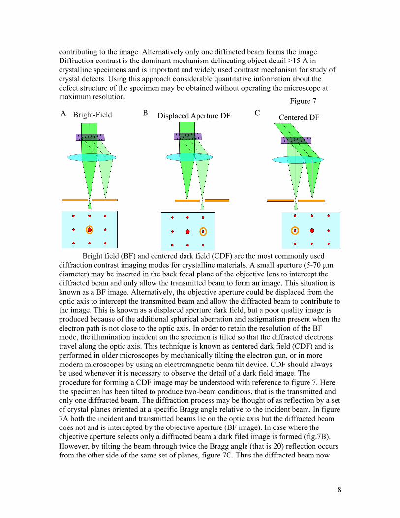
contributing to the image. Alternatively only one diffracted beam forms the image. Diffraction contrast is the dominant mechanism delineating object detail >15 Å in crystalline specimens and is important and widely used contrast mechanism for study of crystal defects. Using this approach considerable quantitative information about the defect structure of the specimen may be obtained without operating the microscope at maximum resolution.
Bright field (BF) and centered dark field (CDF) are the most commonly used diffraction contrast imaging modes for crystalline materials. A small aperture (5-70 µm diameter) may be inserted in the back focal plane of the objective lens to intercept the diffracted beam and only allow the transmitted beam to form an image. This situation is known as a BF image. Alternatively, the objective aperture could be displaced from the optic axis to intercept the transmitted beam and allow the diffracted beam to contribute to the image. This is known as a displaced aperture dark field, but a poor quality image is produced because of the additional spherical aberration and astigmatism present when the electron path is not close to the optic axis. In order to retain the resolution of the BF mode, the illumination incident on the specimen is tilted so that the diffracted electrons travel along the optic axis. This technique is known as centered dark field (CDF) and is performed in older microscopes by mechanically tilting the electron gun, or in more modern microscopes by using an electromagnetic beam tilt device. CDF should always be used whenever it is necessary to observe the detail of a dark field image. The procedure for forming a CDF image may be understood with reference to figure 7. Here the specimen has been tilted to produce two-beam conditions, that is the transmitted and only one diffracted beam. The diffraction process may be thought of as reflection by a set of crystal planes oriented at a specific Bragg angle relative to the incident beam. In figure 7A both the incident and transmitted beams lie on the optic axis but the diffracted beam does not and is intercepted by the objective aperture (BF image). In case where the objective aperture selects only a diffracted beam a dark filed image is formed (fig.7B). However, by tilting the beam through twice the Bragg angle (that is 2θ) reflection occurs from the other side of the same set of planes, figure 7C. Thus the diffracted beam now
Bright-Field Centered DFDisplaced Aperture DF
Figure 7 A B C

9
lies on the optic axis while the transmitted beam follows the original path of the diffracted beam and is stopped by the objective aperture. Thickness fringes
Due to diffraction from the periodical arrangements of atoms in crystalline materials the intensity of the transmitted electron beam oscillates with depth with a periodicity of ξg, which is known as the extinction distance. The transmitted intensity is zero for specimen thickness (n + 1/2) ξg, where n is an integer. Consequently the edge of a typical wedge-shaped crystalline foil exhibits dark fringes connecting regions of the same thickness 0.5ξg, 1.5ξg, 2.5ξg etc (Fig. 8). However, when absorption is allowed for, the fringes are damped with increasing thickness and disappear before the transmitted intensity is zero. This often occurs above ~ 5 fringes. Clear high-contrast images of crystal defects are generally obtained at thickness where the thickness fringes just damp out. The thickness fringes show opposite contrast in dark field. Under kinematical conditions these thickness fringes almost disappear. The extinction distance ξg depends on both the operative reflection and the deviation from the exact Bragg position. Thus the spacing of the extinction fringes in an electron microscope image change if the operative reflection is changed by tilting the specimen or if s varies from point to point in the specimen because of bending of the foil. PHASE CONTRAST
Contrast in TEM images can arise due to the differences in the phases of the electron waves scattered through a thin specimen. The mode we refer to as phase contrast imaging has been used primarily because the method is capable of resolving sub-unit-cell detail. Whereas conventional bright- and dark-field TEM studies usually utilize only the central electron beam or a single diffracted beam, the phase contrast method relies on interference among at least two beams and commonly many beams. The electrons leaving the bottom surface of a thin electron microscope specimen have small phase differences arising from scattering in the specimen. However, to convert these phase differences into intensity differences in the final image, it is necessary to introduce additional phase shifts using the spherical aberration and defocusing effects of the objective lens.
Phase contrast effects are important in direct lattice plane resolution, multi-beam lattice images, Moiré patterns, and point-to-point resolution tests. Phase contrast imaging is the basis for the co called high-resolution TEM (HRTEM).
Phase contrast carries very significant information about the studied materials since in addition to the diffracted beams, which provide information about the periodically ordered part of the crystals, the diffuse intensity between Bragg reflections
Figure 8

10
contributes to the image as well, providing information on non-periodical features and defects. For a structurally ordered crystal, the method produces an image that shows the periodicity of the crystal lattice and hence is sometimes called lattice imaging. Under ideal experimental conditions, an image that resembles the projected structure of the specimen may be obtained, in which case the technique is sometimes called structure imaging.
As with any other electron microscopic technique, HRTEM has its strengths -and its weaknesses. Although HRTEM can be used to image dislocations and antiphase domain boundaries, for example, conventional TEM methods are better suited for many studies of such defects, since HRTEM usually gives only projected fault vectors. The strength of HRTEM lies in its ability to resolve the detailed structures of complex planar faults, disordered structures, and interfaces that are not obtainable by diffraction contrast imaging methods as shown on figure 9, where one
unit-cell-wide defect in amphibole crystal is shown. An introduction to vacuum Electron microscopes cannot operate in air for a number of reasons. The penetration of electrons through air is typically no more than 1 meter, so after coming on meter from the gun, the whole beam would be lost to collisions of the electrons with the air molecules. It is also not possible to generate the high charge difference between the anode and cathode in the gun because air is not a perfect insulator. Finally, the beam on the specimen while in air would trap all sorts of rubbish (air is full of hydrocarbon molecules) on the specimen, crack them (removing hydrogen, oxygen, etc.) and thus leave a thick carbon contamination layer on the specimen. Each electron microscope therefore has a vacuum system. the degree of sophistication of the vacuum system depends on the requirements. Simple imaging of biological thin sections is much less demanding than cryo applications or small-probe analysis in materials science, and a thermionic gun can operate under much worse vacuum than a Field Emission Gun. The most basic vacuum system consists of a vessel connected to a pump that removes the air. The vacuum system of an electron microscope is considerably more complicated, containing a number of vessels, pumps, valves (to separate different vessels) and gauges (to measure vacuum pressures). From the bottom up we can distinguish four vessels in the vacuum system: • The buffer tank • The projection chamber • The column (specimen area) • The electron gun area
Figure 9

11
These are not pumped by single pump, because there is no pump available that handle the full range in vacuum from air pressure (as present after a vessel has been vented) to ultra-high vacuum (in specimen are or gun). The microscope can in essence be divided in two parts, separated by a very small aperture (200 micrometers), the differential pumping aperture, located between the projection chamber and the column.
The lower part basically consists of the projection chamber where we observe the image and where plate camera and TV cameras are located. This is pumped by an oil-diffusion pump. Behind the oil-diffusion pump is a rotary pump (the oil-diffusion pump cannot go from vacuum to air, it needs some other pump to back it up). Since the rotary (or pre-vacuum) pump is noisy, it is not running continuously but only when needed. In order to have continuous backing of the diffusion, there is a buffer tank in between them. The buffer tank is slowly filled by the oil-diffusion pump. When its pressure is becoming high, it is emptied by the rotary pump. The upper part consists of the specimen and gun areas, which are pumped by one or more ion-getter pumps. These pumps use no oil and are therefore clean. They also achieve higher vacuum than the oil-diffusion pump. The number of ion-getter pumps may range from one to four. Initial pumping of the column and gun on many systems is done by the rotary and oil-diffusion pumps, except for systems equipped with a turbo-molecular pump. In the latter case the oil-diffusion and rotary pumps never pump on the column and gun areas. Limitations of electron microscopy Sampling
The TEM studies very small volumes. The higher the resolution the smaller the analyzed volume becomes. The TEM is extreme in this respect. It is estimated by Williams and Carter (1996) that from the first implementation of TEM till 1996 a total volume of 0.6 mm3 has been analyzed by HRTEM. This emphasizes the need to study your sample on gradually decreasing scale and try to prepare TEM samples from truly representative material. In general light microscopy should precede electron microscopy and SEM must precede TEM studies. Drawing conclusions from a single observation or even single sample is dangerous and can lead to completely false interpretations. Dimensionality
TEM images are two-dimensional projections of 3D objects. We must be very cautious in interpreting shapes, and spatial relationships especially in the TEM. Also TEM data averages the whole examined volume and it is not a suitable method for surface analysis. This is true also for the SEM which caries information from a depth in the range of 1 to 2 µm below the surface. For true surface analysis surface methods need to be applied. Beam Damage
The high energy of the electron beam utilized in electron microscopy causes damage by ionization, radiolysis, and heating. In summary the electron beam can completely destroy the sample by amorphisizing or melting and even evaporating it.

12
Sample preparation The requirement for thin specimens containing no volatile components limits the
range of possible materials to be studied with TEM. Another aspect of sample preparation for TEM is that during the process of preparation modifications and alteration of the sample may take place, which need to be taken into account and artifacts need to be reliably identified in order to gain reliable information.
A TEM can be used in any branch of science and technology where it is desired to study the internal structure of specimens down to the atomic level. It must be possible to make the specimen stable and small enough (around 3 millimeters in diameter) to permit its introduction into the evacuated microscope column and thin enough to permit the transmission of electrons. Different thicknesses are required for different applications. For the ultimate high-resolution materials studies, the sample cannot be thicker than 20 nm or so; for bio-research, the film can be 300-500 nm thick.
Every branch of research has its own specific methods of preparing the specimen for electron microscopy.
In biology, for example, there may be first a chemical treatment to remove water and preserve the tissue as much as possible in its original state, followed by embedding in a hardening resin; after the resin has hardened, slices (sections) with an average thickness of 0.5 µm are cut with an instrument called an ultramicrotome equipped with a glass or diamond knife. The tiny sections thus obtained are placed on a specimen carrier - usually a 3 mm diameter specimen grid that has been coated with an amorphous carbon film about 10 nm thick.
In metallurgy, a 3 mm diameter disc of material (a thickness of approximately 0.3 mm) is chemically treated in such a way that in the center of the disc the material is fully etched away. Around this hole there will usually be areas that are sufficiently thin (approximately 100 nm) to permit electrons to pass through.
To study non-metal solid state materials such as minerals, semiconductors, ceramics etc. the use of a focused ion beam to mill and thin a section from a bulk specimen is the most efficient way of sample preparation. For this purpose either ion mill or Focused Ion Beam (FIB) instruments are utilized.
FURTHER READING D B. Williams and C. Barry Carter. Transmission electron microscopy: a textbook for
materials science. New York, Spinger, 2009. L. Reimer, H. Kohl Transmission electron microscopy: physics of image formation New
York, NY: Springer, 2008 B. Fultz, J. Howe Transmission electron microscopy and diffractometry of materials.
Berlin; New York: Springer, 2008 J Bozzola; L D Russell. Electron microscopy: principles and techniques for biologists.
Boston, Jones and Bartlett, 2006.


![Leica M-Lenses - overgaard.dk · Leica M Lenses [3] Contents Contents Introduction 1 The Soul of Leica M-Lenses 4 Core Technologies 12 MTF Analysis: those shapely curves 15 Color](https://img.pdfslide.us/doc/110x75/5d5adec288c9936f5d8b6532/leica-m-lenses-leica-m-lenses-3-contents-contents-introduction-1-the-soul.jpg)
![Leica M-Lenses: Their Soul and Secrets. - Thorsten · PDF fileLeica M Lenses [1] Introduction Secrets revealed It is well known that Leica M lenses, in spite of their compact design,](https://img.pdfslide.us/doc/110x75/5a79135b7f8b9a523d8cb853/leica-m-lenses-their-soul-and-secrets-thorsten-m-lenses-1-introduction.jpg)