Embed Size (px)
Citation preview
ELCTEC-131 Advanced Digital Electronics MATC Richard Lokken Adapted for the DE1 board
Experiment 7 Introduction to Quartus II (Tutorial)
Objectives Upon completion of this laboratory exercise, you should be able to: • Create a project in Quartus II. • Use the Quartus Block Editor to enter a graphical design in Quartus II. • Compile and simulate the design. • Program an Altera CPLD with the design. • Test the design on a CPLD test board to determine its truth table. Lab Reference Equipment Required Dueck, Robert K., Digital Design with CPLD Applications and VHDL, 2/e
Chapter 4: Introduction to PLDs and Quartus II 4.6 Quartus II Design Flow and Graphical User Interface 4.7 Creating a Quartus II Project and Block Diagram File 4.8 Compiling and Simulating a Design in Quartus II 4.9 Transferring a Design to a Target CPLD CPLD Trainer:
Cyclone II FPGA Starter Development Kit Quartus II Web Edition software
EXPERIMENTAL NOTES
This lab will follow the tutorial steps laid out in Sections 4.6–4.9 in Chapter 4 of Digital Design with CPLD Applications and VHDL, 2/e. This example creates a project in Quartus II, enters a design file for a majority vote circuit, and programs an Altera CPLD with the design. PROCEDURE Creating a Quartus II Project and Block Diagram File
To create a new Block Diagram File, select New from the File menu. From the dialog box, shown in Figure 7.1, choose the Device Design Files tab and select Block Diagram/Schematic File. The Quartus II Block Editor will open, as shown in Figure 7.2.

ELCTEC-131 Advanced Digital Electronics MATC Richard Lokken Adapted for the DE1 board
Figure 7.1 New File Dialog Box (Block Diagram File)
Figure 7.2 Block Diagram File (Blank)

ELCTEC-131 Advanced Digital Electronics MATC Richard Lokken Adapted for the DE1 board
Before entering any design information, we will create a new project, with the new Block Diagram File as the top-level file in a design hierarchy.
To create the new project, first save the blank Block Diagram File, using the Save As dialog, shown in Figure 7.3. Change the file name to majority_vote.bdf and save the file in the folder drive:\qdesigns\labs\lab04\majority\. Make sure the box labeled Create new project based on this file is checked. The dialog box in Figure 7.4 will appear, asking you to confirm your choice.
Click Yes. This box should be checked.
Figure 7.3 Save as Dialog Box
Figure 7.4 New Project Query

ELCTEC-131 Advanced Digital Electronics MATC Richard Lokken Adapted for the DE1 board
After saving your file, the New Project Wizard will automatically appear. The New Project Wizard is a series of setup screens that asks the user for information about a project. Initially, there is an introductory screen, shown in Figure 7.5. The next screen, in Figure 7.6, asks for information about the directory the project will use, project name, and name of the top-level design entity. A directory name should be unique for each project and can be created by typing it in or selecting it from an existing directory list. By default, the screen in Figure 7.6 contains the directory where the new Block Diagram File was stored and its file name. (Figure 7.6 shows the file path for the example shown in Chapter 4 of Digital Design with CPLD Applications and VHDL, 2/e.) For most cases, simply accept the default names and click Next.
Figure 7.5 New Project Wizard (Intro)

ELCTEC-131 Advanced Digital Electronics MATC Richard Lokken Adapted for the DE1 board
Figure 7.6
New Project Wizard (Directory, Entity) The next screen, in Figure 7.7, shows the files currently included in the project and asks if any more should be added. Click Next. The screen in Figure 7.8 allows the user to select various third-party software tools as plug-ins to the Quartus II software. We will not be using this feature, so click Next to see the next screen.

ELCTEC-131 Advanced Digital Electronics MATC Richard Lokken Adapted for the DE1 board
Figure 7.7 New Project Wizard (Files)

ELCTEC-131 Advanced Digital Electronics MATC Richard Lokken Adapted for the DE1 board
Figure 7.8 New Project Wizard (Device Family and Target Device)
The screen in Figures 7.8 selects the device family (CyloneII) and target device (EP2C20F484C7) for the project. Click Next in each screen after making these selections.

ELCTEC-131 Advanced Digital Electronics MATC Richard Lokken Adapted for the DE1 board
Figure 7.9 New Project Wizard (EDA Tool Settings)
We will not be using of these tools, click Next.

ELCTEC-131 Advanced Digital Electronics MATC Richard Lokken Adapted for the DE1 board
Figure 7.10 New Project Wizard (Summary Screen)
The final screen, shown in Figure 7.10 is a summary of project settings provided by the user. Click Finish to exit the wizard. The wizard can be exited at any point if all the relevant information has been entered. Project settings can be altered at any time via the Settings dialog box, accessible from the Assignments menu. Entering Components
The first step in entering the majority vote circuit in the Quartus II Block Editor is to lay out and align the required components. We require three 2-input AND gates, a 3-input OR gate, three input pins, and one output pin. These basic components are referred to as primitives. Let us start by entering three copies of the AND gate primitive, called and2.

ELCTEC-131 Advanced Digital Electronics MATC Richard Lokken Adapted for the DE1 board
Open the Edit menu, shown in Figure 7.12, and select Insert Symbol, or simply
double-click on the Block Editor desktop. In the Symbol dialog box (Figure 7.13) type and2 in the box labeled Name. The and2 symbol appears in the desktop area on the right. Since we want to enter three instances of the symbol, check the box that is labeled Repeat-insert mode. Click OK.
Click on the desktop in the Block Editor window to place an instance of the and2
component. Don’t worry about its exact placement for the moment. Click two more times to place two more gates, and then use the ESC key to exit the insert-repeat mode.
Figure 7.12 Edit Menu (Insert Symbol)

ELCTEC-131 Advanced Digital Electronics MATC Richard Lokken Adapted for the DE1 board
Figure 7.13 Symbol Dialog Box (and2)
Enter the remaining components by following the Insert Symbol procedure outlined above. The primitives are called or3, input, and output. The insert-repeat mode is not necessary for the or3 and output components, as there is only one of each. When all components are entered we can align them, as in Figure 7.14 by highlighting, then dragging each one to a desired location.

ELCTEC-131 Advanced Digital Electronics MATC Richard Lokken Adapted for the DE1 board
Figure 7.14 Aligned Components
Connecting Components
To connect components, click over one end of one component and drag a line to one end of a second component, as shown in Figure 7.15. When you hover over a line end, the cursor changes from an arrow to a crosshair with a right-angle symbol. When you drag the line, a horizontal and a vertical grid helps you align connections properly. Smart cursor becomes a line tool when hovering over connector point.
Figure 7.15 Dragging a Line to Connect Components
A line will automatically make a connection to a perpendicular line, as shown in Figure 7.16.
A line can have one 90��bend, as at the inputs of the AND gates. If a line requires two bends, such as shown at the OR inputs in Figure 7.17, you must draw two separate lines.

ELCTEC-131 Advanced Digital Electronics MATC Richard Lokken Adapted for the DE1 board
Figure 7.16 Making a 90 Bend and a Connection
Figure 7.17 Making Two 90 �Bends

ELCTEC-131 Advanced Digital Electronics MATC Richard Lokken Adapted for the DE1 board
Assigning Pin Names
Before a design can be compiled, its inputs and outputs must be assigned names. Figure 7.18 shows the naming procedure. Pins a and b have already been assigned names. Double-click the pin name (not the pin symbol) to highlight the name. Type in the new name.
If there are several pins that are spaced one above the other, such as a, b, and c in
Figure 7.18, you can highlight the top pin name, as described above, then highlight successive pin names by using the Enter key.
Figure 7.18 Assigning Pin Names
Compiling and Simulating a Design in Quartus II
To start the compilation process, click the Start Compilation button on the Quartus II toolbar, as shown in Figure 7.19.
Start compilation
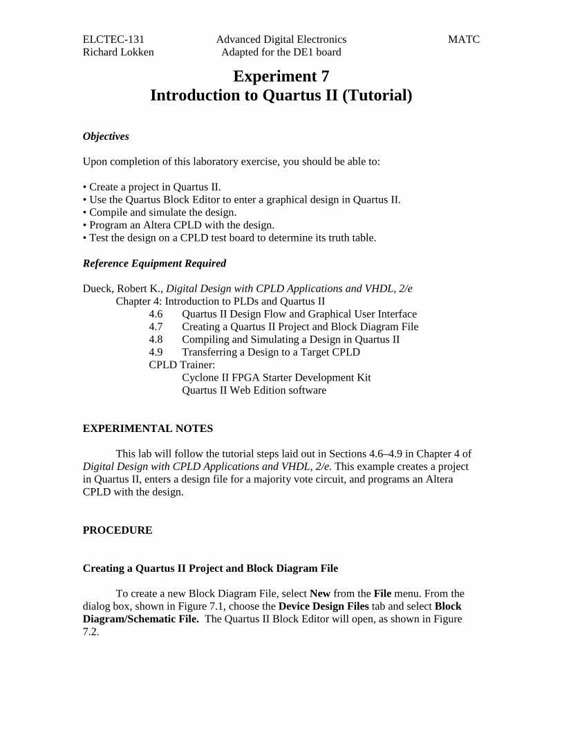
Figure 7.19 Start Compilation (Toolbar Button) When compilation is complete, Quartus II displays a Compilation Report, shown in Figure 7.20.
ELCTEC-131 Advanced Digital Electronics MATC Richard Lokken Adapted for the DE1 board
Figure 7.20 Compilation Report Window Simulation
Before we create a simulation for the majority vote circuit of our tutorial example, we should write a set of simulation criteria for the circuit. The circuit must generate a HIGH output when a majority of inputs is HIGH. Since we have three inputs, this means two or more inputs must be HIGH. The most thorough and systematic way to test the circuit is to apply all possible input combinations to the circuit in an ascending binary sequence, in other words, to take its truth table.
We can summarize the criteria, as follows.
Simulation Criteria
• Apply all possible inputs in an ascending binary sequence.
• For any input combination having two or more HIGH inputs (011, 101, 110, 111), the output must be HIGH.
• For any other input combination (000, 001, 010, 100), the output must be LOW.
A simulation is based on a Vector Waveform File (vwf), which contains
simulation input and output values in the form of graphical waveforms. To create a new vwf, select New from the File menu or click the appropriate toolbar button. From the box in Figure 7.21, click the Other Files tab and select Vector Waveform File.

ELCTEC-131 Advanced Digital Electronics MATC Richard Lokken Adapted for the DE1 board
The default window of the Quartus II Waveform Editor will appear, as shown in Figure 7.22.
Figure 7.21 New File Dialog Box (Vector Waveform File)

ELCTEC-131 Advanced Digital Electronics MATC Richard Lokken Adapted for the DE1 board
Figure 7.22 Waveform Editor (Default)
To add waveforms to the window, we can use the Node Finder. Start the Node Finder by clicking on the Node Finder toolbar button or selecting Utility Windows, Node Finder from the View menu. The default window opens, as shown in Figure 7.23. Click Start to display a list of nodes, or signal points, for the project. The window in Figure 7.24 shows a list of available nodes for the project. We are only interested in a, b, c, and y; the others represent logic levels internal to the circuit.
Select Design Entry (all Names)
Figure 7.23 Node Finder (Default)

ELCTEC-131 Advanced Digital Electronics MATC Richard Lokken Adapted for the DE1 board
Figure 7.24 Node Finder (Nodes Selected)
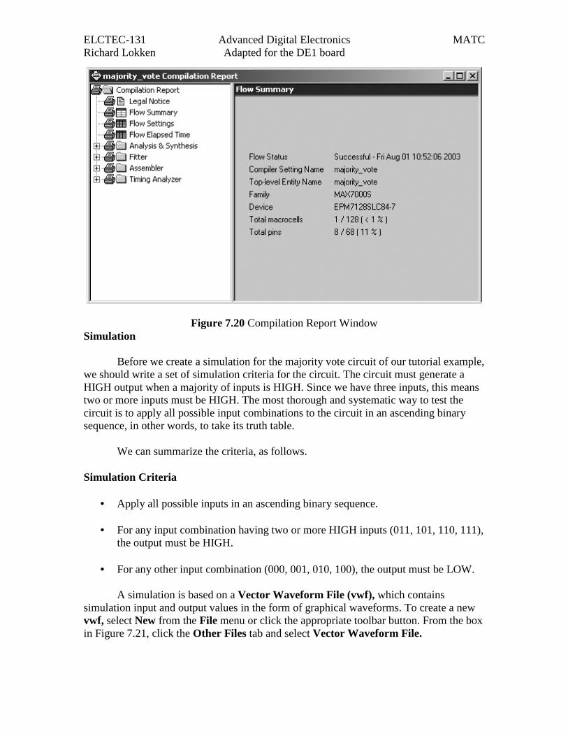
Add the required nodes to the Vector Waveform File by dragging them from the Node Finder to the Waveform Editor window. Do this by clicking on a waveform to highlight it, then drag and drop to place it in the Waveform Editor, as shown in Figure 7.25.
ELCTEC-131 Advanced Digital Electronics MATC Richard Lokken Adapted for the DE1 board
Drag node from here to here
Figure 7.25 Dragging from Node Finder to Vector Waveform File
Once the waveforms have been added to the Waveform Editor, close the Node Finder window and save the Vector Waveform File, using the Save As dialog box in Figure 7.26. Make sure that the box labeled Add file to current project is checked. (This step could be done earlier, such as immediately after creating a new Vector Waveform File.)

ELCTEC-131 Advanced Digital Electronics MATC Richard Lokken Adapted for the DE1 board
This box should be checked
Figure 7.26 Save as Dialog Box (Adding vwf to Project)
Once we have entered the input and output nodes, we must determine the length of time our simulation should run. The default time is 100 ns. The target CPLD has a delay time from input to output of about 7 ns. (This is indicated by the –7 at the end of its part number.) If we changed our inputs every 10 ns, we would have sufficient room in the simulation to display ten input changes, which is enough to fit in the eight changes we need, plus a little more. However, due to the input-to-output delay in the target device, the output would not change until it is nearly time for a new input change. This delayed output would produce an offset waveform that would be confusing to read. In this case, we would be better off with a simulation time that is long compared to the input-to-output delay of the target device.
To change the end time of the simulation, select End Time from the Edit menu,
shown in Figure 7.27. In the End Time dialog box, shown in Figure 7.28, change the unit from ns to us (microseconds). This is an easy change that gives a simulation time that is long compared to device delay time.

ELCTEC-131 Advanced Digital Electronics MATC Richard Lokken Adapted for the DE1 board
Figure 7.27 Edit Menu (End Time)
Figure 7.28 End Time Dialog Box To see the entire waveform file, select Fit in Window from the View menu.
Alternatively, you can customize the Waveform Editor toolbar to have buttons for the zoom tools Zoom In, Zoom Out, and Fit in Window, as shown in Figure 7.29. (The buttons can be found under Tools, Toolbars, Commands, Zoom in Quartus II. Drag and drop the buttons onto the Waveform Editor toolbar.)

ELCTEC-131 Advanced Digital Electronics MATC Richard Lokken Adapted for the DE1 board
We could enter waveforms on a, b, and c individually to create an increasing 3-bit binary sequence, but it is easier and more accurate to group these waveforms together and apply the sequence to the whole group. Figure 7.30 shows a highlighted group of waveforms in the Quartus II Waveform Editor. To highlight a group, click on the top waveform (a), then drag the cursor to the last waveform of the group (c). Right-click on the highlighted group of waveforms and select Group . . . from the pop-up menu of Figure 7.31. Type the group name (Inputs) in the dialog box of Figure 7.32. Select the radix (i.e., the number system base) as Binary. Click OK. The grouped waveforms appear as shown in Figure 7.33.
Zoom in Zoom out Fit in window
Figure 7.29 Waveform EditorToolbar (Customized to show ZoomTools)

ELCTEC-131 Advanced Digital Electronics MATC Richard Lokken Adapted for the DE1 board
Figure 7.30 Highlighting a Group of Waveforms
Figure 7.31 Pop-up Menu (Group)

ELCTEC-131 Advanced Digital Electronics MATC Richard Lokken Adapted for the DE1 board
Figure 7.32 Group Name and Radix
Figure 7.33 Grouped Waveforms
Click on the waveform group (Inputs) to highlight it and apply an increasing binary count to the group by clicking the Count Value toolbar button, shown in Figure 7.34, or by selecting Value, Count Value from the Edit menu. In the Counting tab of the Count Value dialog box, shown in Figure 7.35, select Radix: Binary; Start value: 000; Increment by: 1; and Count type: Binary. End value is calculated from the other parameters of the simulation.

ELCTEC-131 Advanced Digital Electronics MATC Richard Lokken Adapted for the DE1 board
Figure 7.34 Waveform
Figure 7.35 Count Waveform Dialog Counting

ELCTEC-131 Advanced Digital Electronics MATC Richard Lokken Adapted for the DE1 board
Figure 7.36 Count Waveform Dialog (Timing)
In the Timing tab, shown in Figure 7.36, select Start time: 0 ps; End time: 100 us; Count every: 10.24 us; and Multiplied by: 1. The count interval of 10.24 �s is selected to match the spacing of the Waveform Editor timing grid. Click OK to accept the values. The count waveforms will appear as shown in Figure 7.37. The binary value on Inputs corresponds to the combined HIGH and LOW values on inputs a, b, and c.
Figure 7.37 Count Waveform on Inputs
ELCTEC-131 Advanced Digital Electronics MATC Richard Lokken Adapted for the DE1 board
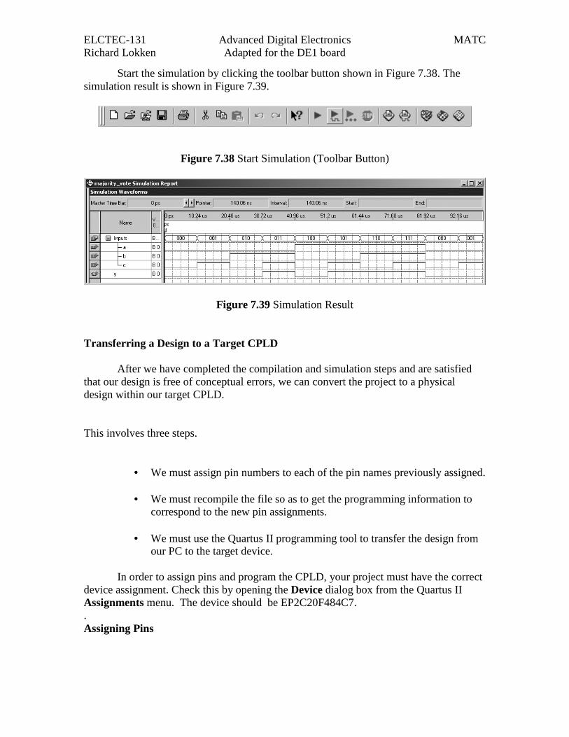
Start the simulation by clicking the toolbar button shown in Figure 7.38. The simulation result is shown in Figure 7.39.
Figure 7.38 Start Simulation (Toolbar Button)
Figure 7.39 Simulation Result Transferring a Design to a Target CPLD
After we have completed the compilation and simulation steps and are satisfied that our design is free of conceptual errors, we can convert the project to a physical design within our target CPLD.
This involves three steps.
• We must assign pin numbers to each of the pin names previously assigned.
• We must recompile the file so as to get the programming information to correspond to the new pin assignments.
• We must use the Quartus II programming tool to transfer the design from
our PC to the target device. In order to assign pins and program the CPLD, your project must have the correct
device assignment. Check this by opening the Device dialog box from the Quartus II Assignments menu. The device should be EP2C20F484C7. . Assigning Pins

ELCTEC-131 Advanced Digital Electronics MATC Richard Lokken Adapted for the DE1 board
We can assign pins either from a dialog box dedicated to this task or from the Quartus II Assignment Editor. The procedure for using the Assignment Editor is outlined below. For information on using the Assign Pins dialog box instead, see the relevant part of Section 4.9 in Digital Design with CPLD Applications and VHDL, 2/e. Note
We will use the following pin assignments for the majority vote example:
Pin Name
Pin Number
On Board
A PIN_L22 SW(0) B PIN_L21 SW(1) C PIN_M22 SW(2) Y PIN_R20 LEDR(0)
Using the Quartus II Assignment Editor
Open the Pins from the Assignments menu, as shown in Figure 7.40.

ELCTEC-131 Advanced Digital Electronics MATC Richard Lokken Adapted for the DE1 board
Figure 7.40 Assignments Menu (Pins)

ELCTEC-131 Advanced Digital Electronics MATC Richard Lokken Adapted for the DE1 board
Figure 7.41 Assignment Editor (Pin Assignments)
Under the Name column, type a pin name. Select the name from the drop-down
box, as shown in Figure 7.43. When you have made all assignments, close the pin planner box. Recompile the project.

ELCTEC-131 Advanced Digital Electronics MATC Richard Lokken Adapted for the DE1 board
Figure 7.43 Adding Pin Numbers from a Drop-Down Menu
Once the pins have been assigned, they will appear in the Block Diagram File, as shown in Figure 7.44.
Figure 7.44 Majority Vote Circuit, showing Pin Numbers Programming CPLDs on the Altera UP-1 or UP-2 Circuit Board
The CPLDs on the Altera DE1 circuit board is programmed via the programming software in Quartus II and a USB cable called the USB Byte Blaster.

ELCTEC-131 Advanced Digital Electronics MATC Richard Lokken Adapted for the DE1 board
Quartus II Programmer To program a device on the Altera DE1 board set the run/prog switch to run. Ensure the board is turned on and connected to the USB port on your computer.
Start the Quartus II Programmer, either with the toolbar button shown in Figure 7.45 or by selecting Programmer from the Tools menu (Figure 7.46). The programmer dialog box (Figure 7.47) will open, showing the programming file for the top-level file of the open project.
Figure 7.45 Programmer Toolbar Button
Figure 7.46 Tools Menu (Programmer) If you have never programmed a CPLD with your particular version of Quartus II,
you will need to set up the programming hardware before proceeding. To set up the USB Byteblaster see the tutorial on byteblaster setup on blackboard.
Click the Hardware button at the top left corner of the Programmer dialog box. The Hardware Setup dialog box, shown in Figure 7.47, will open. Click the Add Hardware button. In the Add Hardware dialog in Figure 7.48, select Hardware type: USB Blaster (USB-0). Click OK to accept the choices and close the box. In the Hardware Setup dialog, highlight USB Blaster (USB-0) in the Available hardware items box by clicking the item, then click Select Hardware. Click Close to return to the Programmer dialog.

ELCTEC-131 Advanced Digital Electronics MATC Richard Lokken Adapted for the DE1 board
Figure 7.47 Programmer Dialog Box
Figure 7.48 Hardware Setup Dialog box

ELCTEC-131 Advanced Digital Electronics MATC Richard Lokken Adapted for the DE1 board
Figure 7.45 shows the programmer dialog box, now with the programming hardware selected. In order to program the CPLD, highlight the required programming file by clicking it, then select the checkbox for Program/Configure.
Start programming the CPLD by clicking the Start button, shown in Figure 7.45.
The majority vote circuit can be tested on a CPLD board, such as the Altera DE1 board or equivalent. When two of the threeswitches are HIGH, there should be a HIGH at the CPLD output. The toggle switches are low when in the down position (at the boards edge) and high when in the up position (toward the LEDs)