Embed Size (px)
Citation preview

Introduction to Programmable Logic Devices
(Class 7.2 – 2/28/2013)
CSE 2441 – Introduction to Digital Logic
Spring 2013
Instructor – Bill Carroll, Professor of CSE

Today’s Topics
• Complexity issues
– Implementation
– Design
• Programmable logic devices
– Simple Programmable Logic Devices (SPLDs) • Programmable Logic Arrays (PLAs)
• Programmable Array Logic (PALs)
– Programmable Read Only Memory (PROM)
– Complex Programmable Logic Devices (CPLDs)
– Field Programmable Logic Devices (FPGAs)

Issues In Digital Circuit Implementation and Design
• Gates per integrated circuit
• Pin limitations
• Wiring complexity
• Speed
• Heat dissipation
• Design time
• More-complex functionality
• Testability
• Cost

Advances In Digital Circuit Implementation and Design
• Higher levels of integration
• Larger packages
• More pins per package
• New and improved technologies
• Multilayer printed circuit boards
• Application Specific ICs (ASICS)
• Programmable logic
• CAD tools
• Automated testing

Basic Programmable Logic Array Organization

Two-Level AND-OR Arrays
abc + bc
a
b
c
a
b
c
abc bc
(b)
x
x
x
x
x
xx
Realization of f(a,b,c) = abc’ + b’c
Figure 5.5

Multiple Functions Realized by an AND-OR Array
Figure 5.6
a
b
c
ab
f1(a, b, c) = ab + c
f2(a, b, c) = ab + bc
bcc
x
x
x
x
x
x
x
x
x
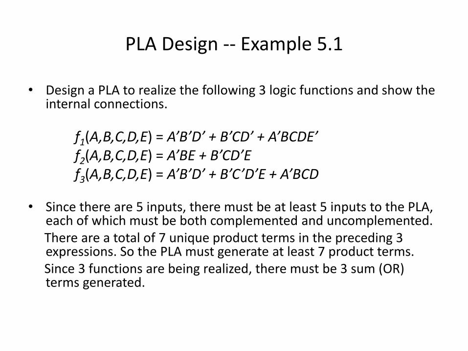
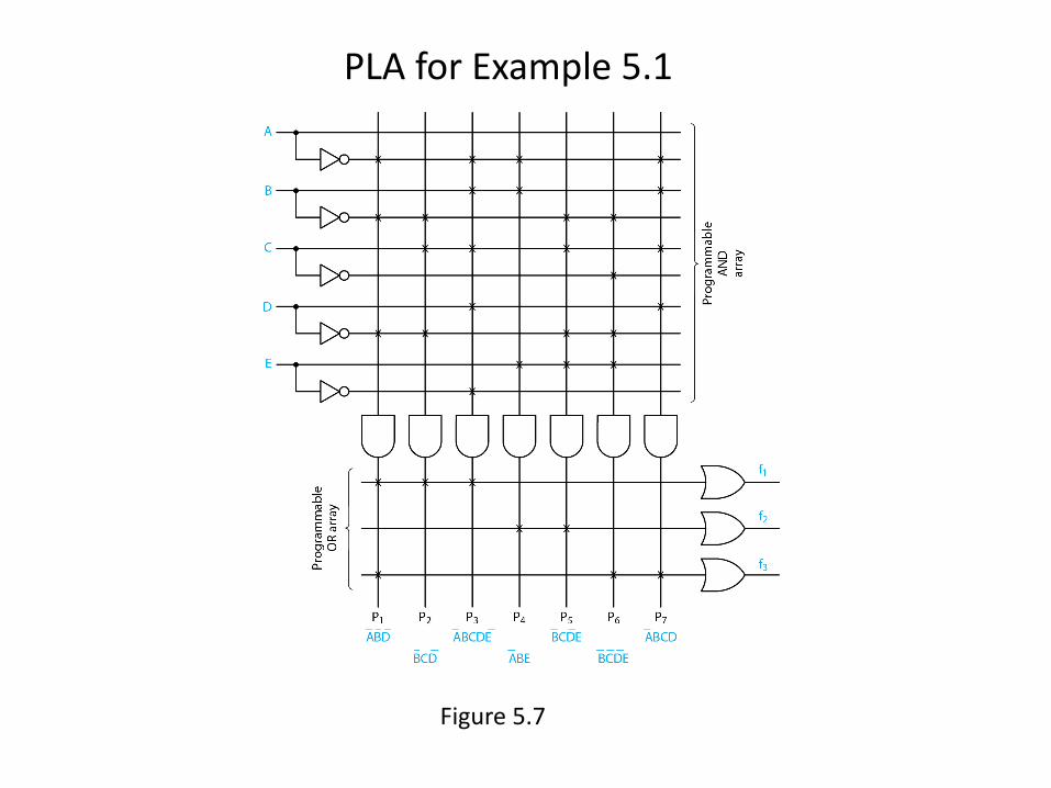
PLA Design -- Example 5.1
• Design a PLA to realize the following 3 logic functions and show the internal connections.
f1(A,B,C,D,E) = A’B’D’ + B’CD’ + A’BCDE’ f2(A,B,C,D,E) = A’BE + B’CD’E f3(A,B,C,D,E) = A’B’D’ + B’C’D’E + A’BCD
• Since there are 5 inputs, there must be at least 5 inputs to the PLA, each of which must be both complemented and uncomplemented.
There are a total of 7 unique product terms in the preceding 3 expressions. So the PLA must generate at least 7 product terms.
Since 3 functions are being realized, there must be 3 sum (OR) terms generated.

Example 5.1 (continued)
The PLA organization is shown in Fig. 5.7.
Table 5.1 shows the connections that must be made in the AND and OR arrays. In the table, the product term numbers correspond to the AND gate numbers in Fig. 5.7, each connected to one vertical product line, on which a product term is generated.
In the AND array portion of the table
- a 0 indicates that the complement of the variable is connected to the product line
- a 1 indicates the the uncomplemented input is connected to the product line
- an indicates that neither is connected to the product line
For the OR array, a 1 indicates a connection and a 0 indicates no connection.
PLA for Example 5.1
Figure 5.7
Table 5.1 -- PLA Table for Example 5.1
AND Array OR Array Inputs Outputs Product Term ABCDE f1f2f3
1 2 3 4 5 6 7
000 010 01110 01 1 0101 0001 0111
101 100 100 010 010 001 001
A’B’D’ B’CD’ A’BCDE’ A’BE B’CD’E B’C’D’E A’BCD

Basic Programmable Logic Array Organization

Output Polarity Options
Figure 5.11
Product
terms
Inputs
Il
Ik
Pl P
m
+V
Fuse
Active high (H)
Active low (L)
Active high
Active low
Complementaryoutputs (C)
Programmable
polarity (P)
.
(a)
.
.
. ..

Output Polarity Options(continued)
Figure 5.11
(b)
Si
Oi = S
i Oi = S
i
(c)
Si
x

Implementation of SOP and POS Forms
Figure 5.12
A
B
C
AB AC AB AC
f1
f2
*
*
*
*
*
*
*
*
**
**
*

Bidirectional Pins and Feedback Lines
• A bidirectional pin is driven by a three-state driver, whose control line is connected to one of the product terms.
• When the control line is 1, the driver is said to be enabled and functions as a short circuit, as shown in Fig. 5.13b. In this case the sum term is driven onto the pin, which therefore functions as an output. This value is fed back to the AND array, where it can be used to form product terms.
• When the driver control line is 0, the driver is disabled and functions as an open circuit, as shown in Fig. 5.13c. This disconnects the sum term from the pin, which, through the feedback line, now becomes an input to the AND array.

Bidirectional Pins
Figure 5.13
PnP
1
(a)
Pn + 1
Feedback
Three-statedriver
IOm
I1
Ik
.
Sm
..
.
..
...

Bidirectional Pins(continued)
Figure 5.13
(c)
Sm
Feedback = Sm
IOm
(output)
Sm
Feedback = IOm
IOm
(input)
(b)

Two-bit ripple-carry adder Example 5.3
• Implement a 2-bit ripple-carry adder, as shown in Fig. 5.14a, using a programmable logic array having 4 dedicated input pins, 3 dedicated output pins, and 3 bidirectional pins.
The standard logic equations for one state, i, of an n-bit full-adder are the following:
Si = AiBiCi-1 + AiB’iC’i-1 + A’iBiC’i-1 + A’iB’iCi-1
Ci = AiBi + AiCi-1 + BiCi-1
where Ai and Bi are the data inputs and Ci-1 the carry input to stage i, Si is its sum output and Ci the carry output. For a ripple-carry adder, the carry-out of one stage is connected to the carry input of the next stage, as shown in Fig. 5.14a.
Example 5.3(continued)
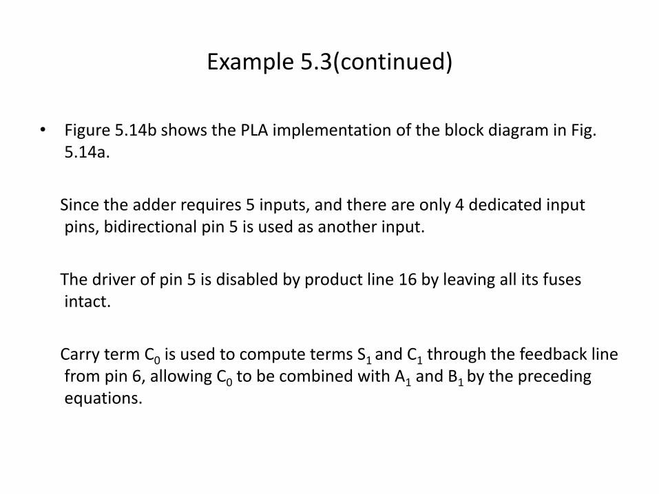
• Figure 5.14b shows the PLA implementation of the block diagram in Fig. 5.14a.
Since the adder requires 5 inputs, and there are only 4 dedicated input pins, bidirectional pin 5 is used as another input.
The driver of pin 5 is disabled by product line 16 by leaving all its fuses intact.
Carry term C0 is used to compute terms S1 and C1 through the feedback line from pin 6, allowing C0 to be combined with A1 and B1 by the preceding equations.

Two-bit Ripple-carry Adder – Example 5.3
Figure 5.14

Programmable Read-only Memory
• A PROM comprises a fixed AND array and a programmable OR array, as illustrated in Fig. 5.21.
The AND array generates all 2n possible minterm products of its n inputs and therefore often referred to as an n-to-2n decoder.
The OR array allows any combination of product terms to be included in each sum term. The canonical sum of products form of any function can be realized directly from its truth table or minterm list.
• Figure 5.22 illustrates the organization of most typical commercial PROMs.

Programmable Read-only Memory (PROM)
Figure 5.21
I0
I1
I2
m0
m1
m2 m
3m
4 m5 m
6m
7
Ok
O1
O2
Fixed
AND
array
Minterms
Programmable
OR array.
.
.

General Configuration of a Commercial PROM
Figure 5.22
A0
A1
AN-1
CE
P0 P
1 P2N-1
OMO
1 O2
ANDarray
Outputs
Productterms
Outputdrivers
Chip enable
.
Inputs
.
ORarray
.
.
..
.. .

Realizing Logic Functions with PROMs
• Each output of a PROM is capable of realizing any arbitrary switching function by connecting that output to the minterms of the function.
To realize a given switching function with a PROM, first express the function in canonical SOP form or else derive the truth table of the function.
Then, each of the minterms of the function is connected to the desired OR term to produce the canonical SOP form.
• It should be noted that the use of a commercially available PROM would be very inefficient when only a small number of minterms is needed, unless minimizing chip count is the primary goal.

PROM Realization -- Example 5.6
Realize the following 3 switching functions with a 3-input, 3-output PROM.
f1(A, B, C) = AB + B’C
f2(A, B, C) = (A + B’ + C)(A’ + B)
f3(A, B, C) = A + BC
First, convert each function to canonical SOP form.
f1(A, B, C) = ABC’ + ABC + A’B’C + AB’C
= m(1, 5, 6, 7)
f2(A, B, C) = (A + B’ + C)(A’ + B + C’)(A’ + B + C)
= M(2, 4, 5) = ∑m(0, 1, 3, 6, 7)
f3(A, B, C) = AB’C’ + ABC’ + AB’C + ABC + A’BC
= m(3, 4, 5, 6, 7)

PROM Realization for Example 5.6
Figure 5.23
Lookup Tables (LUT)
• A common application of PROMs is the lookup table, in which a function is stored in tabular form with its arguments used as an index into the table to retrieve the value of the function for those arguments.
• Since truth tables can be readily realized by PROMs, lookup tables are implemented by writing them in truth table format and then realizing the truth table with a PROM.

Programmable Array Logic (PAL)

Example 5.10 – PAL Design Example
Realize the following functions with a PAL
fα(A,B,C,D) = A’B’D’ + B’CD’ + A’BCD
fβ(A,B,C,D) = A’B + B’CD’
fγ(A,B,C,D) = A’B’D’ + B’C’D’ + A’BCD

Example 5.10 -- PAL Realization
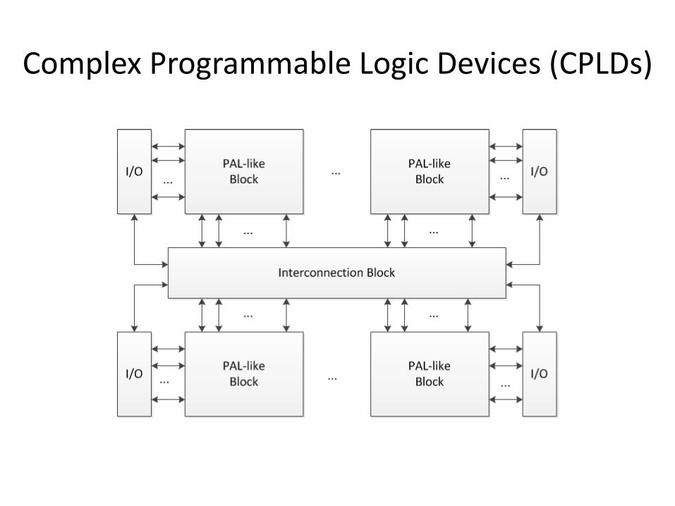
Complex Programmable Logic Devices (CPLDs)

Summary of Programmable Logic Devices
• PLA – AND array and OR array are programmable
• PAL – AND array programmable, OR array fixed
• PROM – AND array fixed, OR programmable
• CPLD – programmable array of PALs
• FPGA – programmable array of logic elements

Cyclone II FPGA*
*From Cyclone II Device Family Data Sheet
LAB – Logic Array Block, PLL – Phase Locked Loop, IOEs – I/O Elements

Cyclone II FPGA Family Features*
*From Cyclone II Device Family Data Sheet

Cyclone II Package Options*
*From Cyclone II Device Family Data Sheet
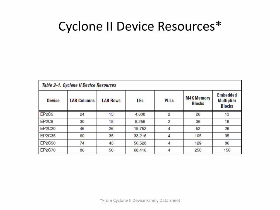
Cyclone II Device Resources*
*From Cyclone II Device Family Data Sheet

Cyclone II Logic Element Architecture*
*From Cyclone II Device Family Data Sheet
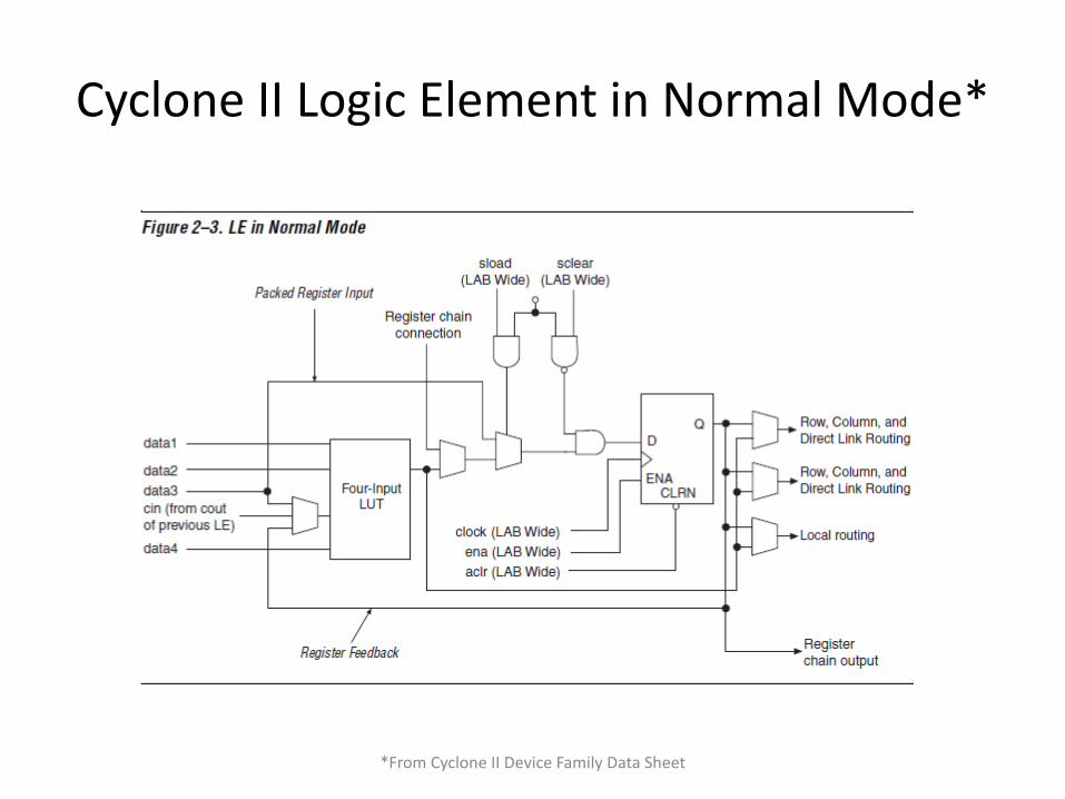
Cyclone II Logic Element in Normal Mode*
*From Cyclone II Device Family Data Sheet
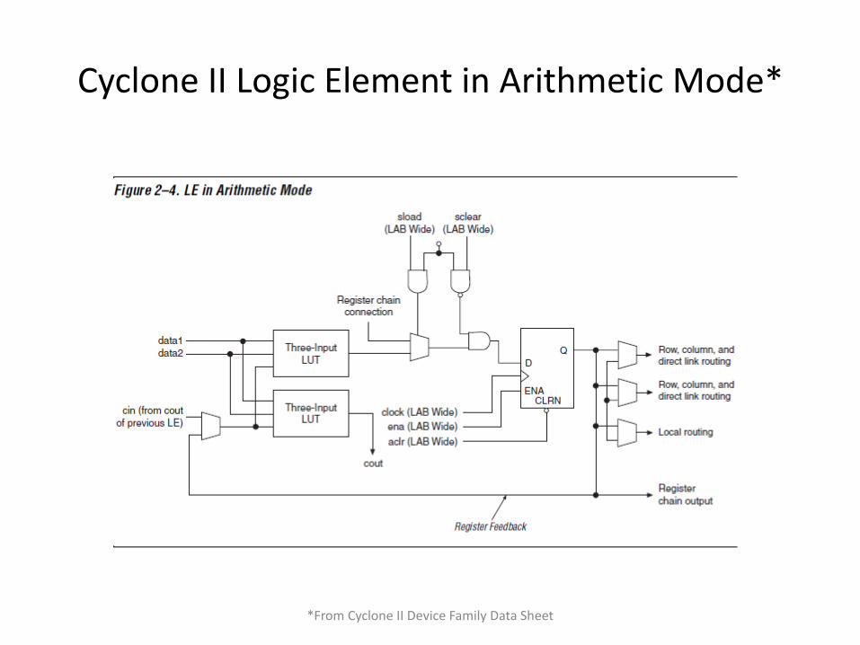
Cyclone II Logic Element in Arithmetic Mode*
*From Cyclone II Device Family Data Sheet