Embed Size (px)
Citation preview
Introduction to Power Semiconductor Devices
Zheng Yang(ERF 3017, email: [email protected])
ECE442 Power Semiconductor Devices and Integrated Circuits
2
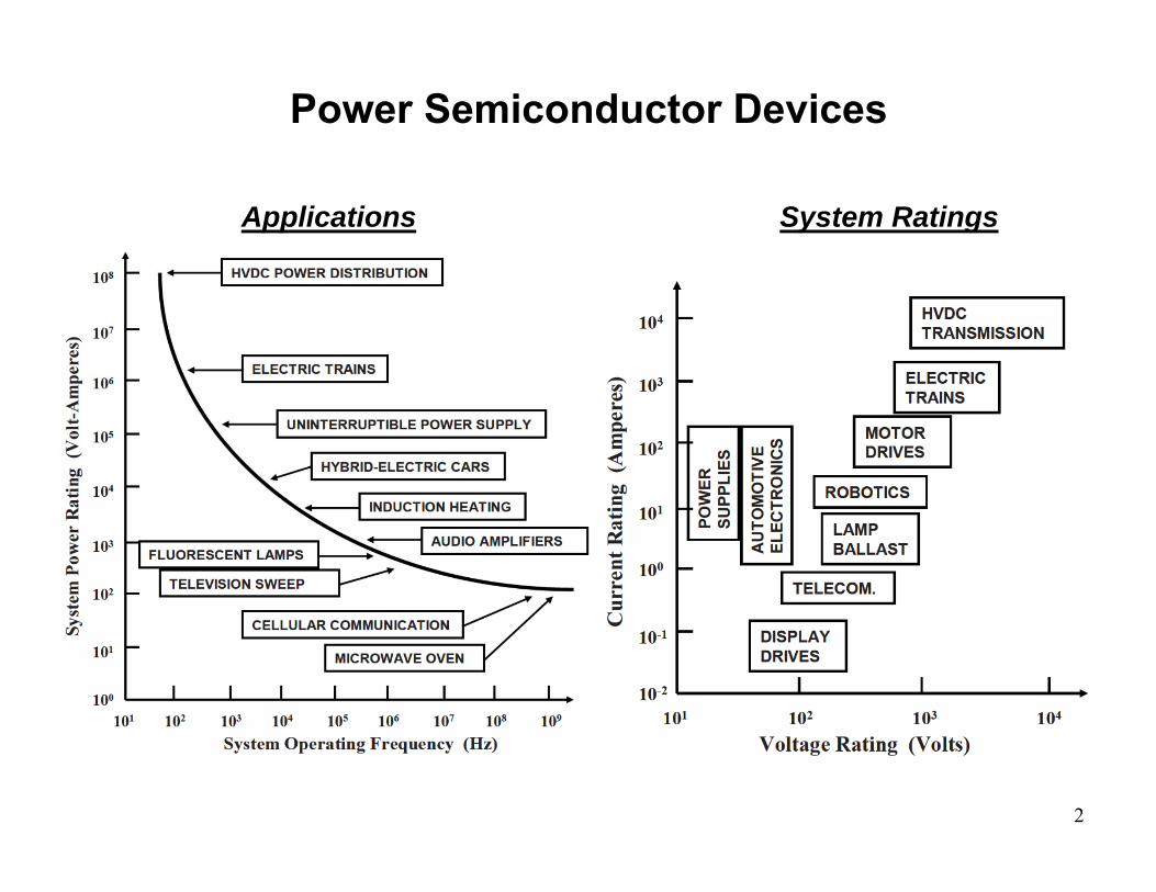
Power Semiconductor Devices
Applications System Ratings
3
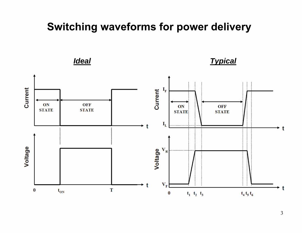
Switching waveforms for power delivery
Ideal Typical
4
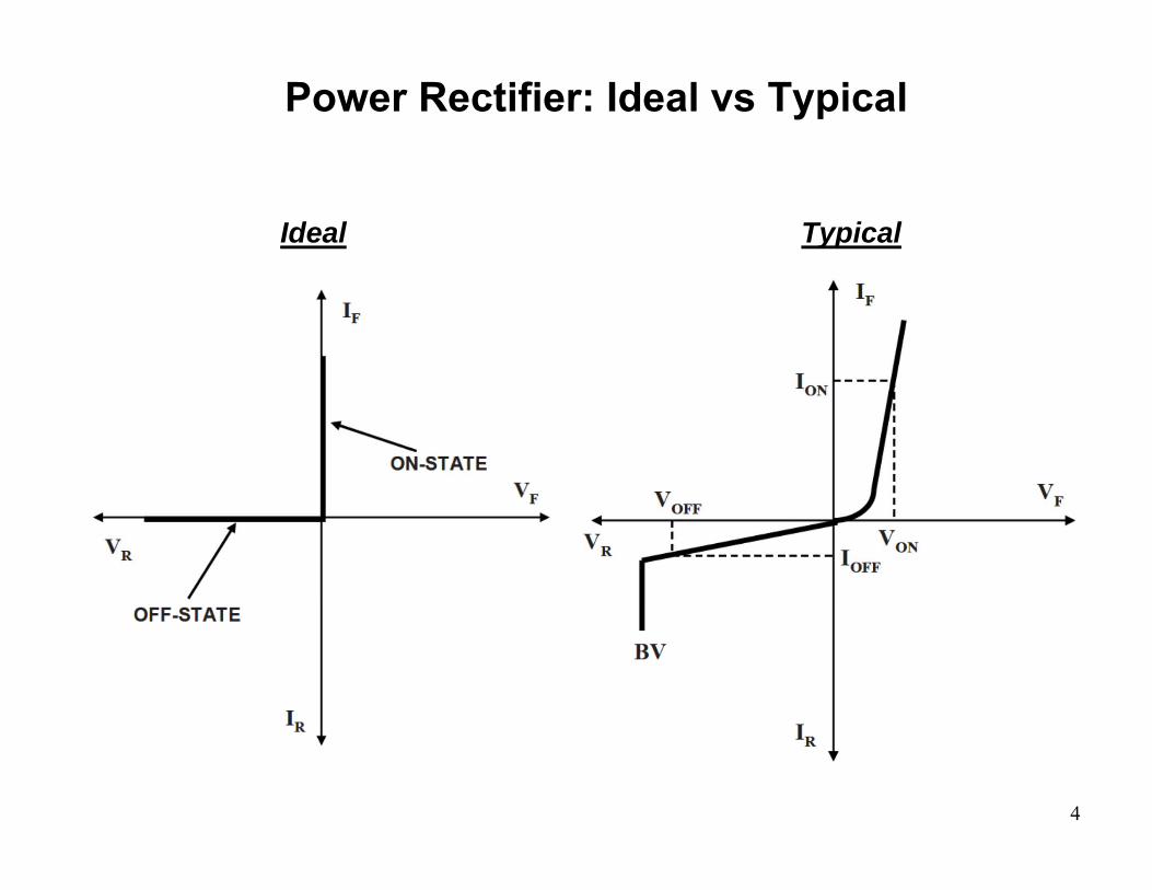
Power Rectifier: Ideal vs Typical
Ideal Typical
5
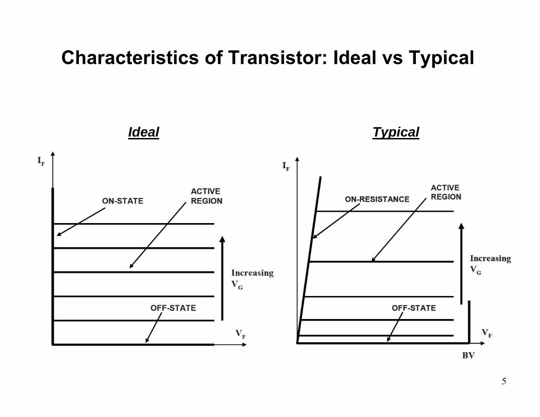
Characteristics of Transistor: Ideal vs Typical
Ideal Typical
6
Unipolar power devices vs Bipolar power devices
Bipolar power devices operate with the injection of minority carriersduring on-state current flow. These carriers must be removed whenswitching the device from the on-state to the off-state. This isaccomplished by either charge removal via the gate drive current or viathe electron-hole recombination process. These processes introducesignificant power losses that degrade the power management efficiency.It is therefore preferable to utilize unipolar current conduction in apower device.
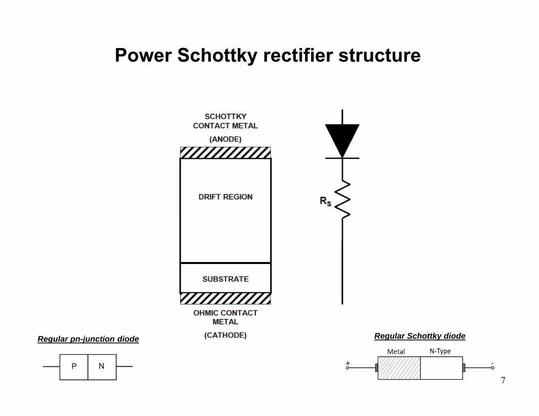
The commonly used unipolar power diode structure is the Schottkyrectifier.
The most commonly used unipolar power transistor is the powerMOSFET.
The commonly available silicon power bipolar devices are the bipolartransistor and the gate turn-off thyristor (GTO).
7
Power Schottky rectifier structure
Regular Schottky diodeRegular pn-junction diode
8
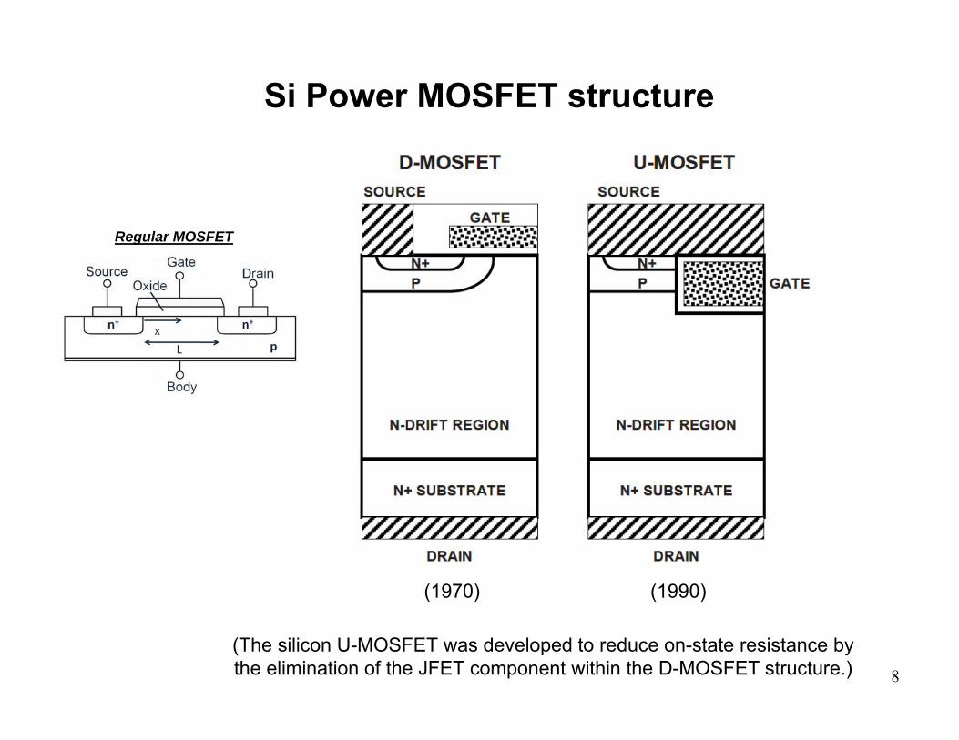
Si Power MOSFET structure
Regular MOSFET
(1970) (1990)
(The silicon U-MOSFET was developed to reduce on-state resistance by the elimination of the JFET component within the D-MOSFET structure.)
9
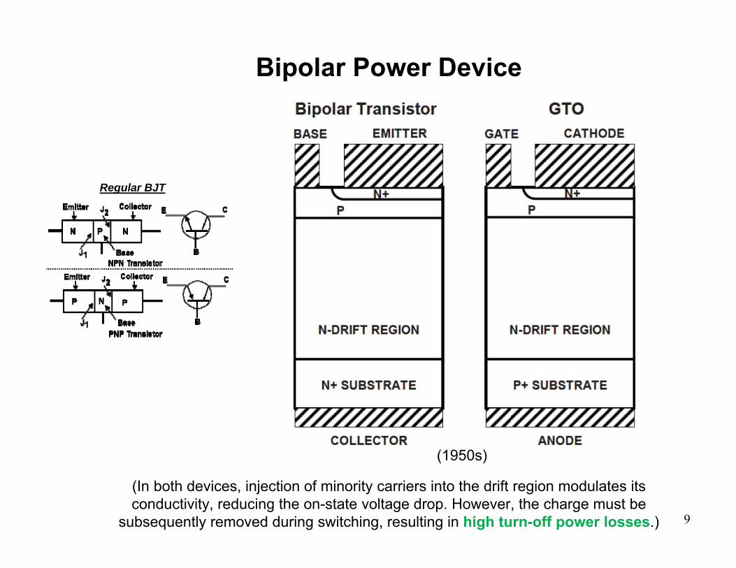
Bipolar Power Device
Regular BJT
(1950s)
(In both devices, injection of minority carriers into the drift region modulates its conductivity, reducing the on-state voltage drop. However, the charge must be
subsequently removed during switching, resulting in high turn-off power losses.)
10
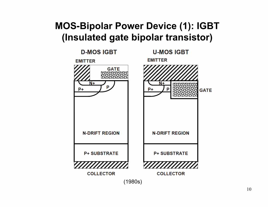
MOS-Bipolar Power Device (1): IGBT (Insulated gate bipolar transistor)
(1980s)
11
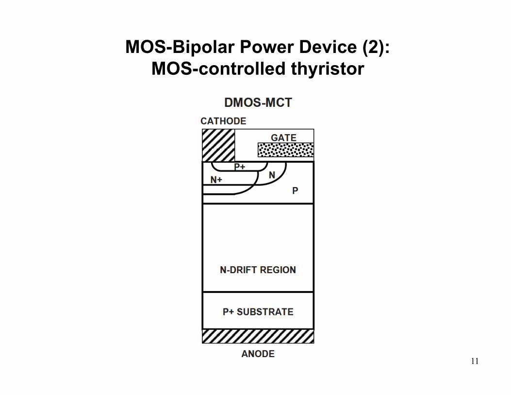
MOS-Bipolar Power Device (2): MOS-controlled thyristor
12
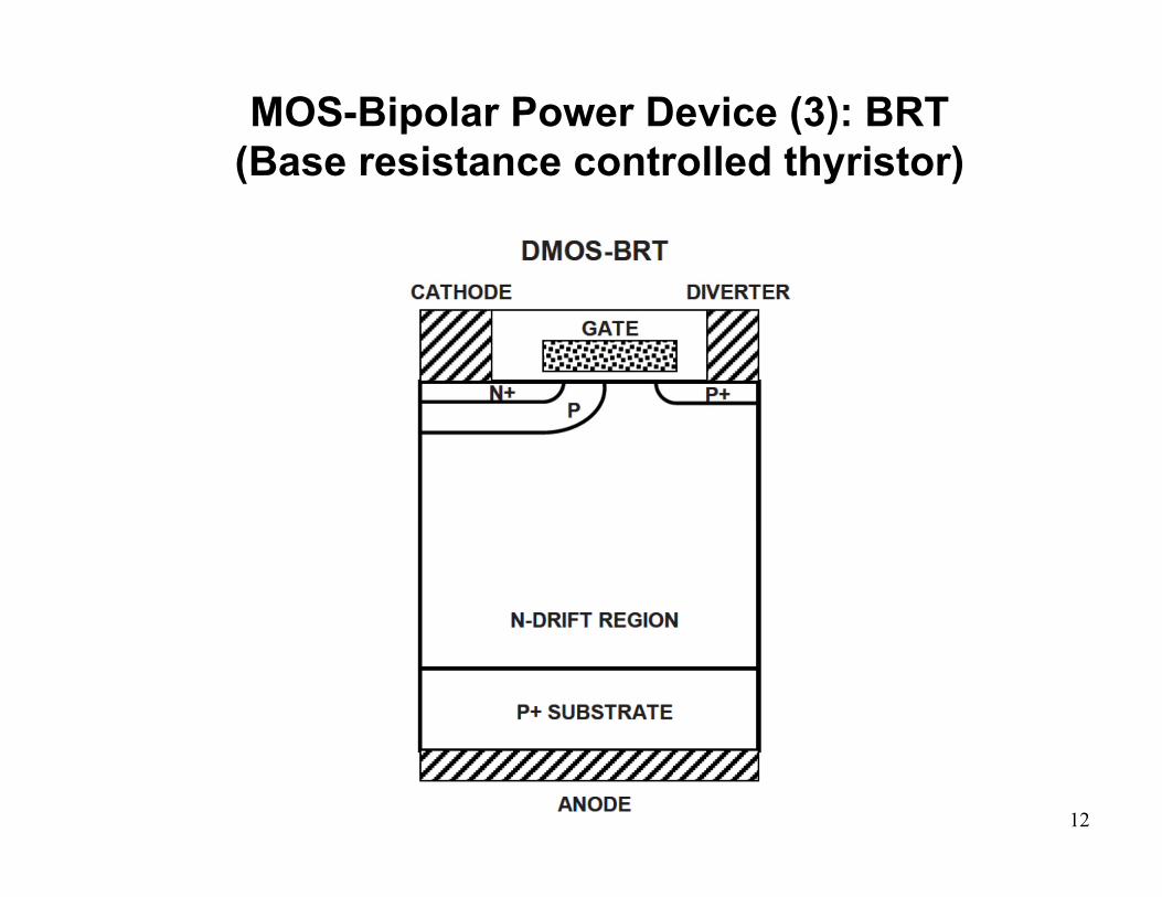
MOS-Bipolar Power Device (3): BRT (Base resistance controlled thyristor)
13
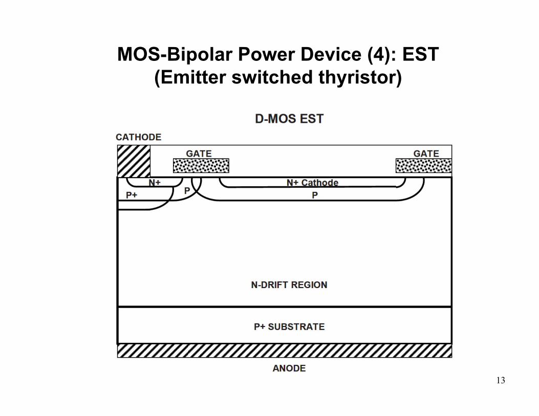
MOS-Bipolar Power Device (4): EST (Emitter switched thyristor)
14
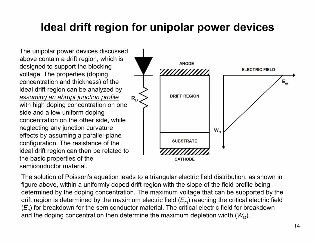
Ideal drift region for unipolar power devices
The unipolar power devices discussed above contain a drift region, which is designed to support the blocking voltage. The properties (doping concentration and thickness) of the ideal drift region can be analyzed by assuming an abrupt junction profilewith high doping concentration on one side and a low uniform doping concentration on the other side, while neglecting any junction curvature effects by assuming a parallel-plane configuration. The resistance of the ideal drift region can then be related to the basic properties of the semiconductor material.The solution of Poisson’s equation leads to a triangular electric field distribution, as shown in figure above, within a uniformly doped drift region with the slope of the field profile being determined by the doping concentration. The maximum voltage that can be supported by the drift region is determined by the maximum electric field (Em) reaching the critical electric field (Ec) for breakdown for the semiconductor material. The critical electric field for breakdown and the doping concentration then determine the maximum depletion width (WD).
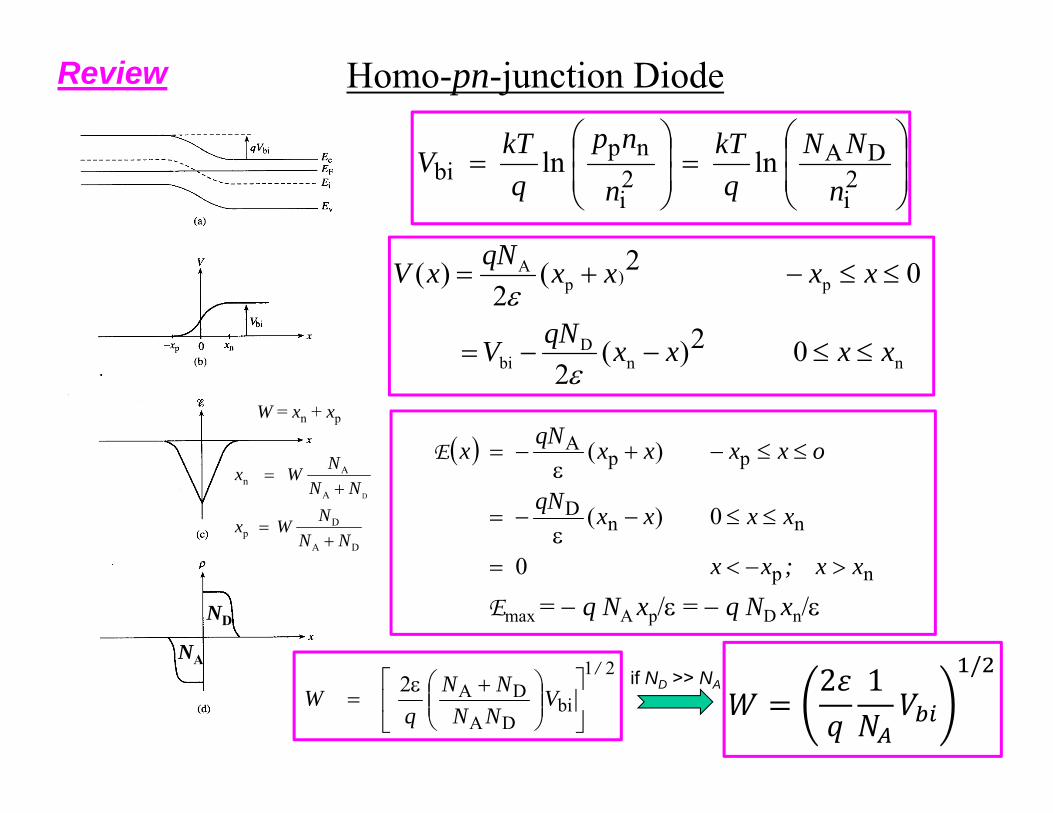
Homo-pn-junction Diode
2
i
DA2i
npbi lnln
nNN
qkT
n
npq
kTV
nnD
bi
p)pA
02)(2
02(2
)(
xxxxqNV
xxxxqNxV
np
nnD
ppA
0
0)(
)(
xx;xx
xxxxqN
oxxxxqNx
E
Emax = q NA xp/ = q ND xn/
NA
ND
DA
Dp
A
An
D
NNNWx
NNNWx
W = xn + xp
21
biDA
DA2/
VNNNN
qW
Review
2 1 /if ND >> NA
16
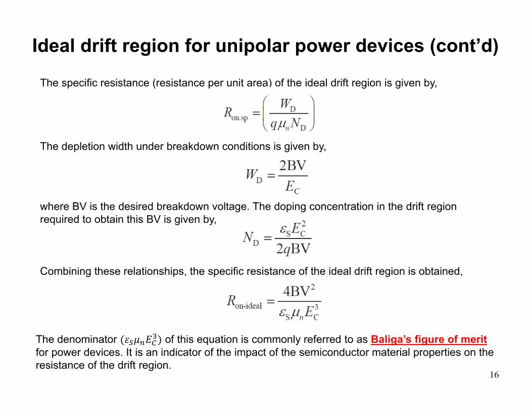
Ideal drift region for unipolar power devices (cont’d)
The specific resistance (resistance per unit area) of the ideal drift region is given by,
The depletion width under breakdown conditions is given by,
where BV is the desired breakdown voltage. The doping concentration in the drift region required to obtain this BV is given by,
Combining these relationships, the specific resistance of the ideal drift region is obtained,
The denominator of this equation is commonly referred to as Baliga’s figure of meritfor power devices. It is an indicator of the impact of the semiconductor material properties on the resistance of the drift region.
17
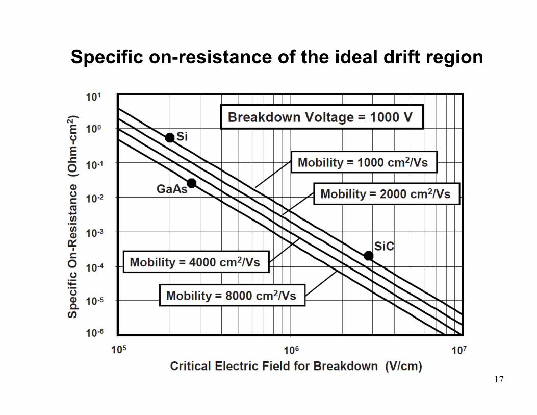
Specific on-resistance of the ideal drift region
18
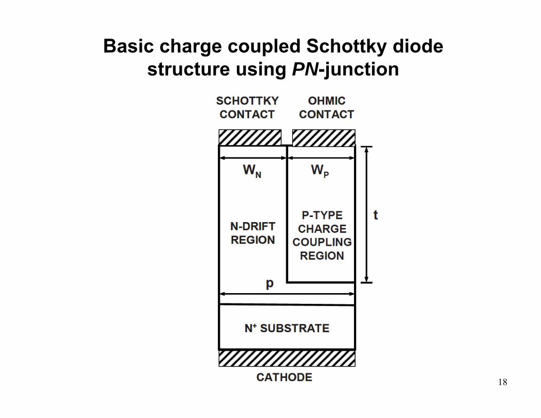
Basic charge coupled Schottky diode structure using PN-junction
19
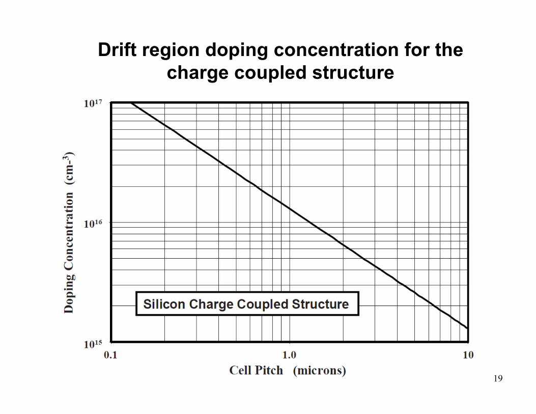
Drift region doping concentration for the charge coupled structure
20
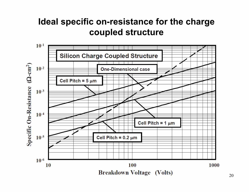
Ideal specific on-resistance for the charge coupled structure
21
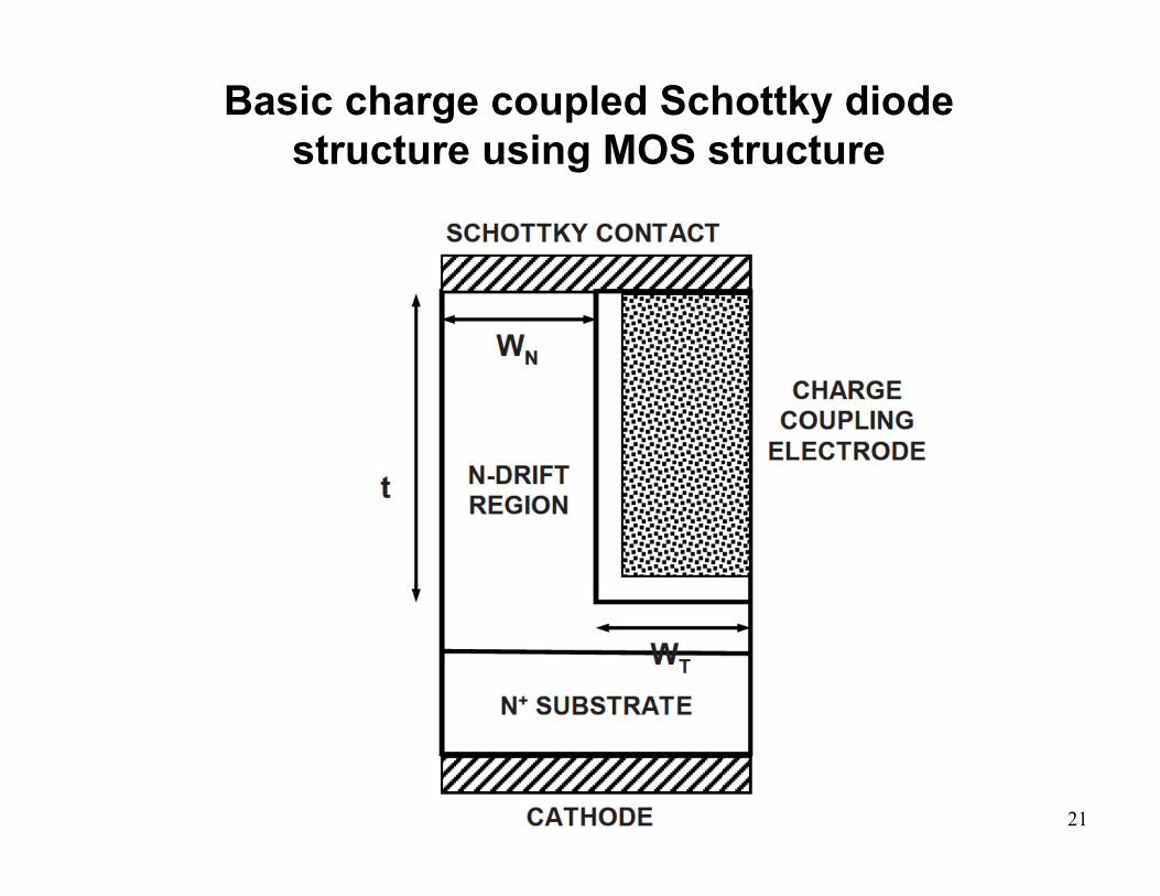
Basic charge coupled Schottky diode structure using MOS structure
22
Summary
The desired characteristics for power semiconductor rectifiersand transistors have been reviewed in this chapter. Thecharacteristics of typical silicon power devices have beencompared with those for the ideal case. Various unipolar andbipolar power device structures have been briefly introducedhere. Only the basic power device structures are discussed inthis book because of space constraints.
23
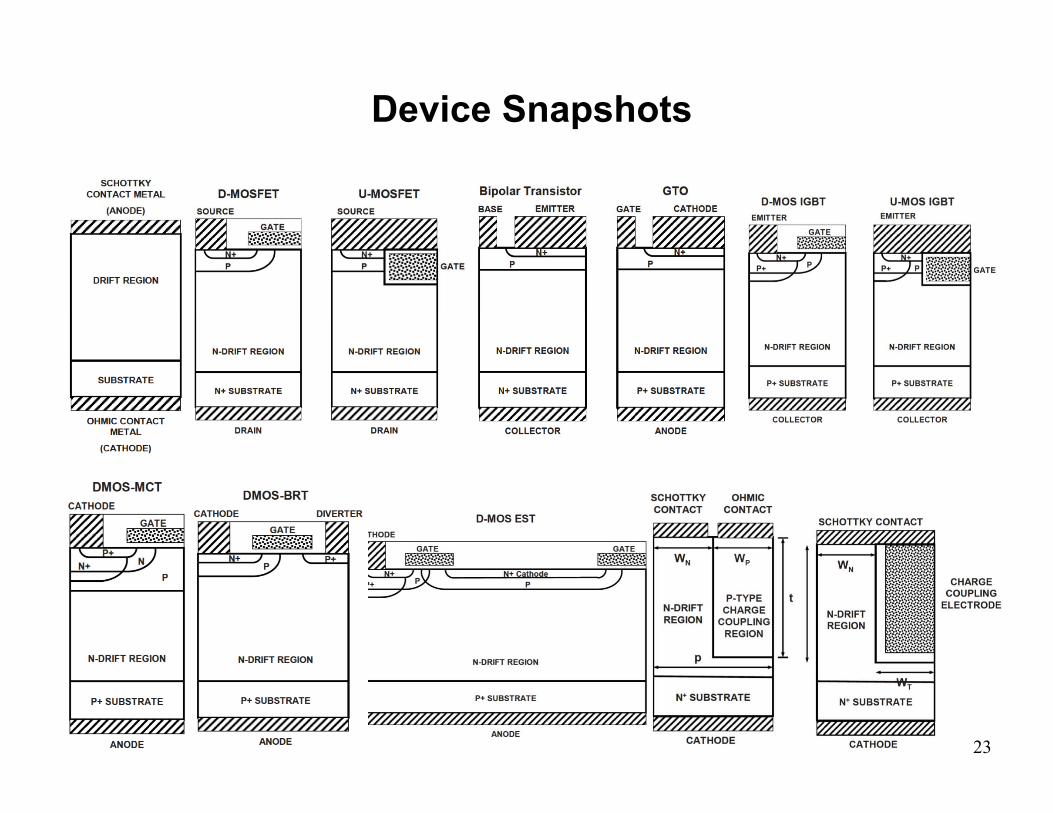
Device Snapshots