Embed Size (px)
Citation preview
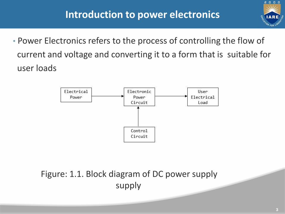
Introduction to power electronics
• Power Electronics refers to the process of controlling the flow of
current and voltage and converting it to a form that is suitable for
user loads
3
Figure: 1.1. Block diagram of DC power supplysupply
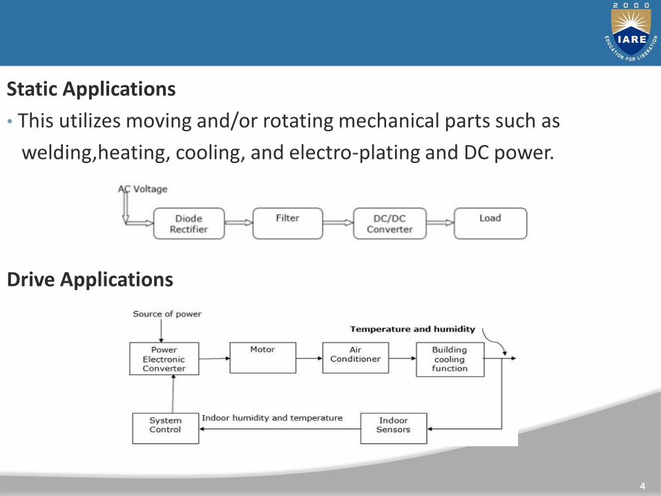
Static Applications
• This utilizes moving and/or rotating mechanical parts such as
welding,heating, cooling, and electro-plating and DC power.
Drive Applications
4
A power electronic system converts electrical energy from one form to another and ensures the following is achieved
1. Maximum efficiency2. Maximum reliability3. Maximum availability4. Minimum cost5. Least weight6. Small size
5
Types of power electronic converters
1. Rectifiers (AC to DC converters): These converters convert constant
ac voltage to variable dc output voltage.
2. Choppers (DC to DC converters): Dc chopper converts fixed dc
voltage to a controllable dc output voltage.
3. Inverters (DC to AC converters): An inverter converts fixed dc
voltage to a variable ac output voltage.
4. AC voltage controllers: These converters converts fixed ac voltage to
a variable ac output voltage at same frequency.
5. Cycloconverters: These circuits convert input power at one
frequency to output power at a different frequency through on6e
stage conversion.
6
Power semiconductor devices
1. Power Diodes.
2. Power transistors (BJT's).
3. Power MOSFETS.
4. IGBT's.
5. Thyristors
7
Thyristors – Silicon Controlled Rectifiers
• A silicon controlled rectifier or semiconductor-controlled rectifier is a
four-layer solidstate current-controlling device.
• The name "silicon controlled rectifier" is General Electric's trade name
for a type of thyristor.
8
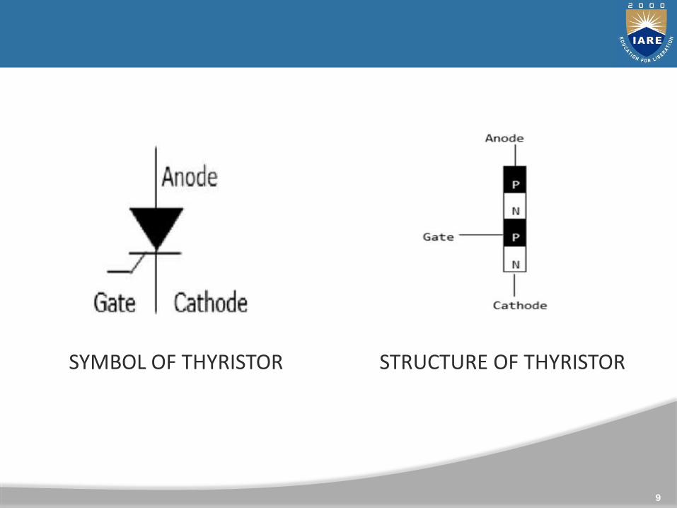
SYMBOL OF THYRISTOR
9
SYMBOL OF THYRISTOR STRUCTURE OF THYRISTOR
10
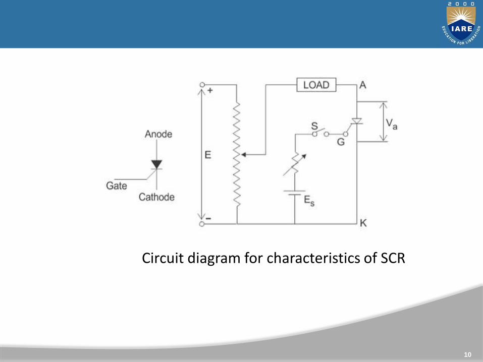
Circuit diagram for characteristics of SCR
11
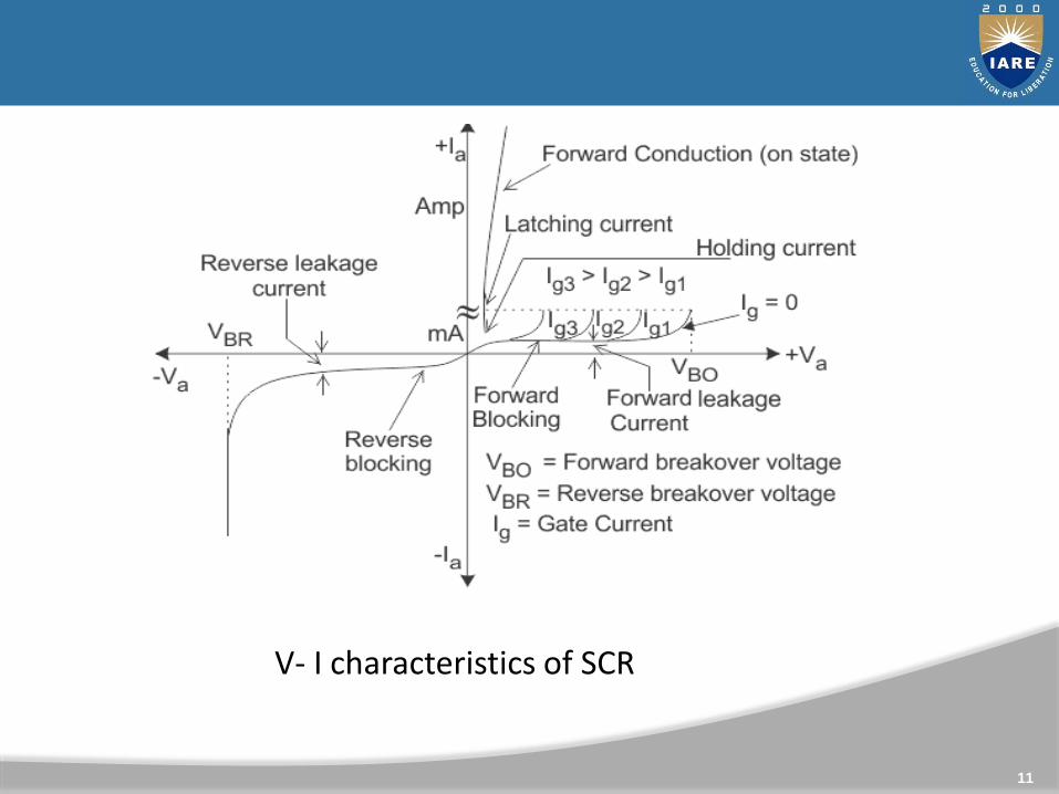
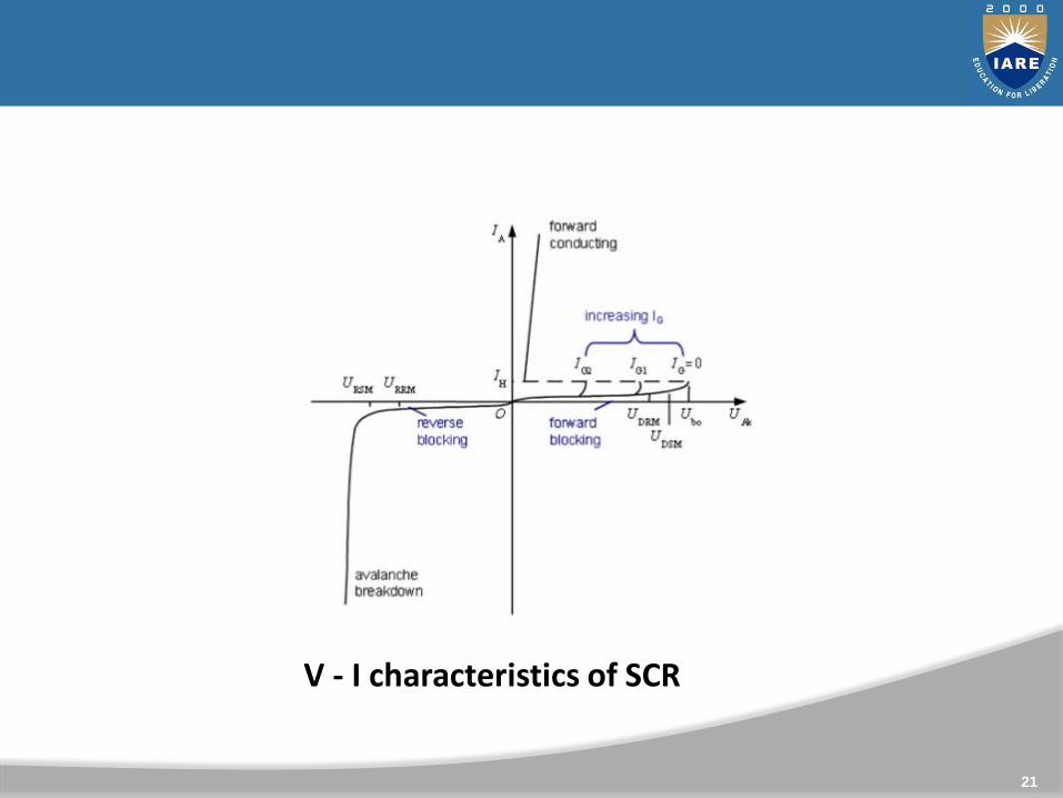
V- I characteristics of SCR
Two transistor analogy of SCR
• Basic operating principle of SCR, can be easily understood by the two
transistor model of SCR or analogy of silicon controlled rectifier, as it is
also a combination of P and N layers, shown in figure below
12
13
Two transistors connection
• The anode current of the thyristor in terms of transistor parameters is
Where
• α1 and α2 are current gains of the two transistors
• ICBO1 and ICBO2 are leakage currents of the two transistors
14
Turn on methods of SCR
• The turning on Process of the SCR is known as Triggering. In other
Words, turning the SCR from Forward-Blocking state to Forward-
Conduction state is known as Triggering. The various methods of SCR
triggering are discussed here.
The various SCR triggering methods are
• Forward Voltage Triggering
• Thermal or Temperature Triggering
• Radiation or Light triggering
• dv/dt Triggering
• Gate Triggering
15
Forward Voltage Triggering
• In this mode, an additional forward voltage is applied between anode
and cathode.
• When the anode terminal is positive with respect to cathode (VAK),
Junction J1 and J3 is forward biased and junction J2 is reverse biased.
• No current flow due to depletion region in J2 is reverse biased (except
leakage current).
• As VAK is further increased, at a voltage VBO (Forward Break Over
Voltage) the junction J2 undergoes avalanche breakdown and so a
current flows and the device tends to turn ON
16
Thermal (or) Temperature Triggering
• The width of depletion layer of SCR decreases with increase in junction
temperature.
• Therefore in SCR when VAR is very near its breakdown voltage, the
device is triggered by increasing the junction temperature.
• By increasing the junction temperature the reverse biased junction
collapses thus the device starts to conduct.
17
Radiation Triggering (or) Light Triggering
• For light triggered SCRs a special terminal niche is made inside the
inner P layer instead of gate terminal.
• When light is allowed to strike this terminal, free charge carriers are
generated.
• When intensity of light becomes more than a normal value, the
thyristor starts conducting.
• This type of SCRs are called as LASCR
18
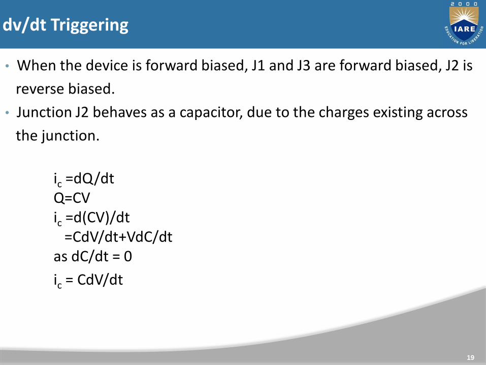
dv/dt Triggering
• When the device is forward biased, J1 and J3 are forward biased, J2 is
reverse biased.
• Junction J2 behaves as a capacitor, due to the charges existing across
the junction.
ic =dQ/dtQ=CVic =d(CV)/dt
=CdV/dt+VdC/dtas dC/dt = 0
ic = CdV/dt
19
Gate Triggering
• This is most widely used SCR triggering method.
• Applying a positive voltage between gate and cathode can Turn ON a
forward biased thyristor.
• When a positive voltage is applied at the gate terminal, charge carriers
are injected in the inner P-layer, thereby reducing the depletion layer
thickness.
• As the applied voltage increases, the carrier injection increases,
therefore the voltage at which forward break-over occurs decreases.
20
21
V - I characteristics of SCR
The turn OFF process of an SCR is called commutation. The term
commutation means the transfer of currents from one path to
another. So the commutation circuit does this job by reducing the
forward current to zero so as to turn OFF the SCR or Thyristor.
To turn OFF the conducting SCR the below conditions must
be satisfied.
The anode or forward current of SCR must be reduced to
zero or below the level of holding current and then,
A sufficient reverse voltage must be applied across the SCR
to regain its forward blocking state.
22
Turn off methods of SCR
SCR Turn OFF Methods
The reverse voltage which causes to commutate the SCR is
called commutation voltage. Depending on the commutation
voltage located, the commutation methods are classified into
two major types.
Those are 1) Forced commutation and 2) Natural
commutation. Let us discuss in brief about these methods.
23
Class A Commutation
24
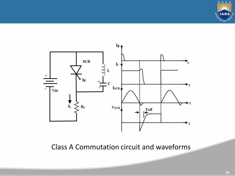
Class A Commutation circuit and waveforms
This is also known as self commutation, or resonant
commutation, or load commutation. In this commutation, the
source of commutation voltage is in the load. This load must
be an under damped R-L-C supplied with a DC supply so that
natural zero is obtained.
The commutating components L and C are connected either
parallel or series with the load resistance R as shown below
with waveforms of SCR current, voltage and capacitor
voltage.
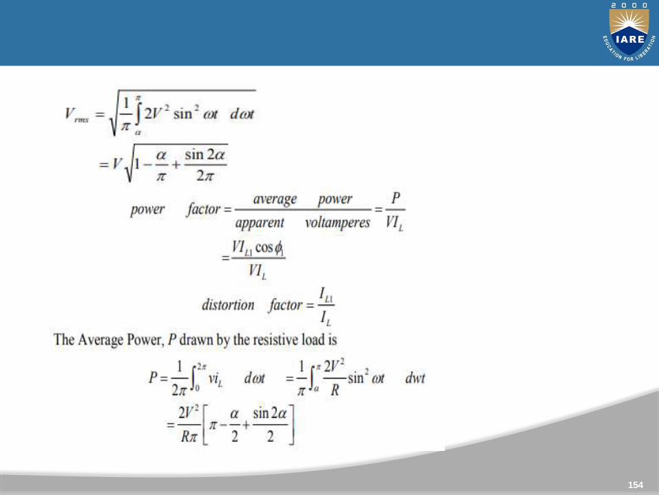
25
Class B Commutation
26
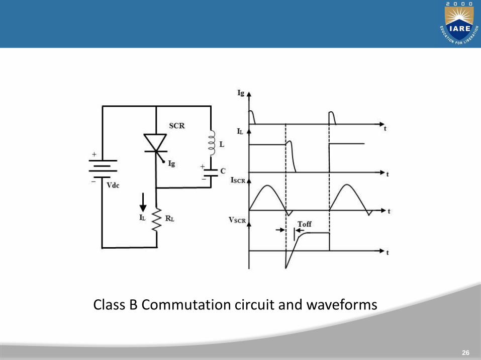
Class B Commutation circuit and waveforms
This is also a self commutation circuit in which commutation
of SCR is achieved automatically by L and C components,
once the SCR is turned ON. In this, the LC resonant circuit is
connected across the SCR but not in series with load as in
case of class A commutation and hence the L and C
components do not carry the load current
27
In this commutation method, the main SCR is to be
commutated is connected in series with the load and an
additional or complementary SCR is connected in parallel
with main SCR. This method is also called as complementary
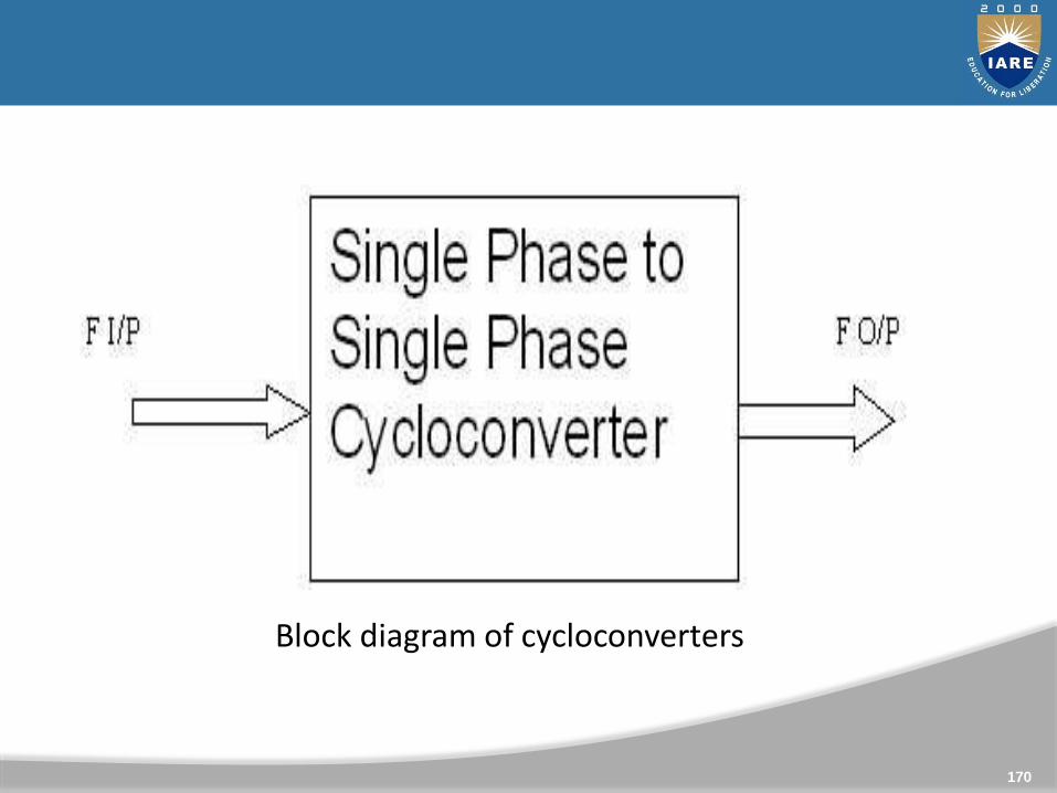
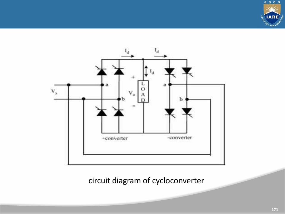
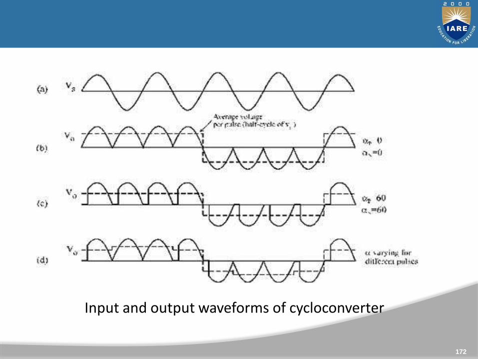
commutation.
In this , SCR turns OFF with a reverse voltage of a charged
capacitor. The figure below shows the complementary
commutation with appropriate waveforms.
28
Class C Commutation
29
Class C Commutation circuit and waveforms
This is also called as auxiliary commutation because it uses an
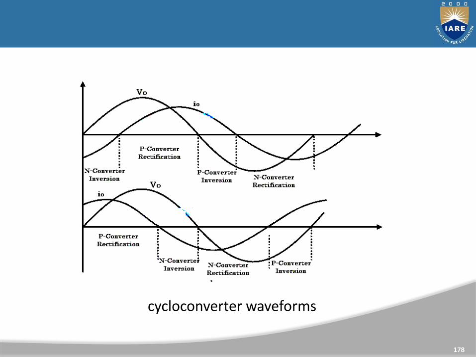
auxiliary SCR to switch the charged capacitor. In this, the
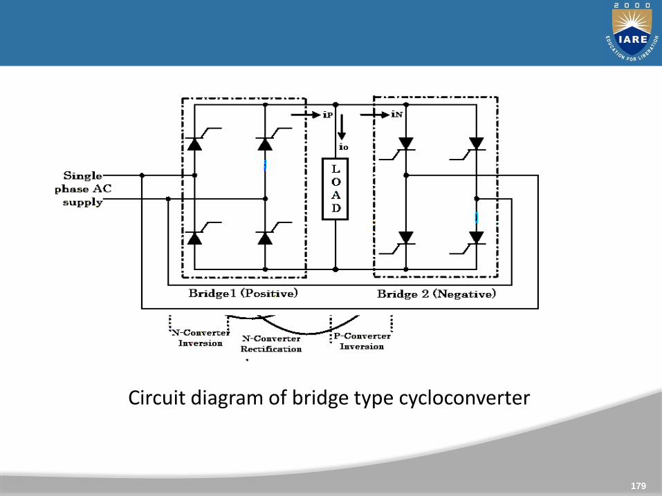
main SCR is commutated by the auxiliary SCR. The main SCR
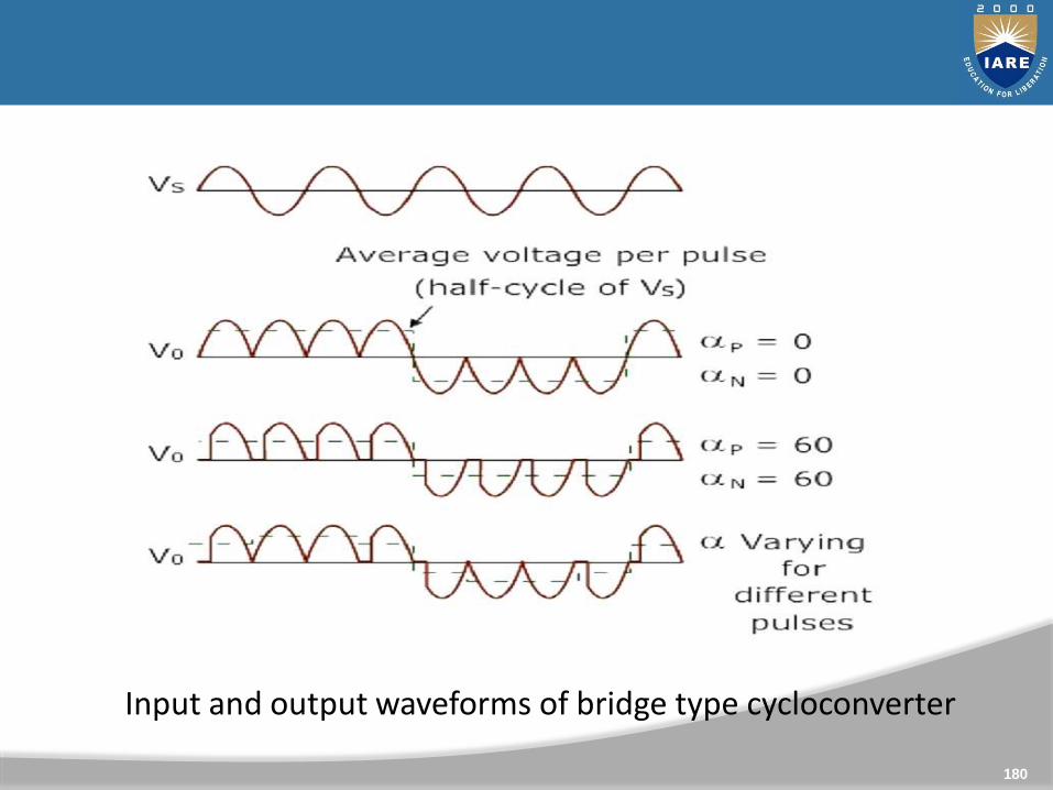
with load resistance forms the power circuit while the diode
D, inductor L and SCR2 forms the commutation circuit.
This commutation method is mainly used in inverters and
also used in the Jones chopper circuit.
30
Class D Commutation
31
Class D Commutation circuit and waveforms
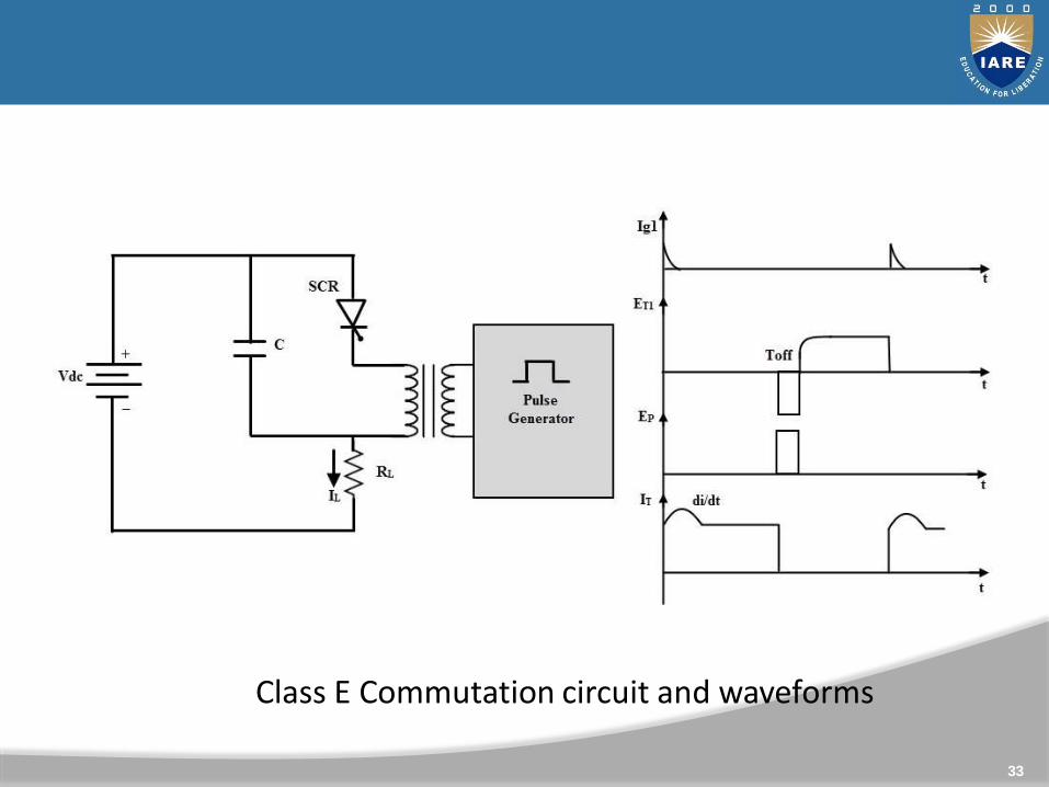
This is also known as external pulse commutation. In this, an
external pulse source is used to produce the reverse voltage
across the SCR. The circuit below shows the class E
commutation circuit which uses a pulse transformer to
produce the commutating pulse and is designed with tight
coupling between the primary and secondary with a small air
gap.
32
Class E Commutation
33
Class E Commutation circuit and waveforms
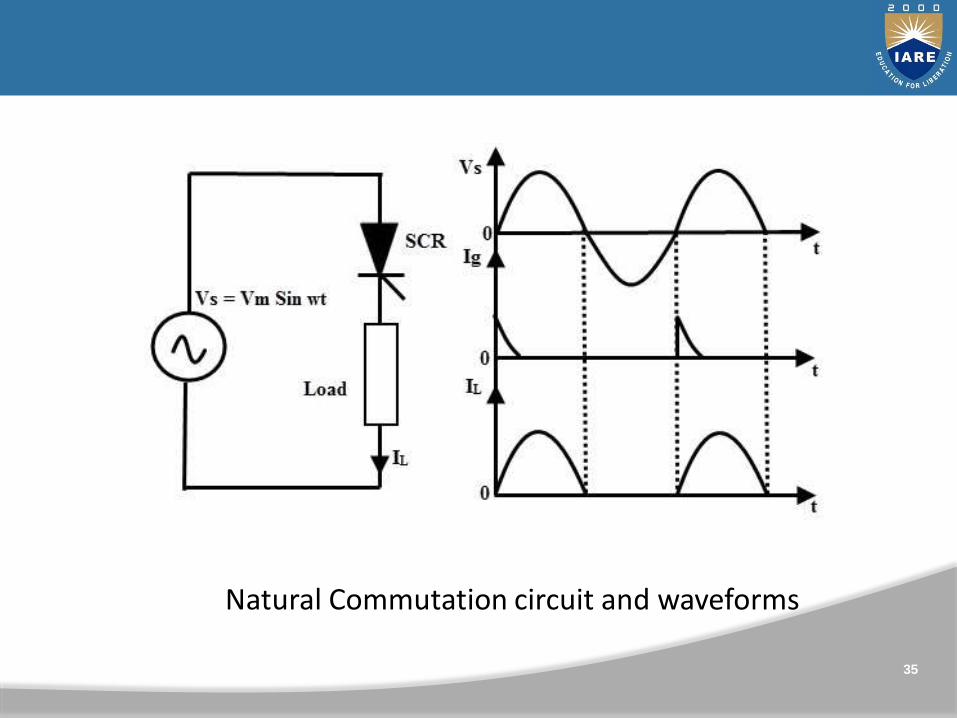
In natural commutation, the source of commutation voltage
is the supply source itself. If the SCR is connected to an AC
supply, at every end of the positive half cycle the anode
current goes through the natural current zero and also
immediately a reverse voltage is applied across the SCR.
These are the conditions to turn OFF the SCR.
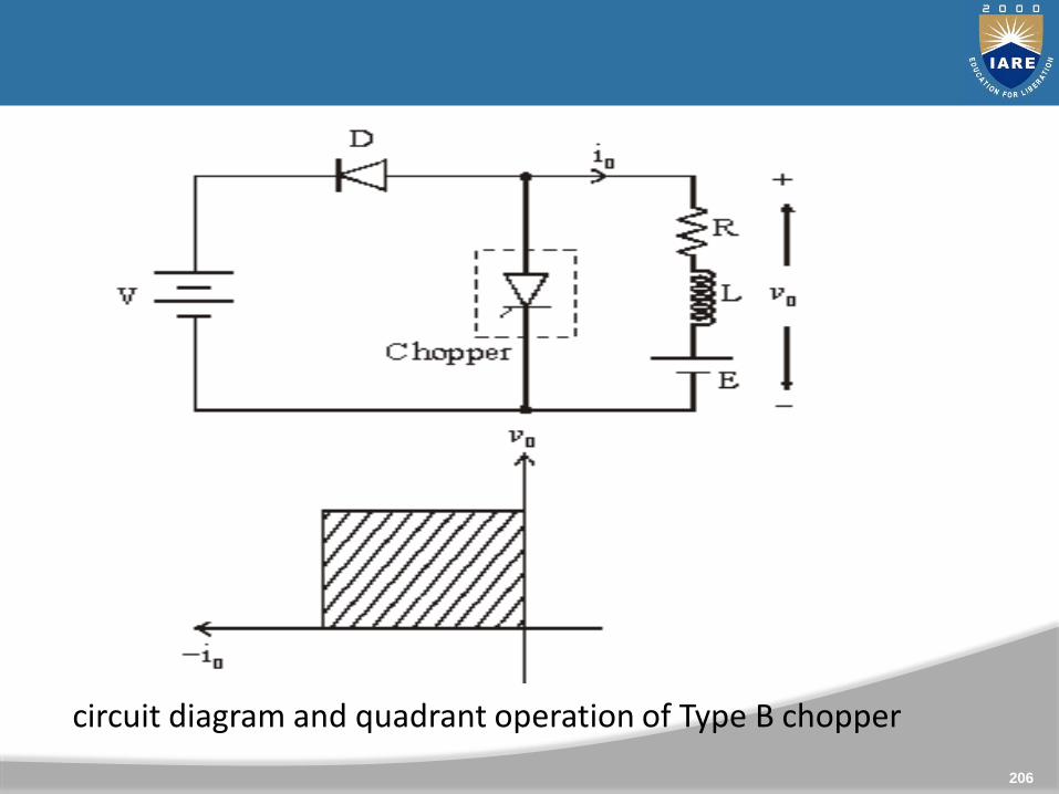
34
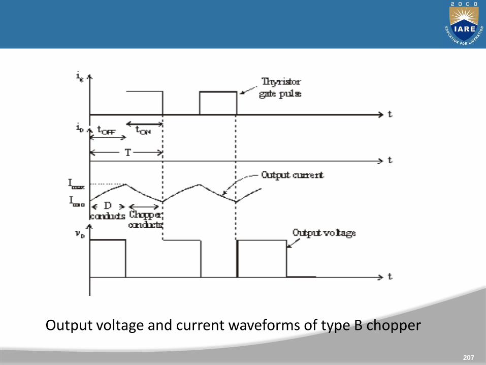
Natural Commutation
35
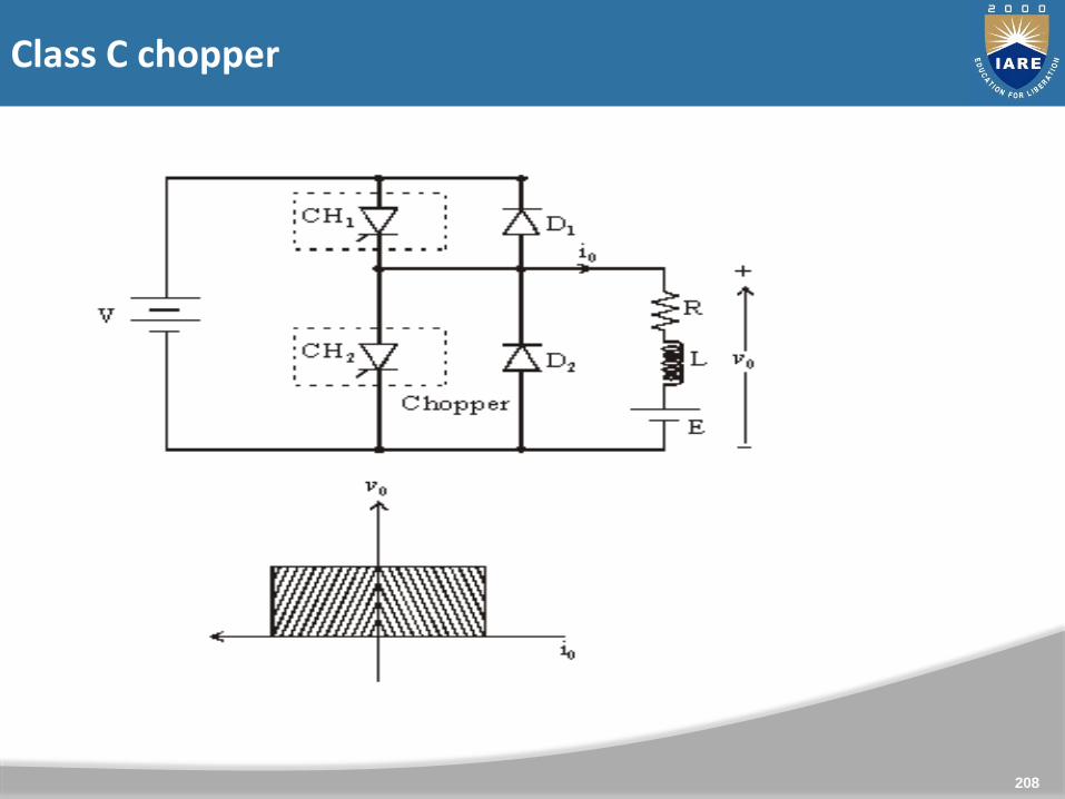
Natural Commutation circuit and waveforms
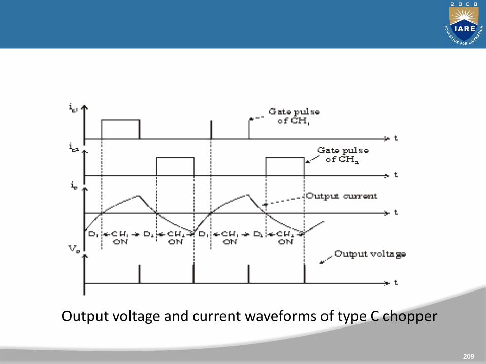
The transition of an SCR from forward conduction state toforward blocking state is called as turn OFF or commutation ofSCR. As we know that once the SCR starts conducting, the gatehas no control over it to bring back to forward blocking or OFFstate.
To turn OFF the SCR, the current must be reduced to a levelbelow the holding current of SCR. We have discussed variousmethods above to turn OFF the SCR in which SCR turn OFF isachieved by reducing the forward current to zero. But if we applythe forward voltage immediately after the current zero of SCR, itstarts conducting again even without gate triggering.
36
Dynamic Turn OFF Switching Characteristics
This is due to the presence of charge carriers in the four layers.Therefore, it is necessary to apply the reverse voltage, over a finitetime across the SCR to remove the charge carriers.
Hence the turn OFF time is defined as the time between theinstant the anode current becomes zero and the instant at whichthe SCR retains the forward blocking capability. The excess chargecarriers from the four layers must be removed to bring back theSCR to forward conduction mode.
This process takes place in two stages. In a first stage excesscarriers from outer layers are removed and in second stage excesscarriers in the inner two layers are to be recombined. Hence, thetotal turn OFF time tq is divided into two intervals; reverserecovery time trr and gate recovery time tgr.
tq = trr + tgr
37
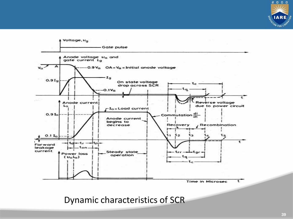
The figure below shows the switching characteristics of SCRduring turn ON and OFF. The time t1 to t3 is called as reverserecovery time; at the instant t1the anode current is zero andbuilds up in the reverse direction which is called as reverserecovery current. This current removes the excess charge carriersfrom outer layers during the time t1 to t3.
At instant t3, junctions J1 and J3 are able to block the reversevoltage but, the SCR is not yet able to block the forward voltagedue to the presence of excess charge carriers in junction J2. Thesecarriers can be disappeared only by the way of recombinationand this could be achieved by maintaining a reverse voltageacross the SCR.
38
39
Dynamic characteristics of SCR
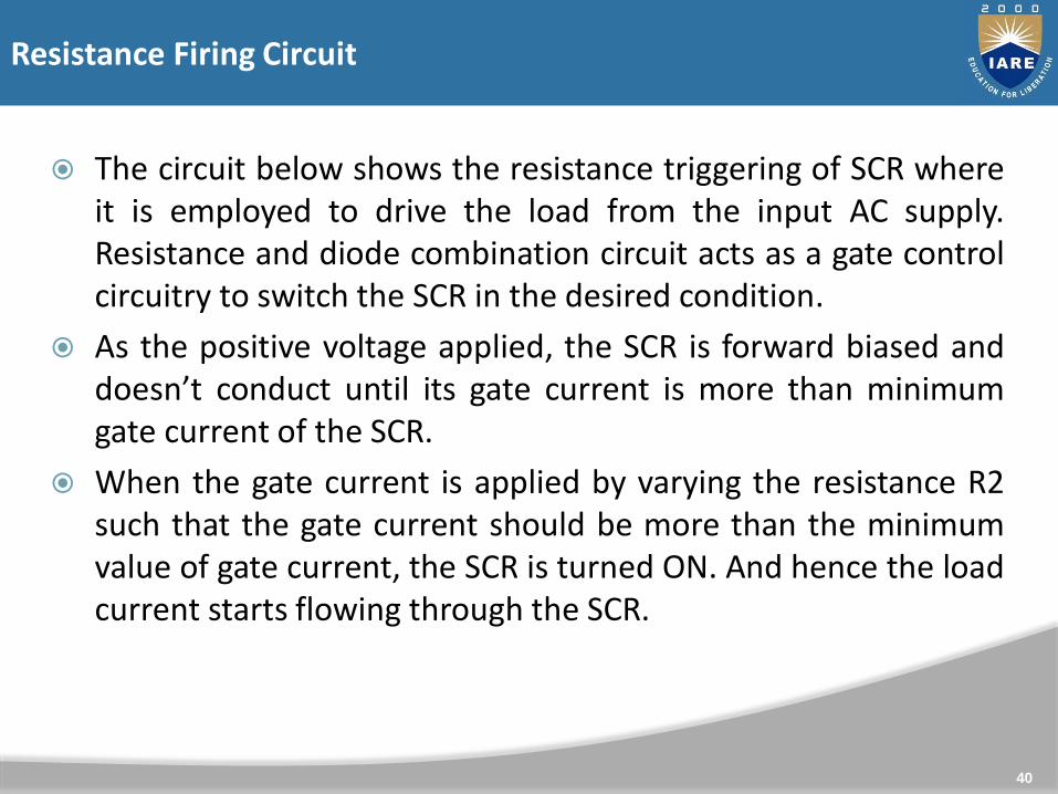
The circuit below shows the resistance triggering of SCR whereit is employed to drive the load from the input AC supply.Resistance and diode combination circuit acts as a gate controlcircuitry to switch the SCR in the desired condition.
As the positive voltage applied, the SCR is forward biased anddoesn’t conduct until its gate current is more than minimumgate current of the SCR.
When the gate current is applied by varying the resistance R2such that the gate current should be more than the minimumvalue of gate current, the SCR is turned ON. And hence the loadcurrent starts flowing through the SCR.
40
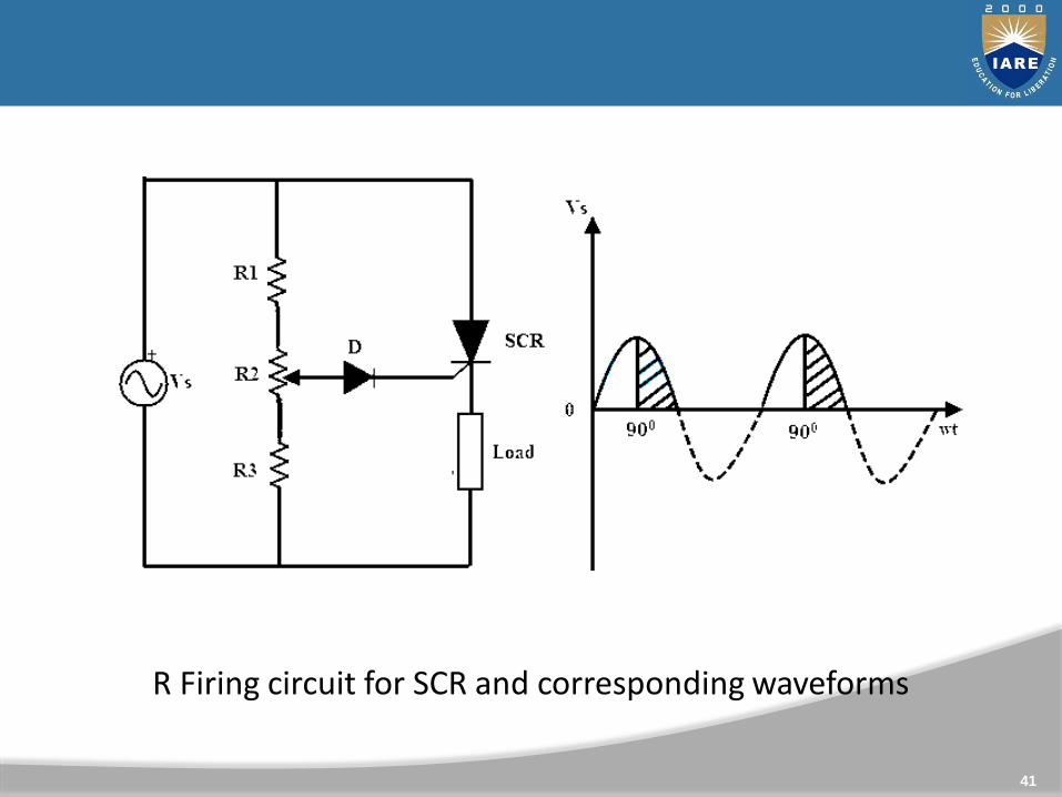
Resistance Firing Circuit
41
R Firing circuit for SCR and corresponding waveforms
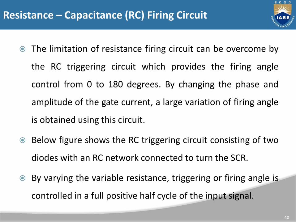
The limitation of resistance firing circuit can be overcome by
the RC triggering circuit which provides the firing angle
control from 0 to 180 degrees. By changing the phase and
amplitude of the gate current, a large variation of firing angle
is obtained using this circuit.
Below figure shows the RC triggering circuit consisting of two
diodes with an RC network connected to turn the SCR.
By varying the variable resistance, triggering or firing angle is
controlled in a full positive half cycle of the input signal.
42
Resistance – Capacitance (RC) Firing Circuit
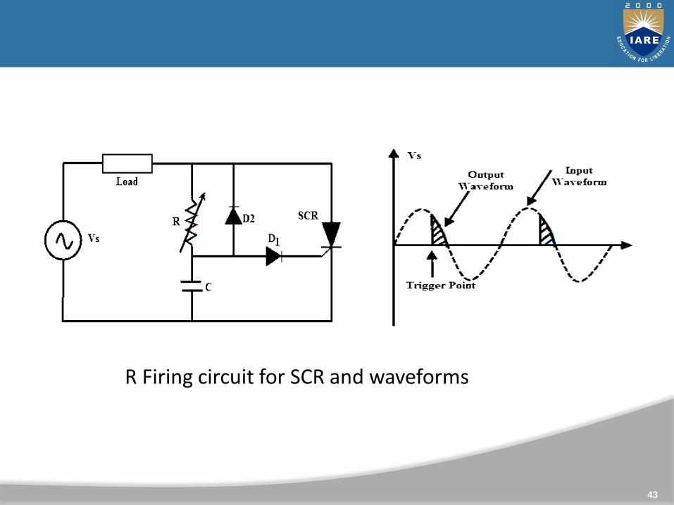
43
R Firing circuit for SCR and waveforms
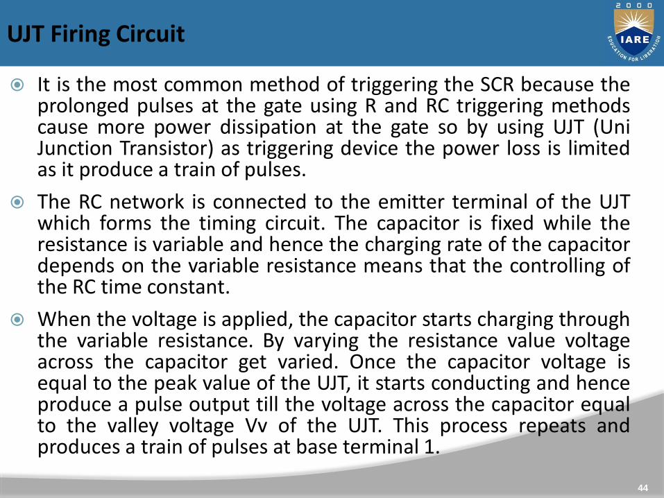
It is the most common method of triggering the SCR because theprolonged pulses at the gate using R and RC triggering methodscause more power dissipation at the gate so by using UJT (UniJunction Transistor) as triggering device the power loss is limitedas it produce a train of pulses.
The RC network is connected to the emitter terminal of the UJTwhich forms the timing circuit. The capacitor is fixed while theresistance is variable and hence the charging rate of the capacitordepends on the variable resistance means that the controlling ofthe RC time constant.
When the voltage is applied, the capacitor starts charging throughthe variable resistance. By varying the resistance value voltageacross the capacitor get varied. Once the capacitor voltage isequal to the peak value of the UJT, it starts conducting and henceproduce a pulse output till the voltage across the capacitor equalto the valley voltage Vv of the UJT. This process repeats andproduces a train of pulses at base terminal 1.
44
UJT Firing Circuit
45
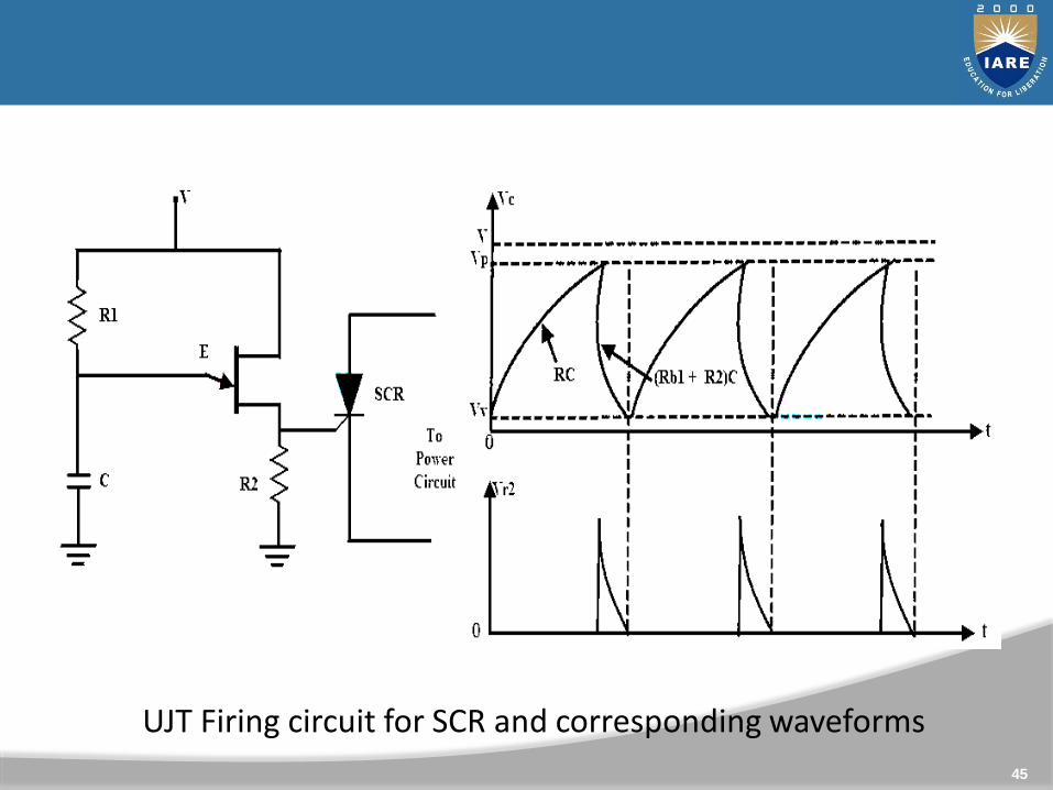
UJT Firing circuit for SCR and corresponding waveforms
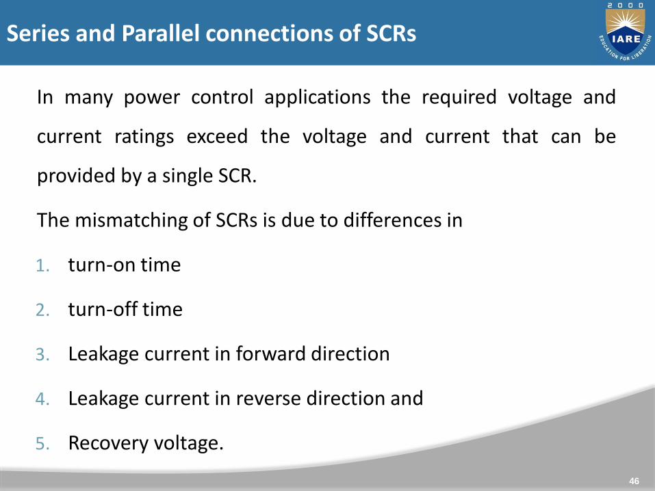
In many power control applications the required voltage and
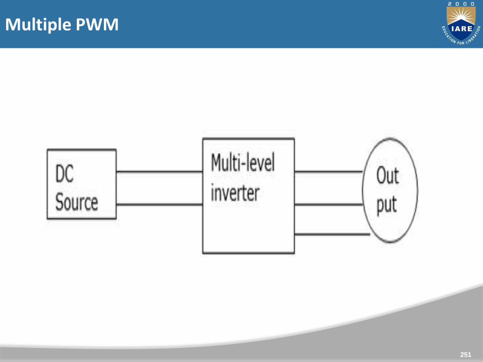
current ratings exceed the voltage and current that can be
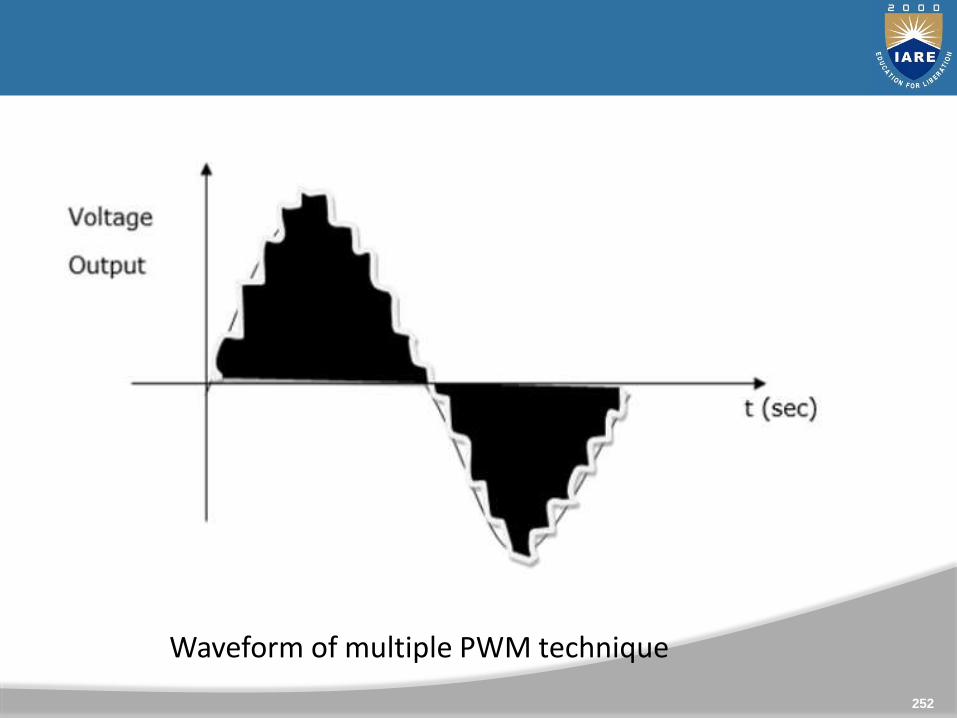
provided by a single SCR.
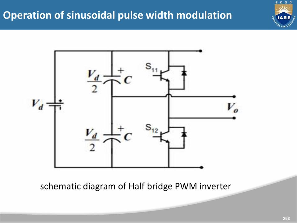
The mismatching of SCRs is due to differences in
1. turn-on time
2. turn-off time
3. Leakage current in forward direction
4. Leakage current in reverse direction and
5. Recovery voltage.
46
Series and Parallel connections of SCRs
Series Connection of an SCR
47
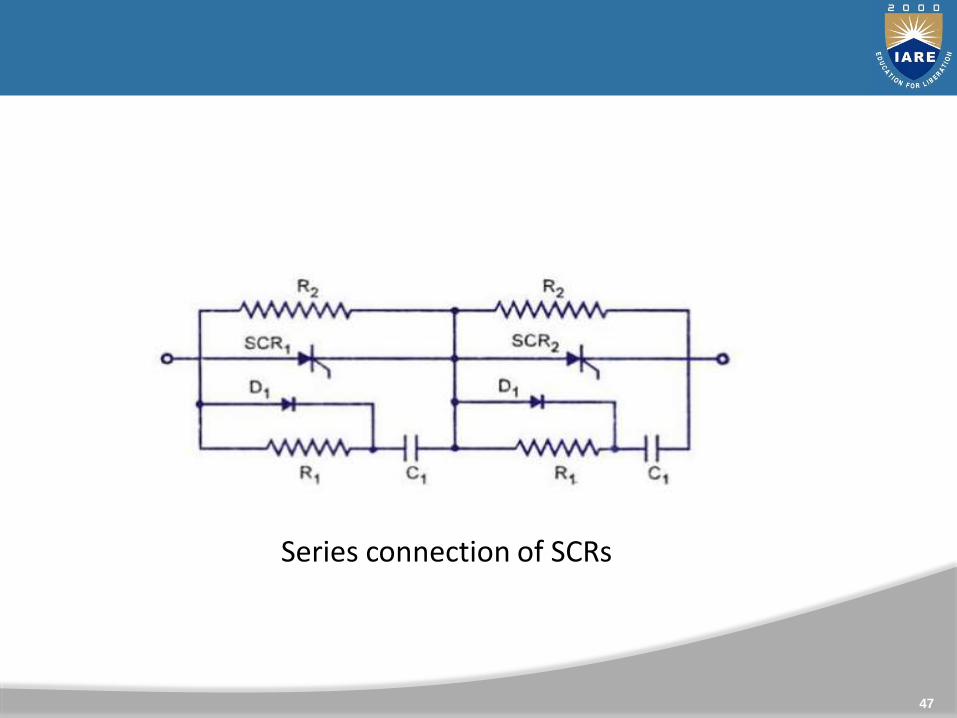
Series connection of SCRs
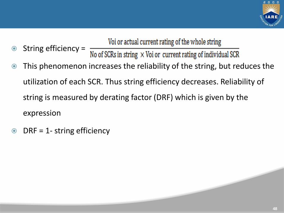
String efficiency =
This phenomenon increases the reliability of the string, but reduces the
utilization of each SCR. Thus string efficiency decreases. Reliability of
string is measured by derating factor (DRF) which is given by the
expression
DRF = 1- string efficiency
48
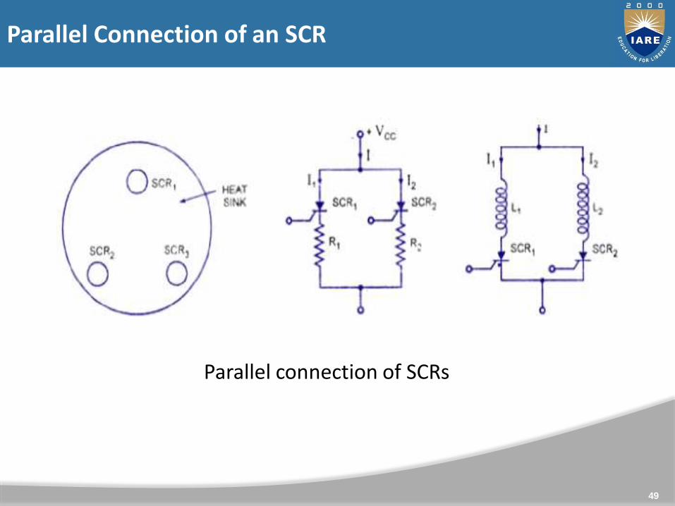
49
Parallel connection of SCRs
Parallel Connection of an SCR
When the load current exceeds the SCR current rating, SCRs are
connected in parallel to share the load current. But when SCRs are
operated in parallel, the current sharing between them may not be
proper. The device having lower dynamic resistance will tend to
share more current. This will raise the temperature of that
particular device in comparison to other, thereby reducing further
its dynamic resistance and increasing current through it. This
process is cumulative and continues till the device gets punctured.
50
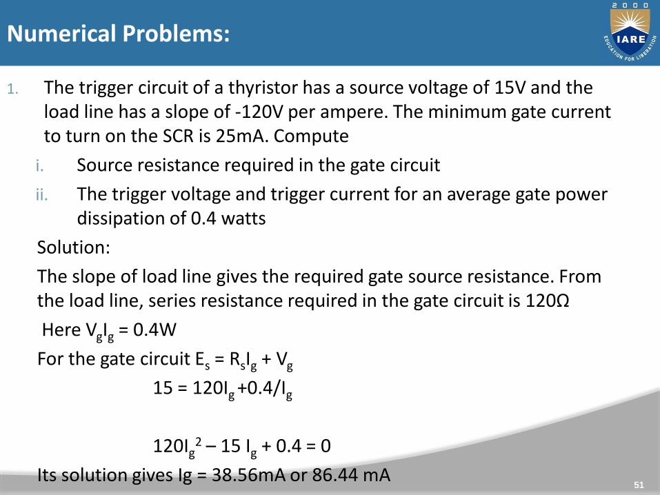
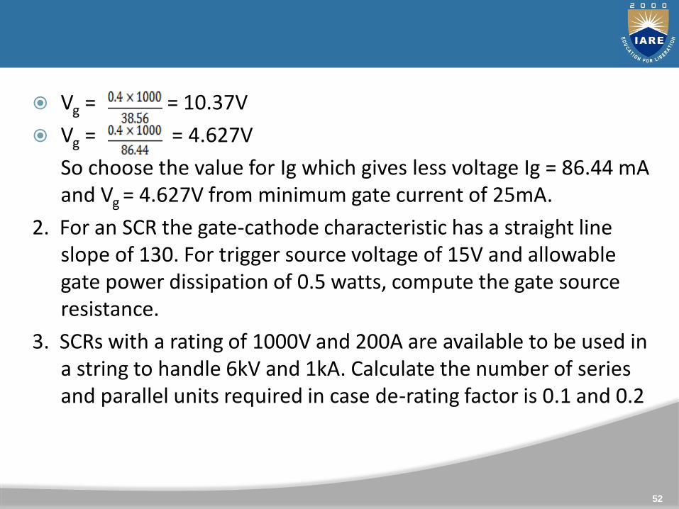
1. The trigger circuit of a thyristor has a source voltage of 15V and the load line has a slope of -120V per ampere. The minimum gate current to turn on the SCR is 25mA. Compute
i. Source resistance required in the gate circuit
ii. The trigger voltage and trigger current for an average gate power dissipation of 0.4 watts
Solution:
The slope of load line gives the required gate source resistance. From the load line, series resistance required in the gate circuit is 120Ω
Here VgIg = 0.4W
For the gate circuit Es = RsIg + Vg
15 = 120Ig +0.4/Ig
120Ig2 – 15 Ig + 0.4 = 0
Its solution gives Ig = 38.56mA or 86.44 mA51
Numerical Problems:
Cont..
Vg = = 10.37V
Vg = = 4.627V
So choose the value for Ig which gives less voltage Ig = 86.44 mAand Vg = 4.627V from minimum gate current of 25mA.
2. For an SCR the gate-cathode characteristic has a straight line slope of 130. For trigger source voltage of 15V and allowable gate power dissipation of 0.5 watts, compute the gate source resistance.
3. SCRs with a rating of 1000V and 200A are available to be used in a string to handle 6kV and 1kA. Calculate the number of series and parallel units required in case de-rating factor is 0.1 and 0.2
52
Due to overheating, over voltage, over current or excessive change involtage or current switching devices and circuit components may fail.From over current they can be protected by placing fuses at suitablelocations. Heat sinks and fans can be used to take the excess heat awayfrom switching devices and other components. Snubber circuits areneeded to limit the rate of change in voltage or current
Necessity of Using the Snubber Circuit
These are placed across the various switching devices like transistors,thyristors, etc. Switching from ON to OFF state results the impedanceof the device suddenly changes to the high value. But this allows asmall current to flow through the switch. This induces a large voltageacross the device. If this current reduced at faster rate more is theinduced voltage across the device and also if the switch is not capableof withstanding this voltage the switch becomes burn out. So auxiliarypath is needed to prevent this high induced voltage
53
Snubber circuit
There are many kinds of snubbers like RC, diode and solid state
snubbers but the most commonly used one is RC snubber circuit. This is
applicable for both the rate of rise control and damping.
This circuit is a capacitor and series resistor connected across a switch.
For designing the Snubber circuits. The amount of energy is to dissipate
in the snubber resistance is equal to the amount of energy is stored in
the capacitors. An RC Snubber placed across the switch can be used to
reduce the peak voltage at turn-off and to lamp the ring. An RC snubber
circuit can be polarized or non-polarized. If you assume the source has
negligible impedance, the worst case peak current in the snubber circuit
is
I = Vo/Rs and I = C.dv/dt
54
Design of RC Snubber Circuits:
Cont..
55
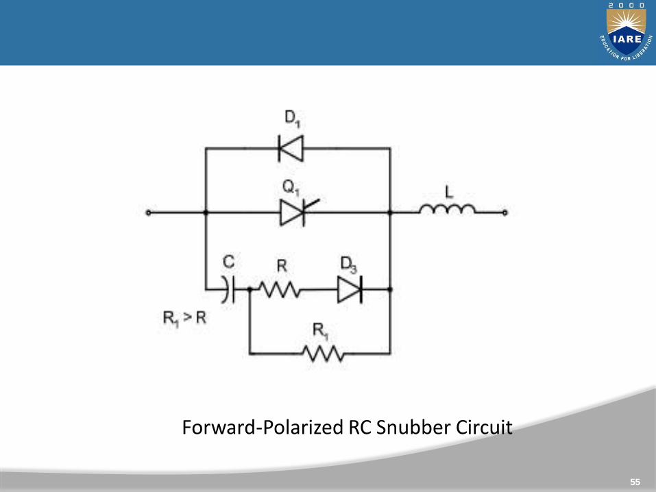
Forward-Polarized RC Snubber Circuit
Cont..
56
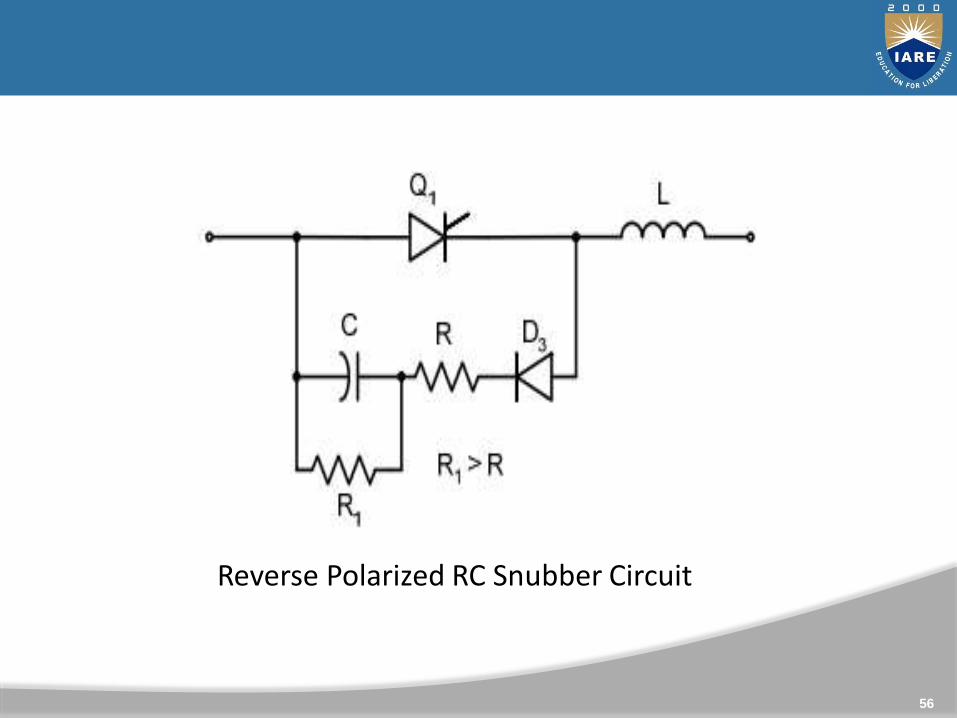
Reverse Polarized RC Snubber Circuit
57
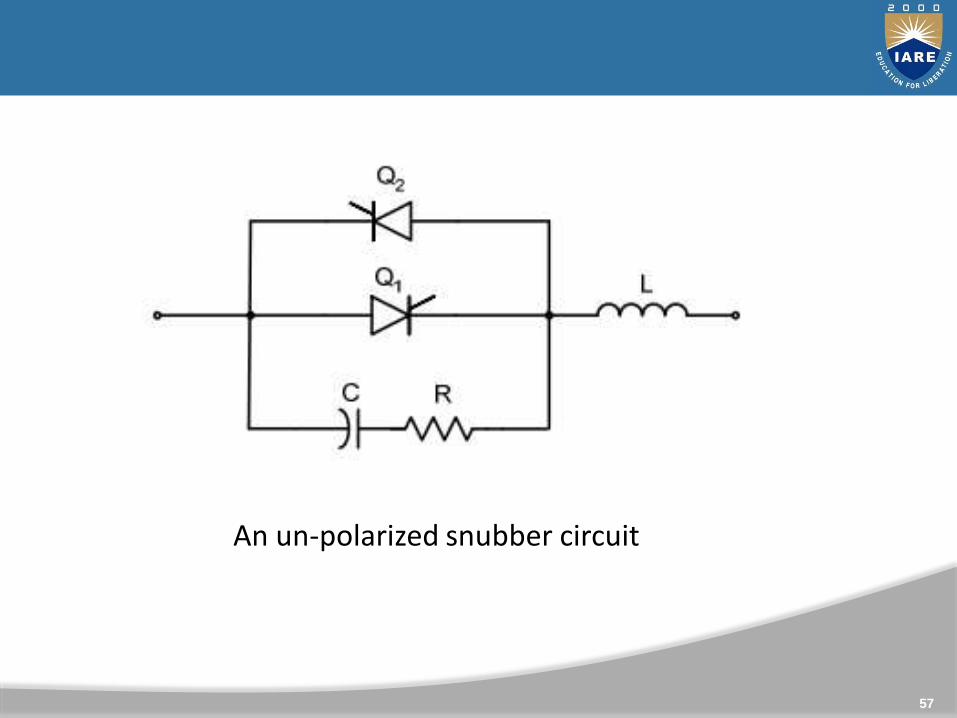
An un-polarized snubber circuit
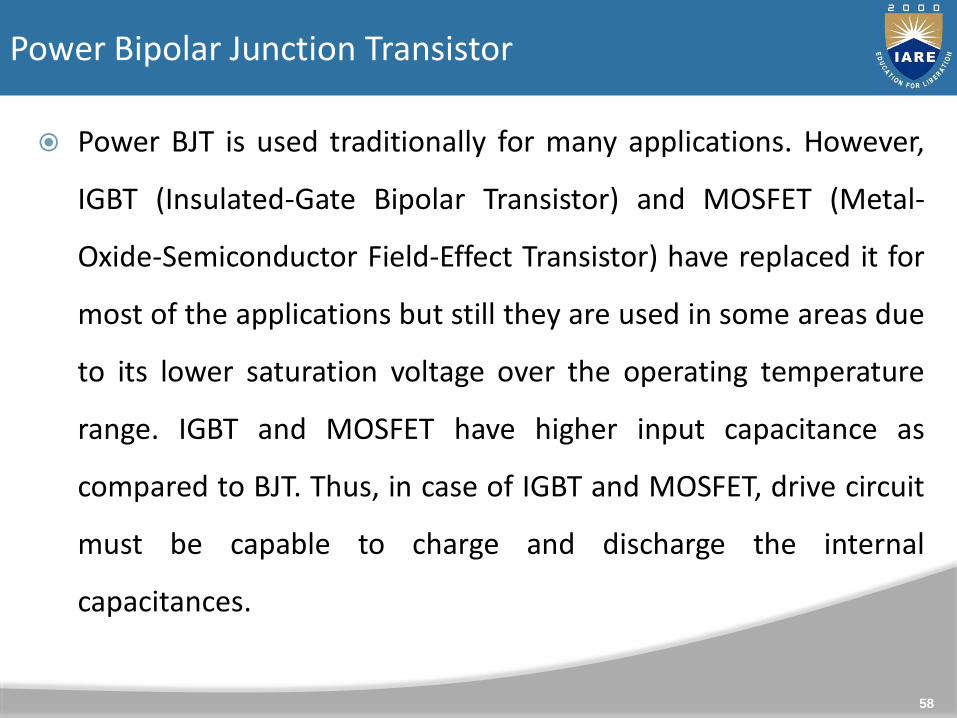
Power BJT is used traditionally for many applications. However,
IGBT (Insulated-Gate Bipolar Transistor) and MOSFET (Metal-
Oxide-Semiconductor Field-Effect Transistor) have replaced it for
most of the applications but still they are used in some areas due
to its lower saturation voltage over the operating temperature
range. IGBT and MOSFET have higher input capacitance as
compared to BJT. Thus, in case of IGBT and MOSFET, drive circuit
must be capable to charge and discharge the internal
capacitances.
58
Power Bipolar Junction Transistor
59
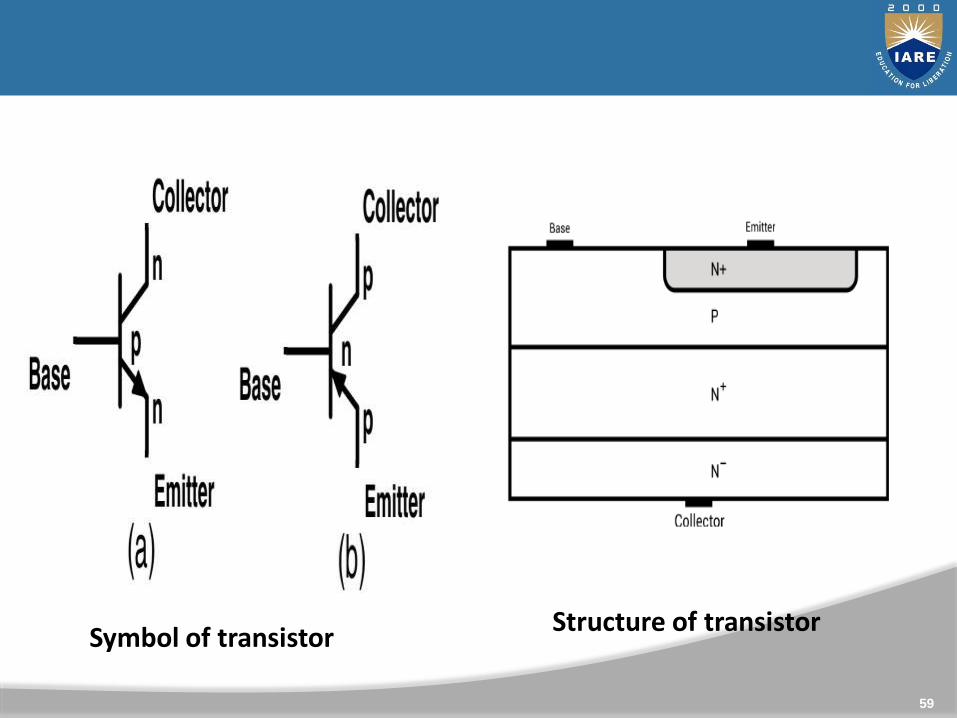
Symbol of transistorStructure of transistor
Cont..
60
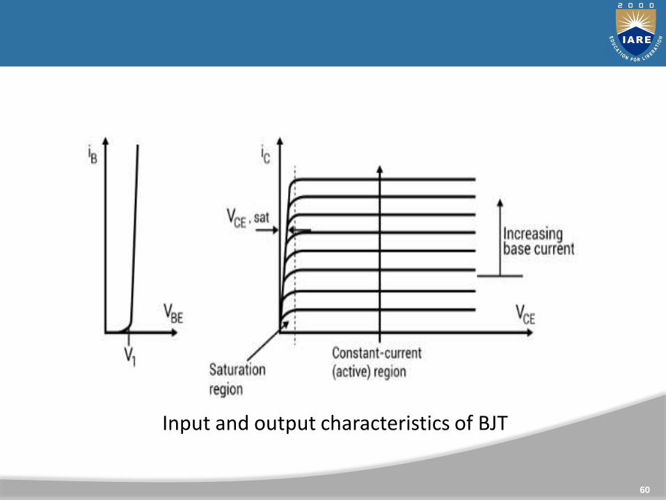
Input and output characteristics of BJT
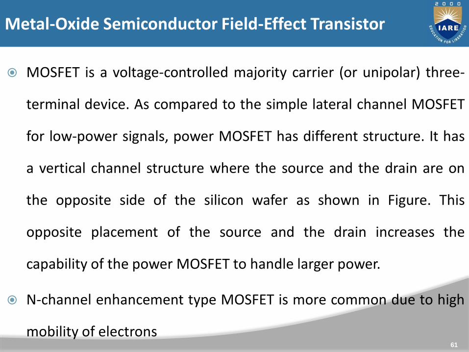
MOSFET is a voltage-controlled majority carrier (or unipolar) three-
terminal device. As compared to the simple lateral channel MOSFET
for low-power signals, power MOSFET has different structure. It has
a vertical channel structure where the source and the drain are on
the opposite side of the silicon wafer as shown in Figure. This
opposite placement of the source and the drain increases the
capability of the power MOSFET to handle larger power.
N-channel enhancement type MOSFET is more common due to high
mobility of electrons61
Metal-Oxide Semiconductor Field-Effect Transistor
62
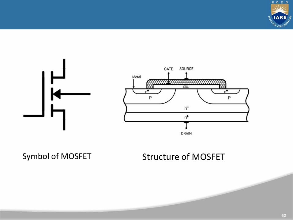
Symbol of MOSFET Structure of MOSFET
Cont..
63
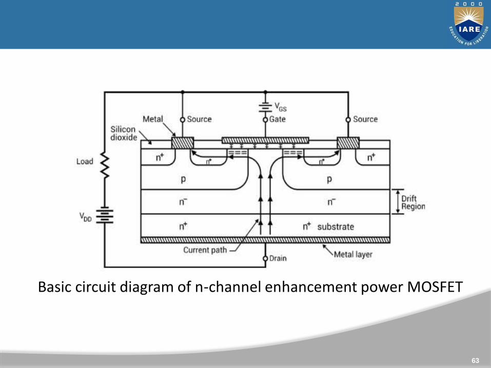
Basic circuit diagram of n-channel enhancement power MOSFET
Cont..
64
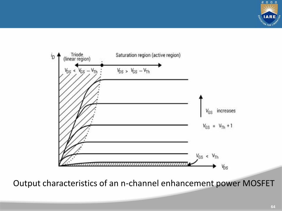
Output characteristics of an n-channel enhancement power MOSFET
Cont..
65
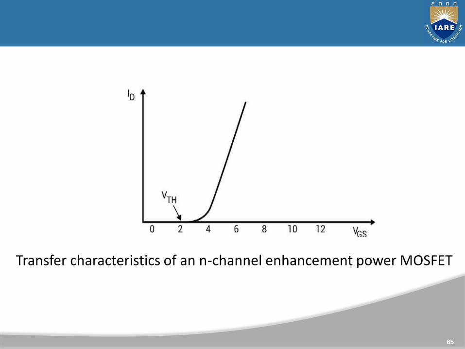
Transfer characteristics of an n-channel enhancement power MOSFET

IGBT combines the physics of both BJT and power MOSFET to
gain the advantages of both worlds. It is controlled by the gate
voltage. It has the high input impedance like a power MOSFET
and has low on-state power loss as in case of BJT. There is no
even secondary breakdown and not have long switching time as
in case of BJT. It has better conduction characteristics as
compared to MOSFET due to bipolar nature.
66
Insulated-Gate Bipolar Transistor (IGBT)
Cont..
67
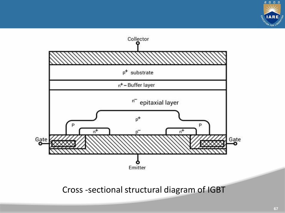
Cross -sectional structural diagram of IGBT
Cont..
68
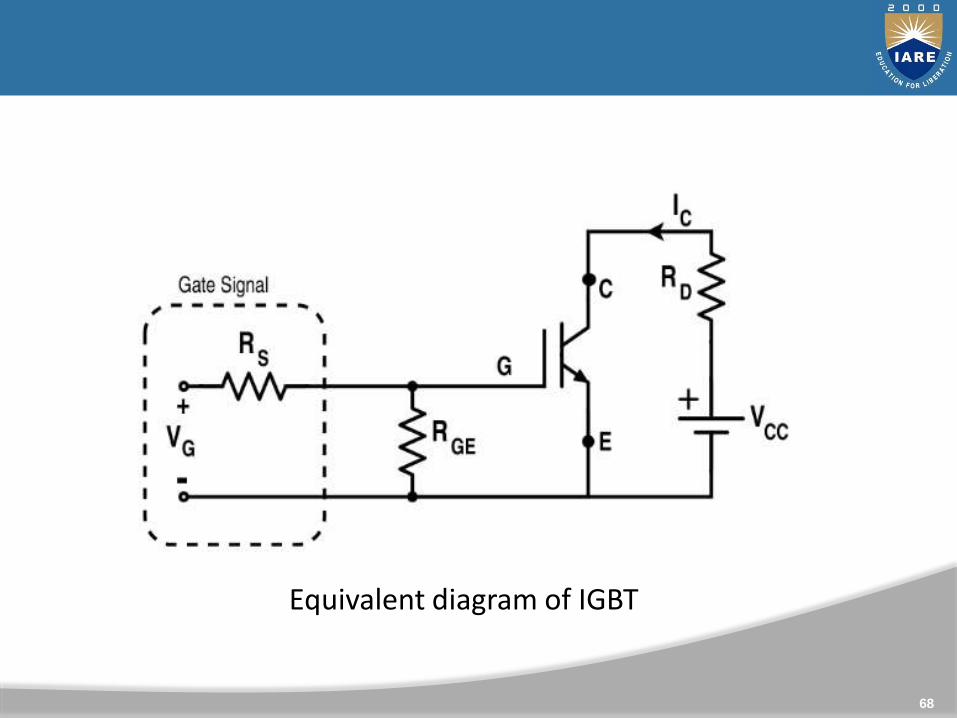
Equivalent diagram of IGBT

Cont..
69
Forward characteristics of IGBT Transfer characteristics of IGBT
GTO can be turned on with the positive gate current pulse and turned off
with the negative gate current pulse. Its capability to turn off is due to the
diversion of PNP collector current by the gate and thus breaking the
regenerative feedback effect.
Actually the design of GTO is made in such a way that the pnp current
gain of GTO is reduced. A highly doped n spot in the anode p layer form a
shorted emitter effect and ultimately decreases the current gain of GTO
for lower current regeneration and also the reverse voltage blocking
capability. This reduction in reverse blocking capability can be improved
by diffusing gold but this reduces the carrier lifetime. Moreover, it
requires a special protection.70
GTO (Gate Turn-off Thyristor)
Cont..
71
Gate Drive Circuit for GTOSymbol of GTO
Cont..
72
Switching characteristics for GTO
Peak Invese Voltage (VPIV)
The peak inverse voltage is defined as the maximum voltage which SCRcan safely withstand in its OFF state. The applied voltage should neverbe exceeded under any circumstances.
On State Voltage:
The voltage which appears across the SCR during its ON state is knownas its ON state Voltage. The maximum value of voltage which canappear across the SCR during its conducting state is called its maximumon state voltage. Usually it will be 1V to 4V.
Finger Voltage:
The minimum voltage, which is required between the anode andcathode of an SCR to trigger it to conduction mode, is called its fingervoltage.
73
SCR Specifications and Ratings:
Cont..
Rate of Rise of Voltage (dV/dt)
The rate at which the voltage across the device rises ( forforward condition) without triggering the device, is known as itsrate of rise of voltage.
Voltage Safety Factor:
The normal operating voltage of the SCR is kept well below itspeak inverse voltage(VPIV) to avoid puncture of SCR due touncertain conditions. The operating voltage and peak inversevoltage are related by voltage safety factor Vf
Vf = Peak inverse voltage / ( 2 x RMS value of input voltage)
74
Cont..
Maximum average ON state current ( Imac):
This is the average value of maximum continuous sinusoidal ON statecurrent with conduction angle 180deg, at frequency 40 to 60Hz, whichshould not be exceeded even with intensive cooling.
Maximum rms ON-state current: (Imrc)
It is the rms value of the maximum continuous sinusoidal ON statecurrent at the frequency 40 to 60 Hz and conduction angle 180deg,which should not be exceeded even with intensive cooling.
Maximum surge - ON state Current (Imsc)
It is the maximum admissible peak value of a sinusoidal half cycle oftem milliseconds duration at a frequency of 50Hz.
75
Cont.. Latching Current (II)
It is the minimum current, which is required to latch the device from its OFF state to its ON state. In other words, it is the minimum current required to trigger the device.
Holding Current (IH)
It is the minimum current required to hold the SCR conducting. In other words, It is the minimum current, below which the device stops conducting and returns to its OFF state.
Gate Current:
The current which is applied to the gate of the device for control purposes is known as gate current.
76
Cont..
Minimum Gate Current:
The minimum current required at the gate for triggering the device.
Maximum Gate Current:
The maximum current which can be applied to device safely. Current higher than this will damage the gate terminal.
Gate Power Loss:
The mean power loss, which occurs due to flow of gate current between the gate and the main terminals.
77
The term PCR or Phase controlled rectifier is a one type of
rectifier circuit in which the diodes are switched by Thyristors or
SCRs (Silicon Controlled Rectifiers). Whereas the diodes offer no
control over the o/p voltage, the Thyristors can be used to differ
the output voltage by adjusting the firing angle or delay. A phase
control Thyristor is activated by applying a short pulse to its gate
terminal and it is deactivated due to line communication or
natural. In case of heavy inductive load, it is deactivated by firing
another Thyristor of the rectifier during the negative half cycle of
i/p voltage.79
Phase control technique
80
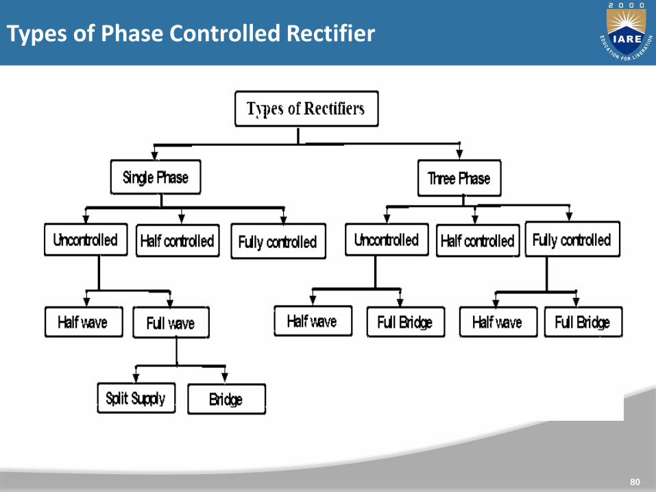
Types of Phase Controlled Rectifier
81
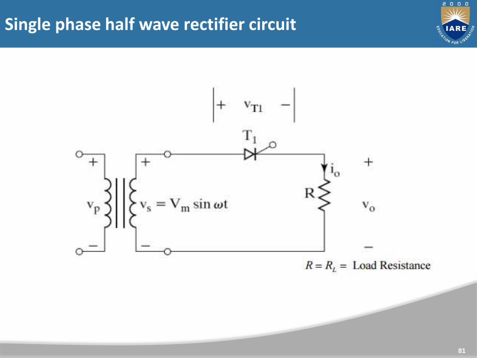
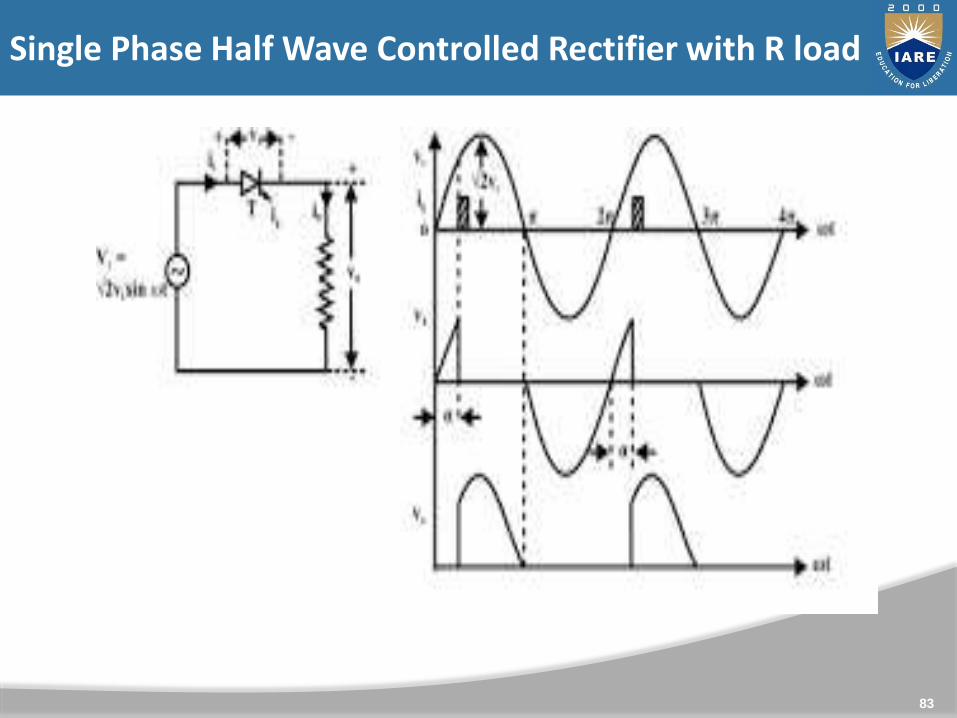
Single phase half wave rectifier circuit
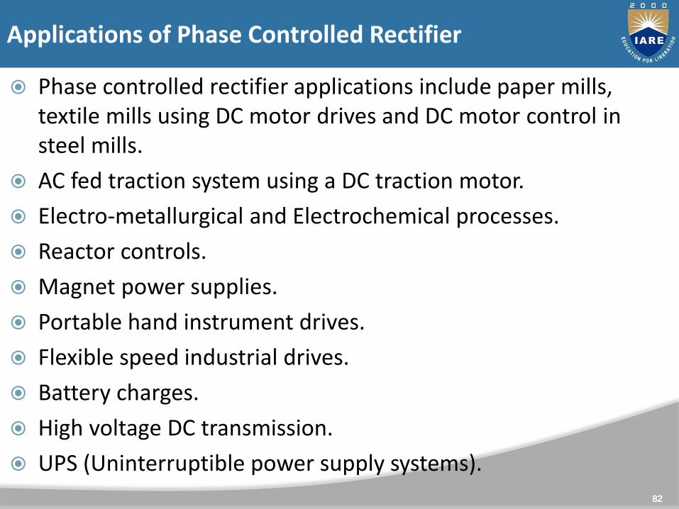
Phase controlled rectifier applications include paper mills, textile mills using DC motor drives and DC motor control in steel mills.
AC fed traction system using a DC traction motor.
Electro-metallurgical and Electrochemical processes.
Reactor controls.
Magnet power supplies.
Portable hand instrument drives.
Flexible speed industrial drives.
Battery charges.
High voltage DC transmission.
UPS (Uninterruptible power supply systems).
82
Applications of Phase Controlled Rectifier
83
Single Phase Half Wave Controlled Rectifier with R load
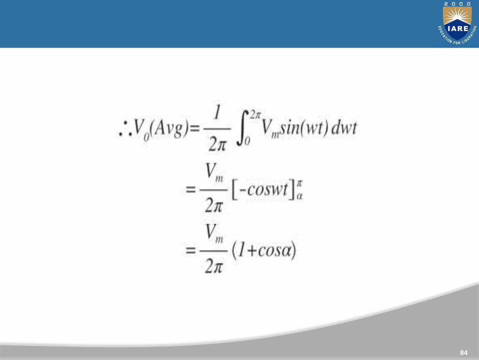
Cont..
84
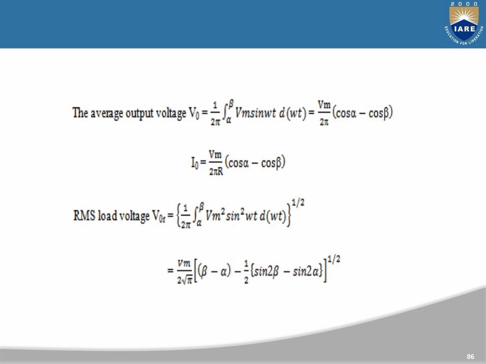
85
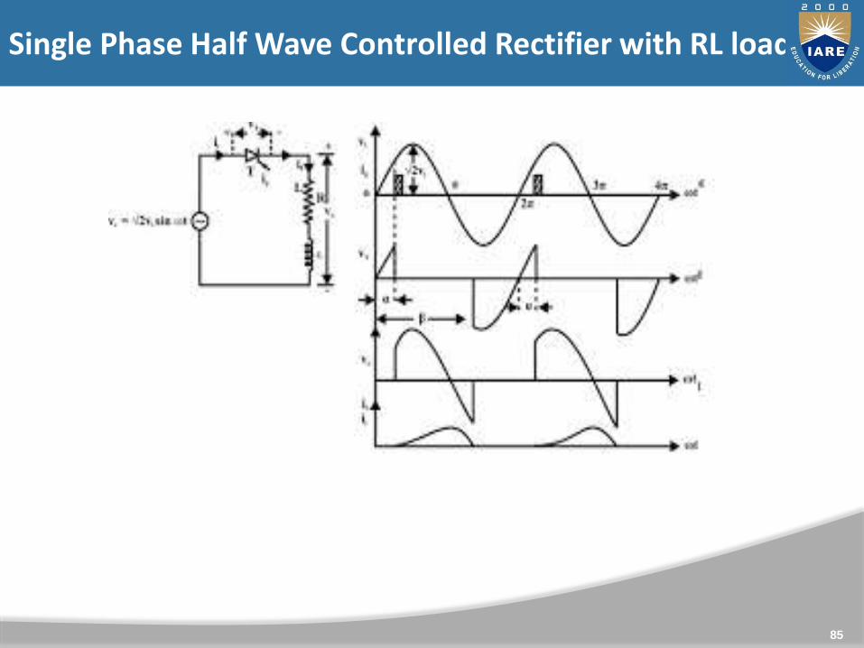
Single Phase Half Wave Controlled Rectifier with RL load
Cont..
86
87
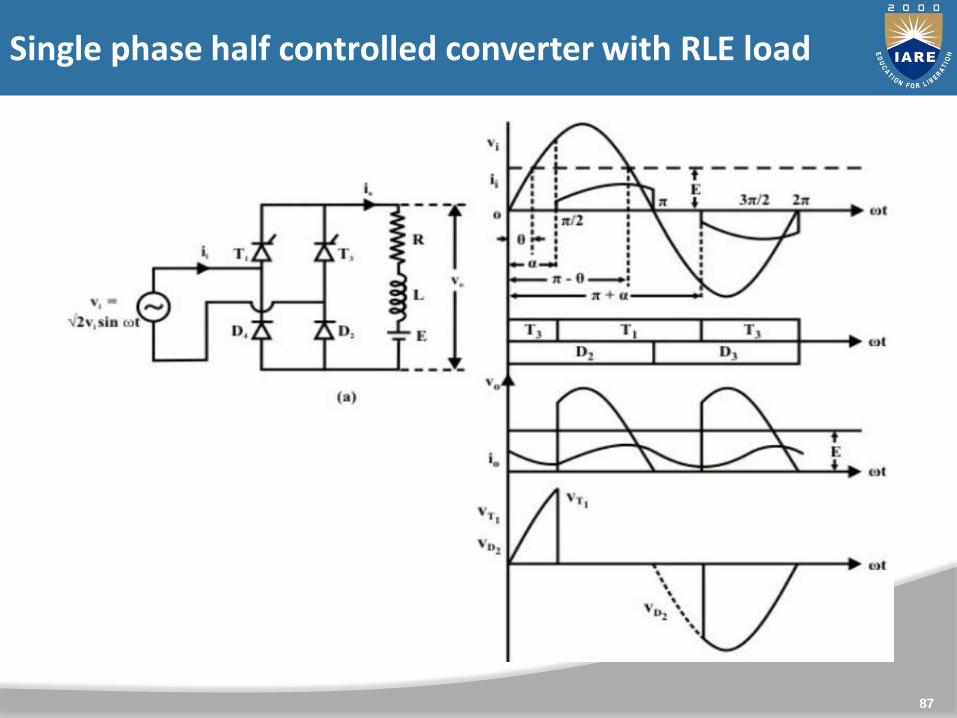
Single phase half controlled converter with RLE load
Cont..
The diode D2 and D4 conducts for the positive and negative half
cycle of the input voltage waveform respectively. On the other
hand T1 starts conduction when it is fired in the positive half cycle
of the input voltage waveform and continuous conduction till T3 is
fired in the negative half cycle. Fig. shows the circuit diagram and
the waveforms of a single phase half controlled converter
supplying an R – L – E load.
88
Cont..
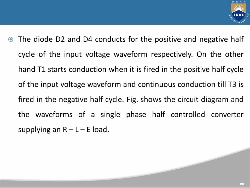
89
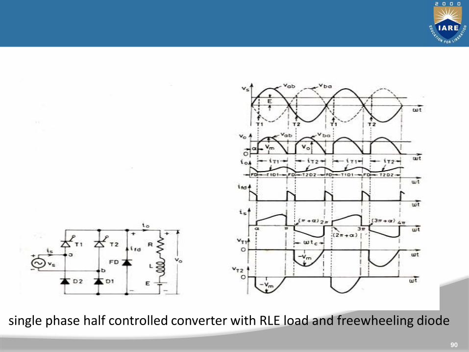
Cont..
90
single phase half controlled converter with RLE load and freewheeling diode
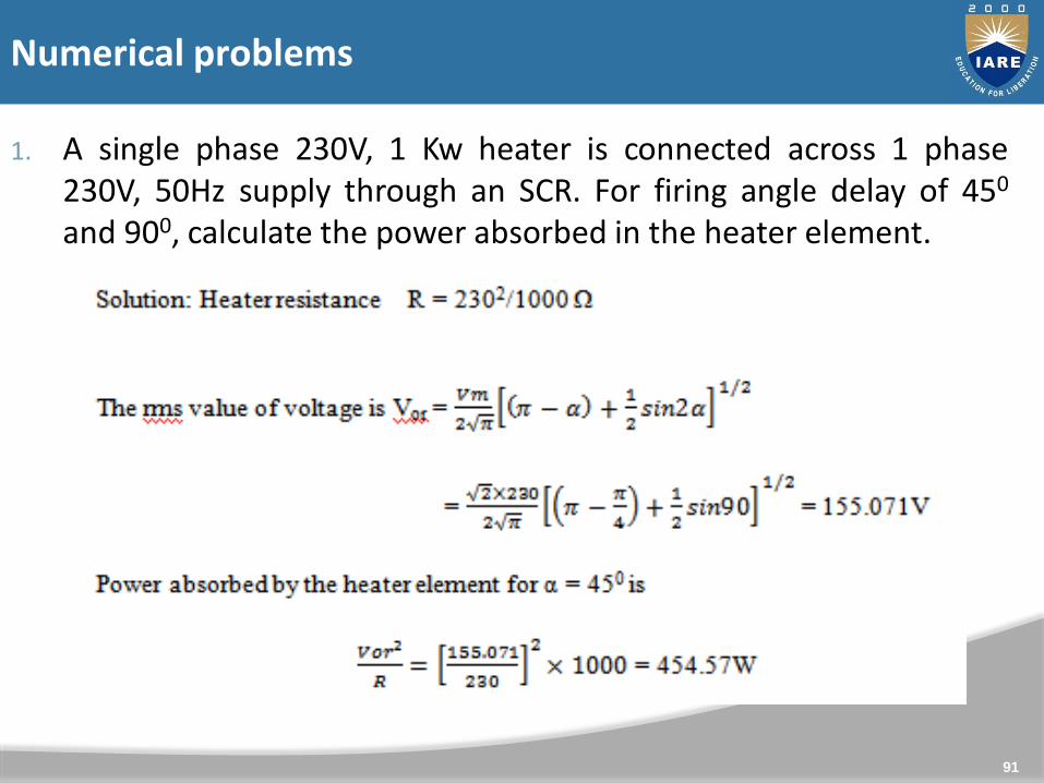
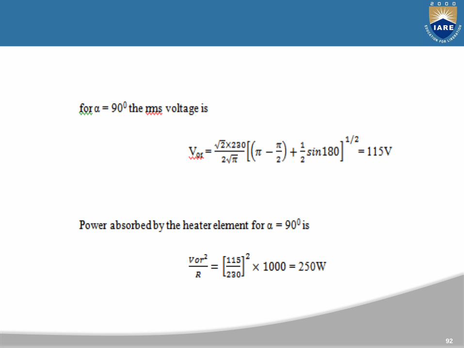
1. A single phase 230V, 1 Kw heater is connected across 1 phase230V, 50Hz supply through an SCR. For firing angle delay of 450
and 900, calculate the power absorbed in the heater element.
91
Numerical problems
Cont..
92
2. A resistive load of 10Ω is connected through a half-wave controlledrectifier circuit to 220V, 50 Hz, single phase source. Calculate thepower delivered to the load for a firing angle of 60ᵒ. Find also thevalue of input power factor
3. A single phase semi converter delivers to RLE load with R=5Ω, L =10mH and E = 80V. The source voltage is 230V, 50Hz. Forcontinuous conduction, Find the average value of output currentfor firing angle = 50o.
93
94
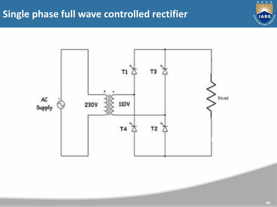
Single phase full wave controlled rectifier
Cont..
95
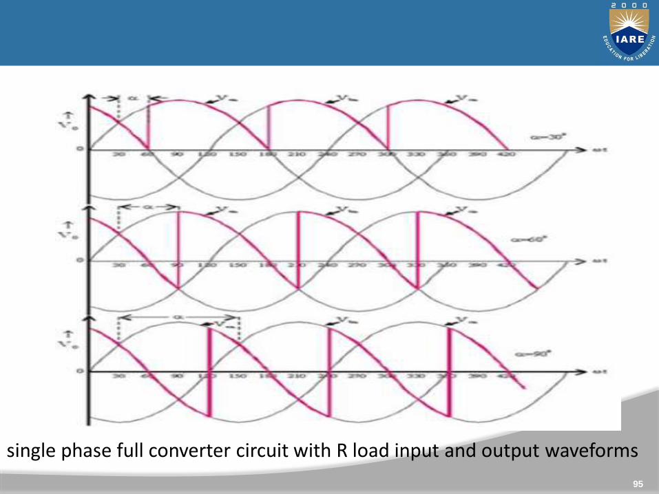
single phase full converter circuit with R load input and output waveforms
96
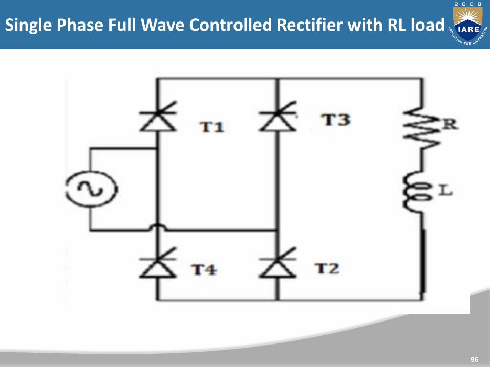
Single Phase Full Wave Controlled Rectifier with RL load
Cont..
97
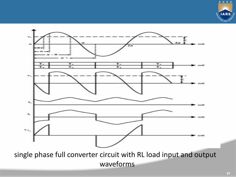
single phase full converter circuit with RL load input and output waveforms
98
Single phase fully controlled converters with RLE load
Cont..
In positive half-cycle of the input, Thyristors T1 and T2 are
forward biased while T3 and T4 are reverse biased. Thyristors
T1 and T2 are triggered simultaneously at some firing angle in
the positive half cycle, and T3 and T4 are triggered in the
negative half cycle.
The load current starts flowing through them when they are
in conduction state. The load for this converter can be RL or
RLE depending on the application.
99
Cont..
100
single phase full converter circuit with RLE load input and output waveforms
101
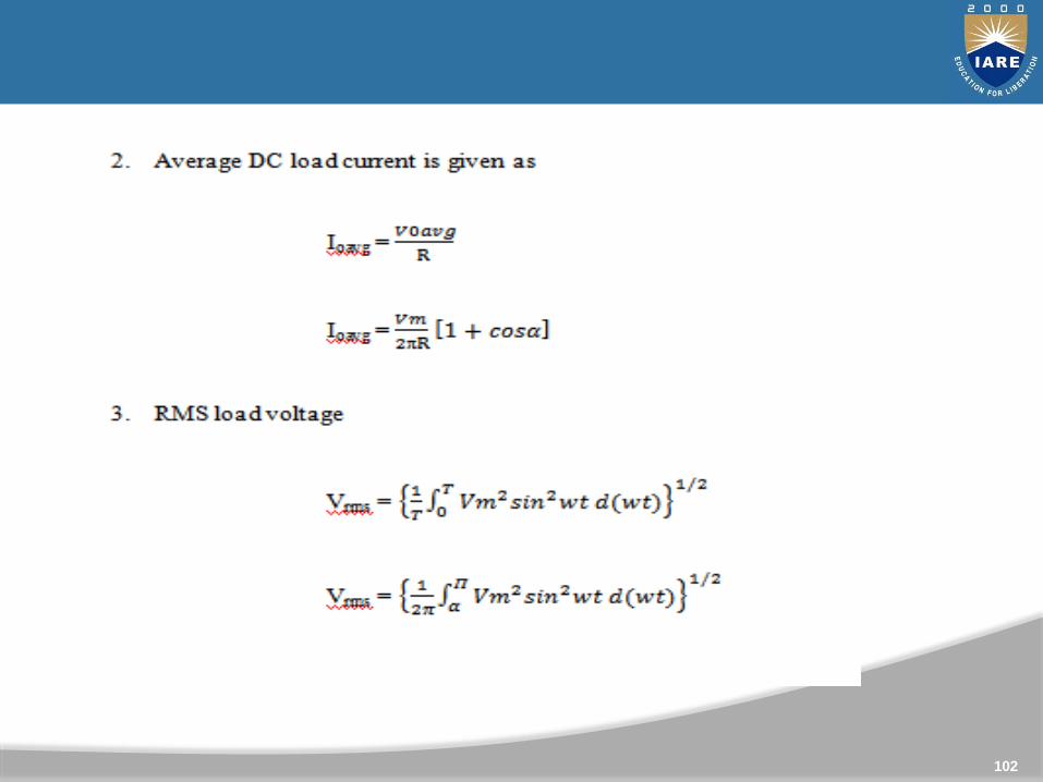
single phase half wave converter
Cont..
102
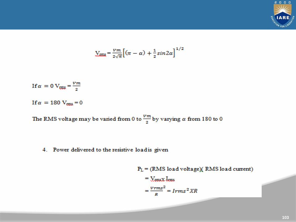
Cont..
103
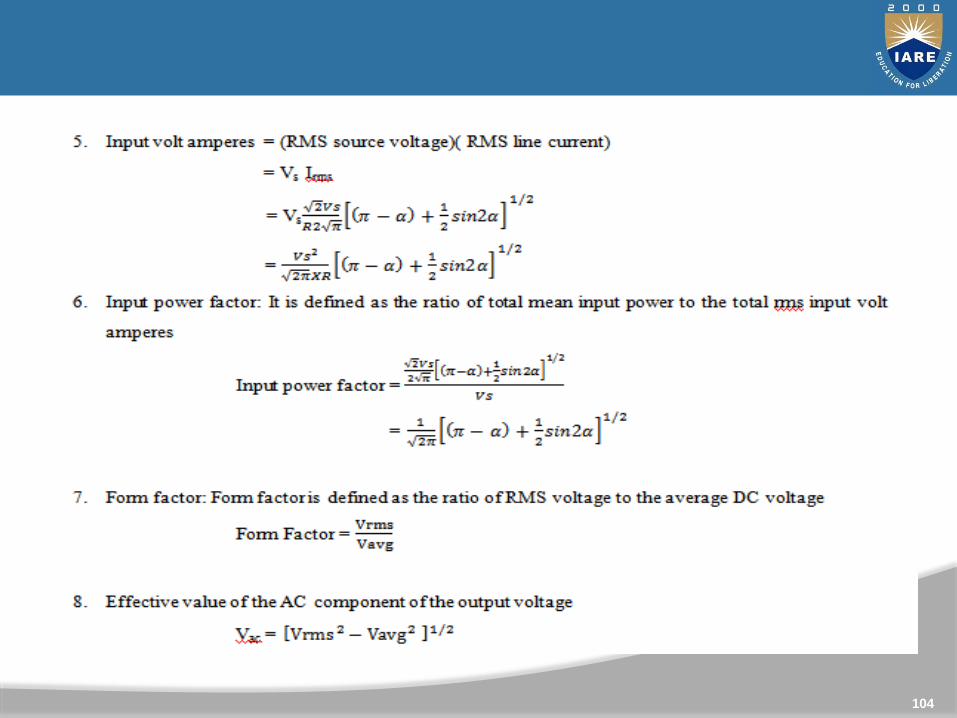
Cont..
104
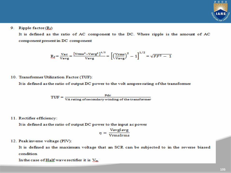
Cont..
105
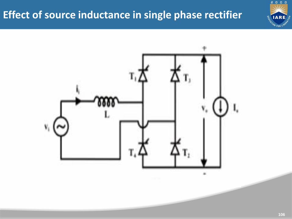
106
Effect of source inductance in single phase rectifier
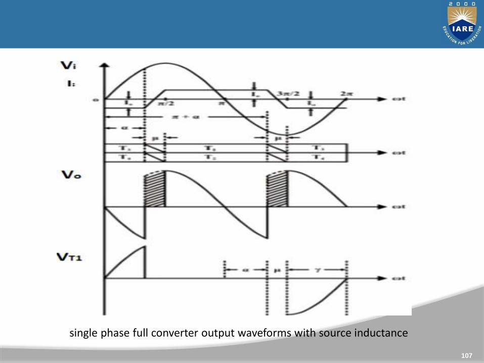
Cont..
107
single phase full converter output waveforms with source inductance
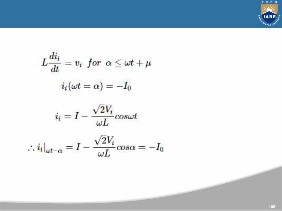
Cont..
108
Cont..
109
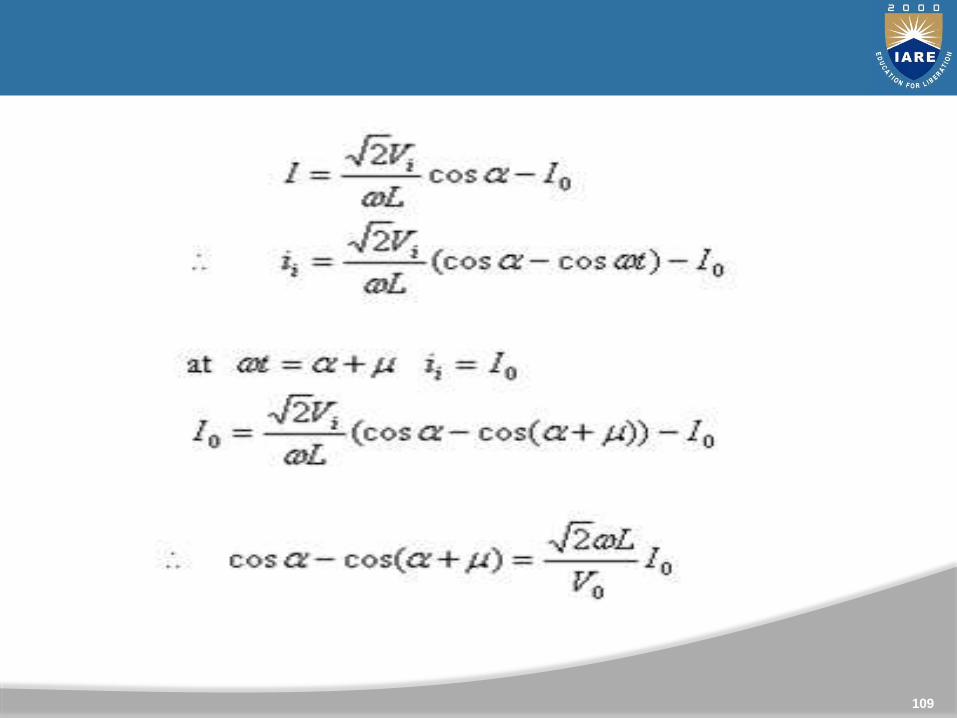
Cont..
110
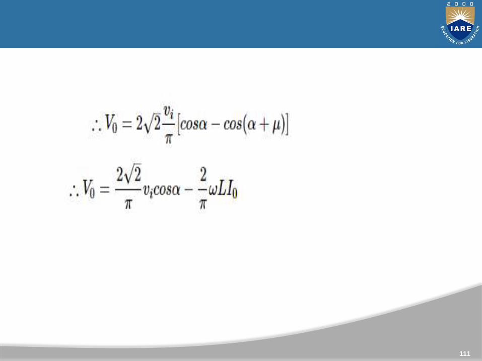
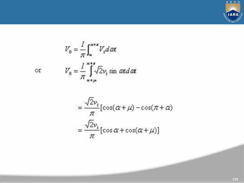
Cont..
111
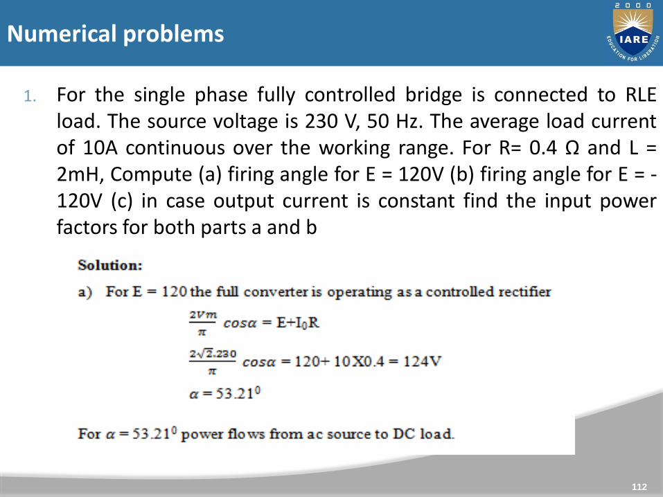
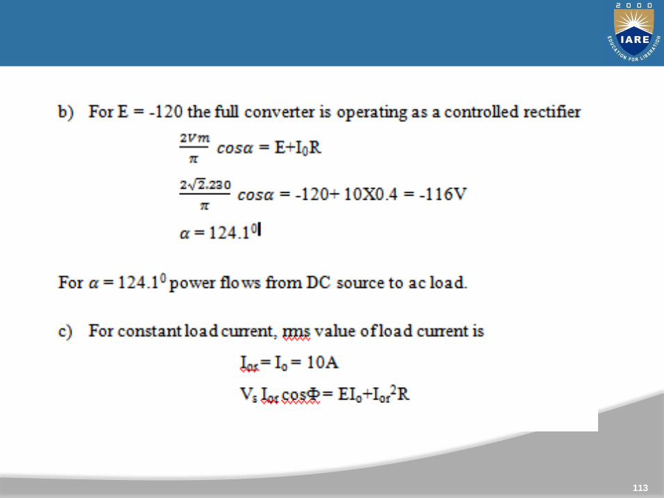
1. For the single phase fully controlled bridge is connected to RLEload. The source voltage is 230 V, 50 Hz. The average load currentof 10A continuous over the working range. For R= 0.4 Ω and L =2mH, Compute (a) firing angle for E = 120V (b) firing angle for E = -120V (c) in case output current is constant find the input powerfactors for both parts a and b
112
Numerical problems
Cont..
113
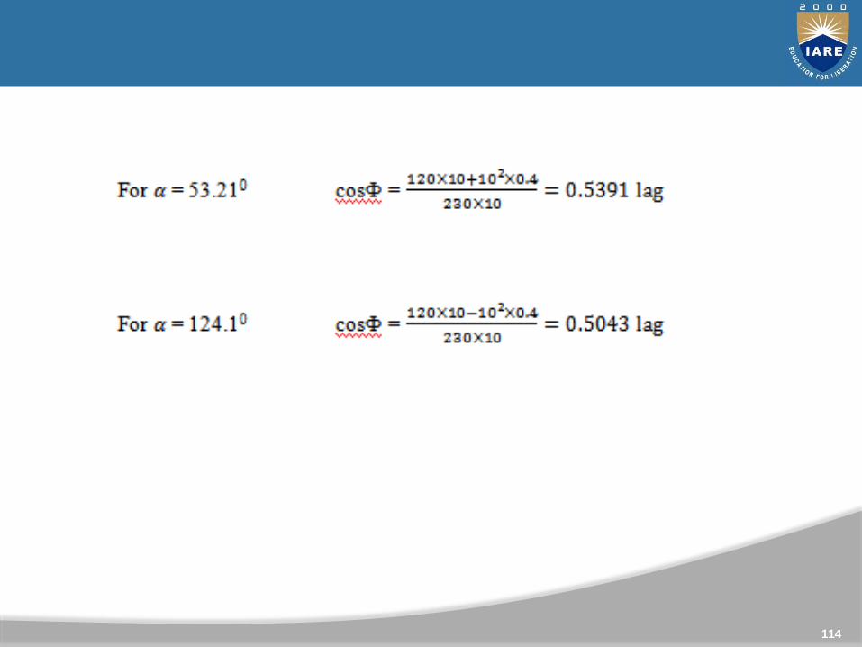
Cont..
114
2. A single phase two pulse converter feeds power to RLE load with R=
6Ω, L= 6mH, E= 60V, AC source voltage is 230V, 50Hz for continuous
condition. Find the average value of load current for a firing angle of
50ᵒ. In case one of the 4 SCRs gets open circuited. Find the new value
of average load current assuming the output current as continuous.
3. For the single phase fully controlled bridge converter having load of
‘R’, determine the average output voltage, rms output voltage and
input power factor if the supply is 230V, 50 Hz, single phase AC and
the firing angle is 60 degrees
115
116
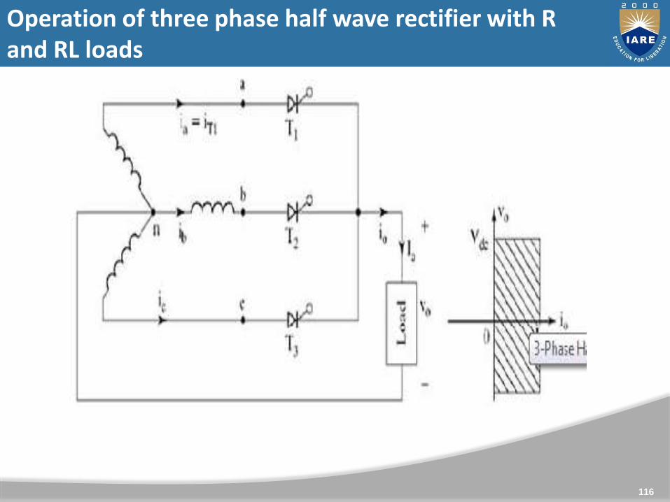
Operation of three phase half wave rectifier with R and RL loads
Cont..
117
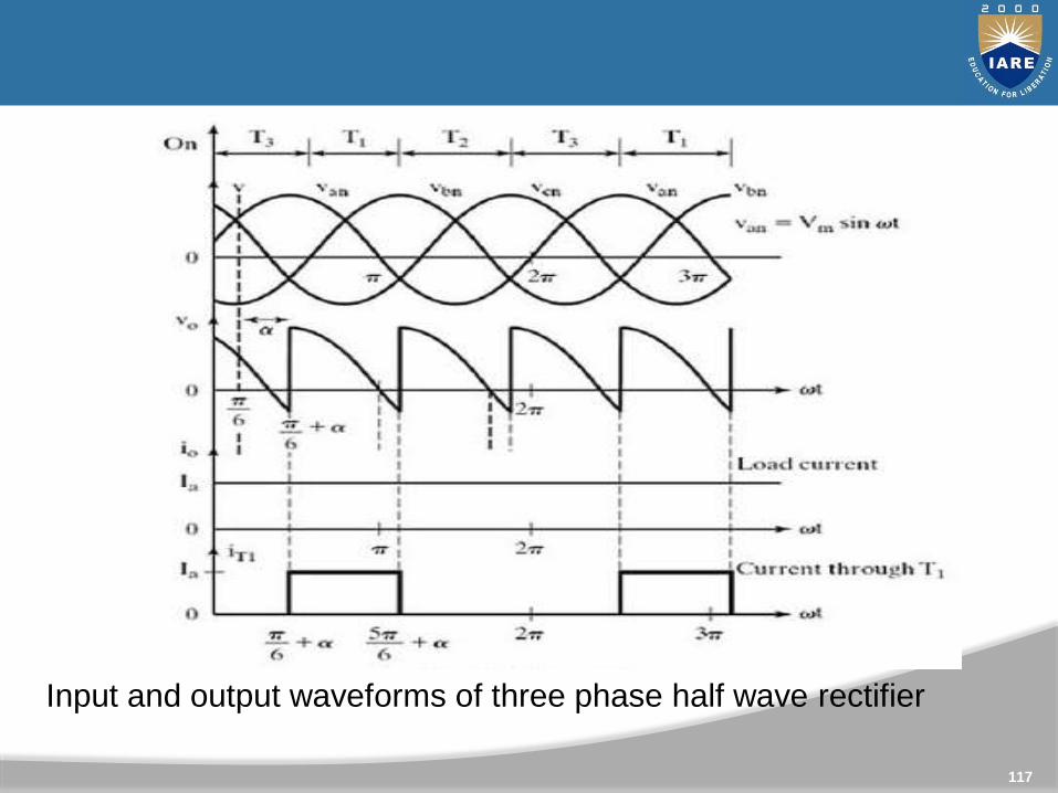
Input and output waveforms of three phase half wave rectifier
Cont..
118
119
circuit diagram three phase half controlled rectifier
Operation of three phase half controlled rectifier with R and RL loads
Cont..
120
Input and output waveforms of three phase half controlled rectifier with R load
Cont..
121
Cont..
122
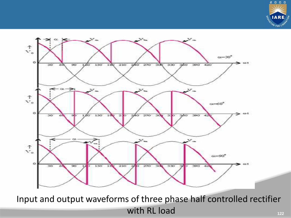
Input and output waveforms of three phase half controlled rectifierwith RL load
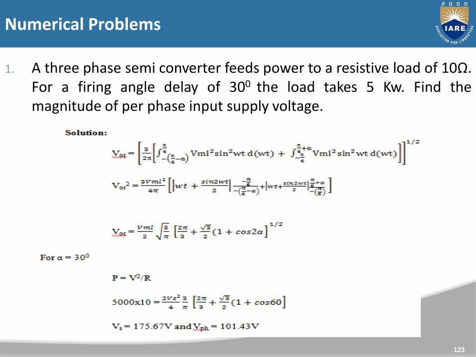
1. A three phase semi converter feeds power to a resistive load of 10Ω.For a firing angle delay of 300 the load takes 5 Kw. Find themagnitude of per phase input supply voltage.
123
Numerical Problems
2. A three-phase half-wave controlled rectifier has a supply of
200V/phase. Determine the average load voltage for firing angle of
0o, 30oand 60o assuming a thyristor volt drop of 1.5V and
continuous load current
3 A three phase half wave converter is supplying a load with a
continuous constant current of 50A over a firing angle from 0o to
600. What will be the power dissipated by the load at these limiting
values of firing angle. The supply voltage is 415V (line).
124
125
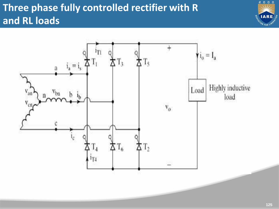
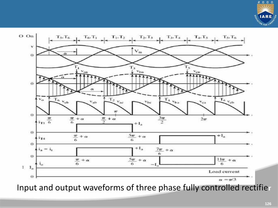
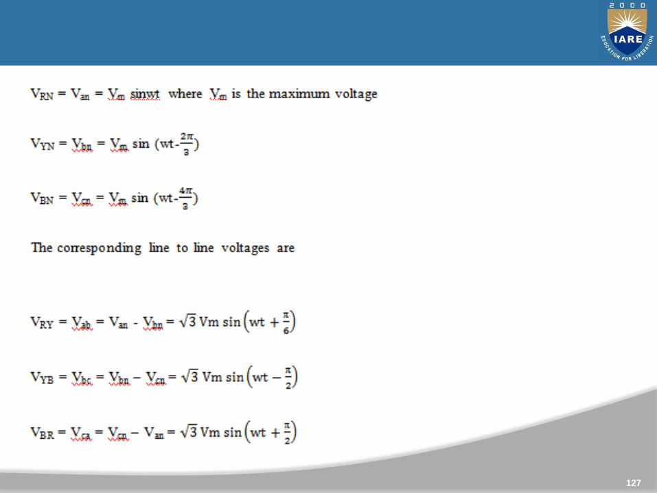
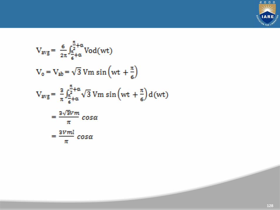
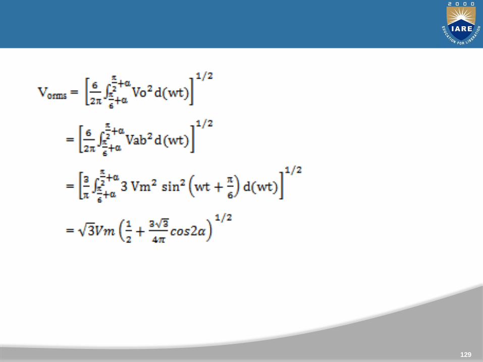
Three phase fully controlled rectifier with R and RL loads
Cont..
126
Input and output waveforms of three phase fully controlled rectifier
Cont..
127
Cont..
128
Cont..
129
130
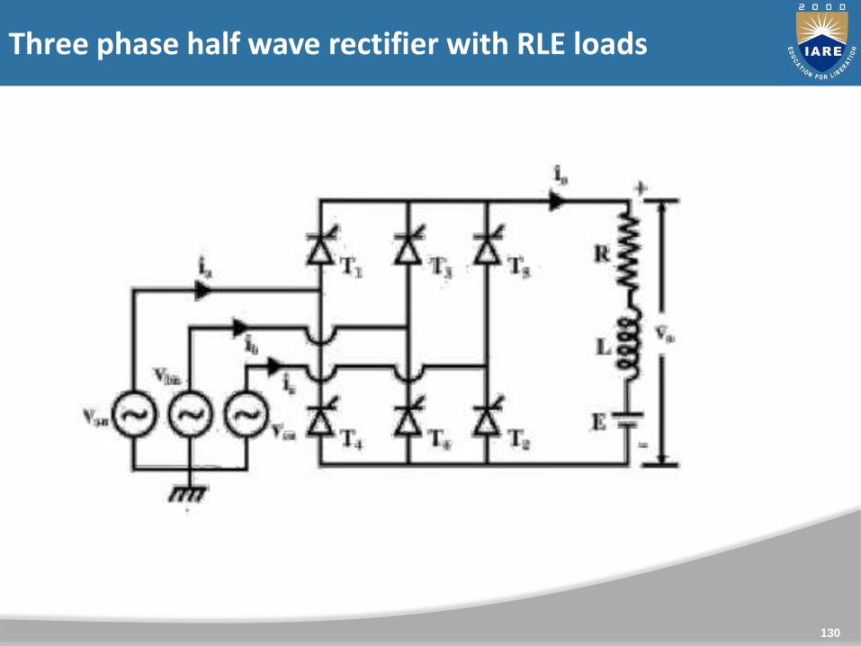
Three phase half wave rectifier with RLE loads
Cont..
131
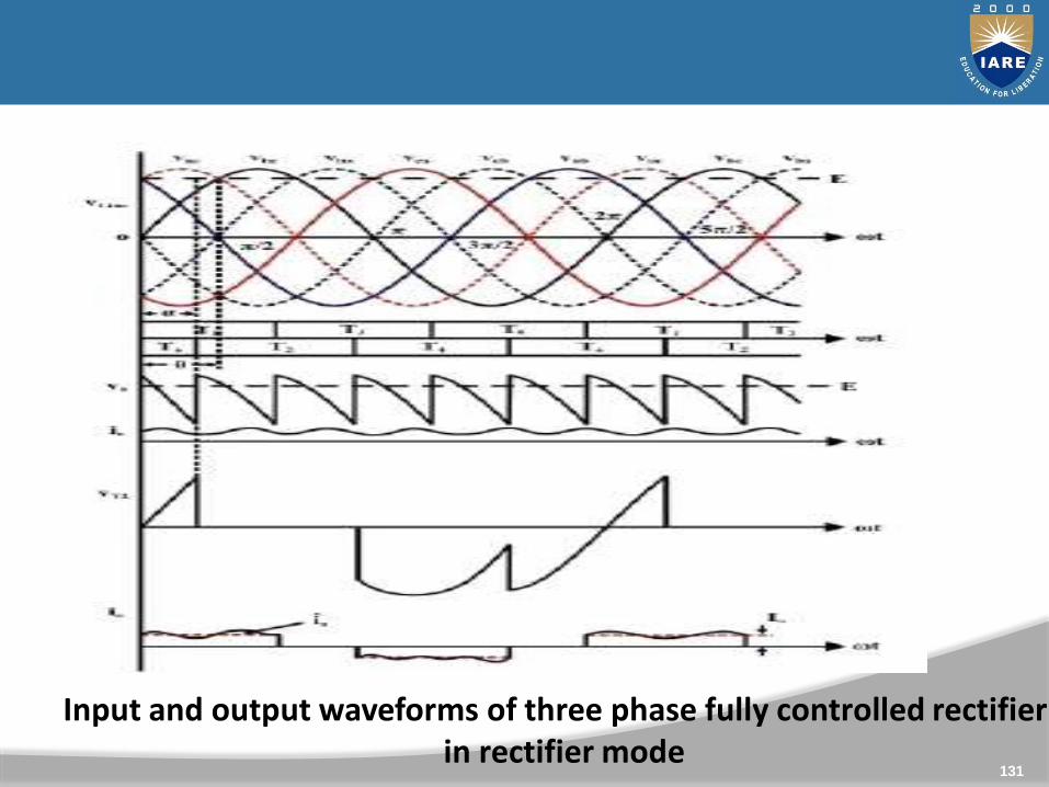
Input and output waveforms of three phase fully controlled rectifier in rectifier mode
Cont..
132
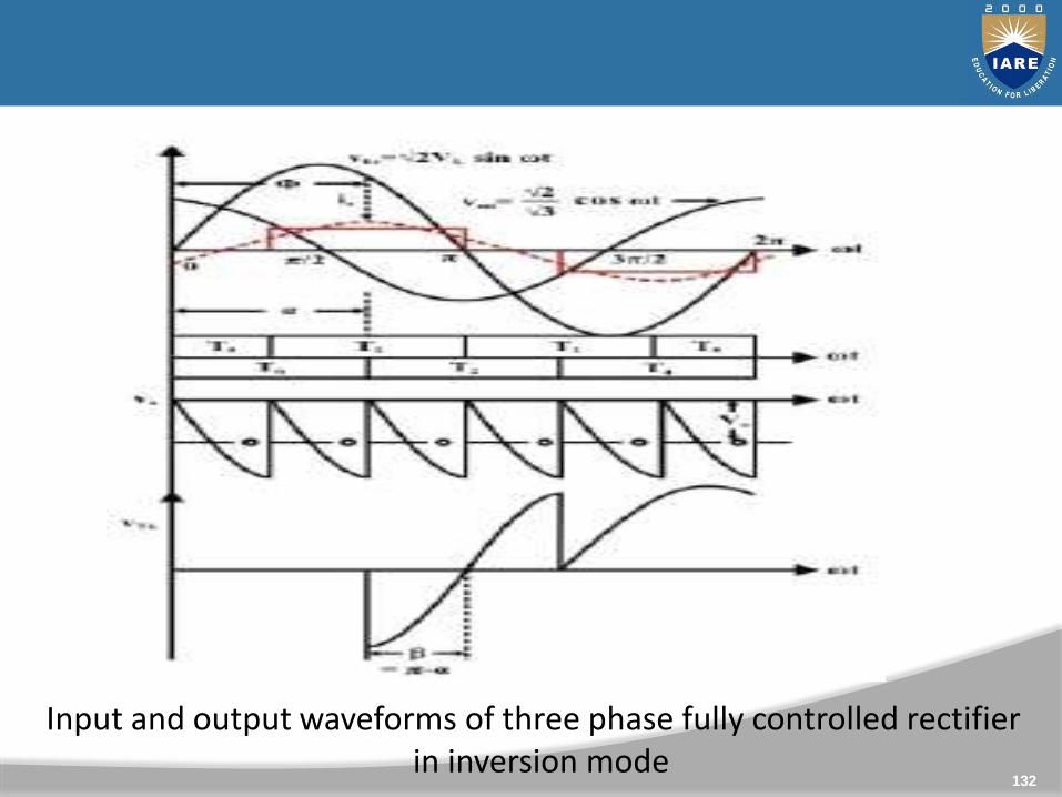
Input and output waveforms of three phase fully controlled rectifier in inversion mode
133
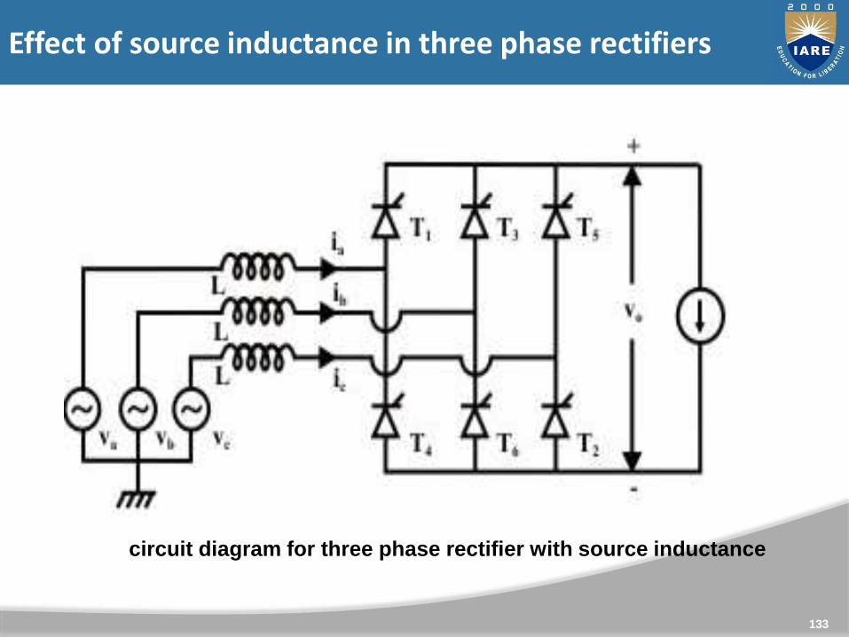
circuit diagram for three phase rectifier with source inductance
Effect of source inductance in three phase rectifiers
Cont..
134
waveforms for three phase rectifier with source inductance
Cont..
135
Cont..
136
Cont..
137
Dual converter, the name itself says two converters. It is really an
electronic converter or circuit which comprises of two
converters. One will perform as rectifier and the other will
perform as inverter. Therefore, we can say that double processes
will occur at a moment. Here, two full converters are arranged in
anti-parallel pattern and linked to the same dc load. These
converters can provide four quadrant operations.
138
Dual converters
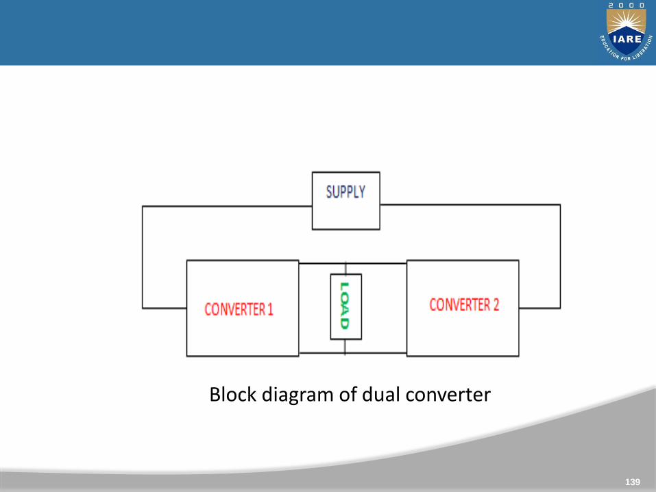
Cont..
139
Block diagram of dual converter
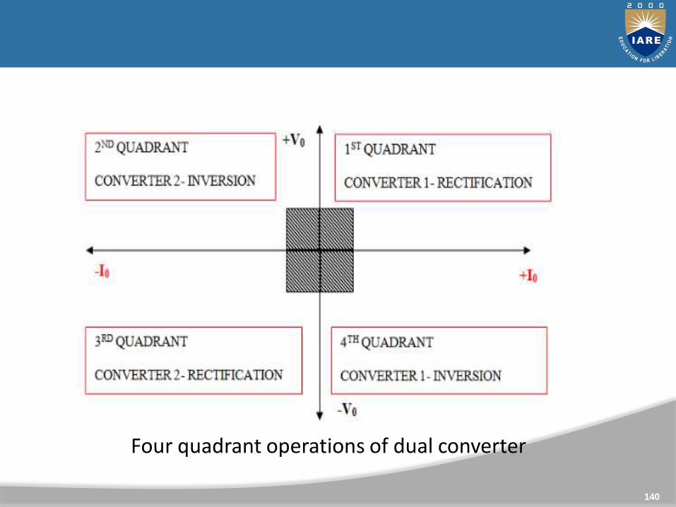
Cont..
140
Four quadrant operations of dual converter
Cont..
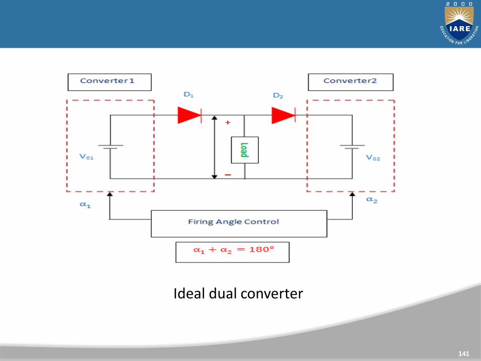
141
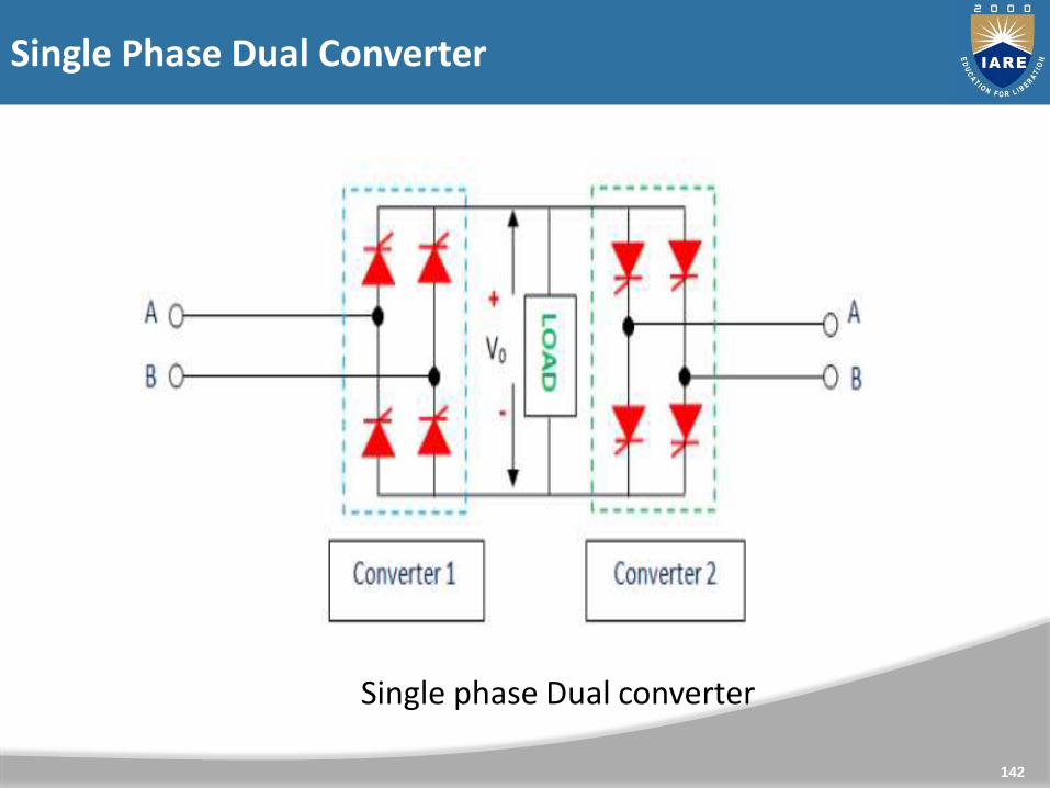
Ideal dual converter
142
Single phase Dual converter
Single Phase Dual Converter
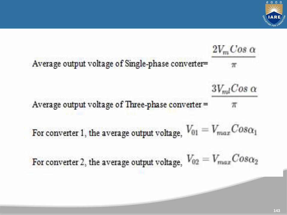
Cont..
143
Cont..
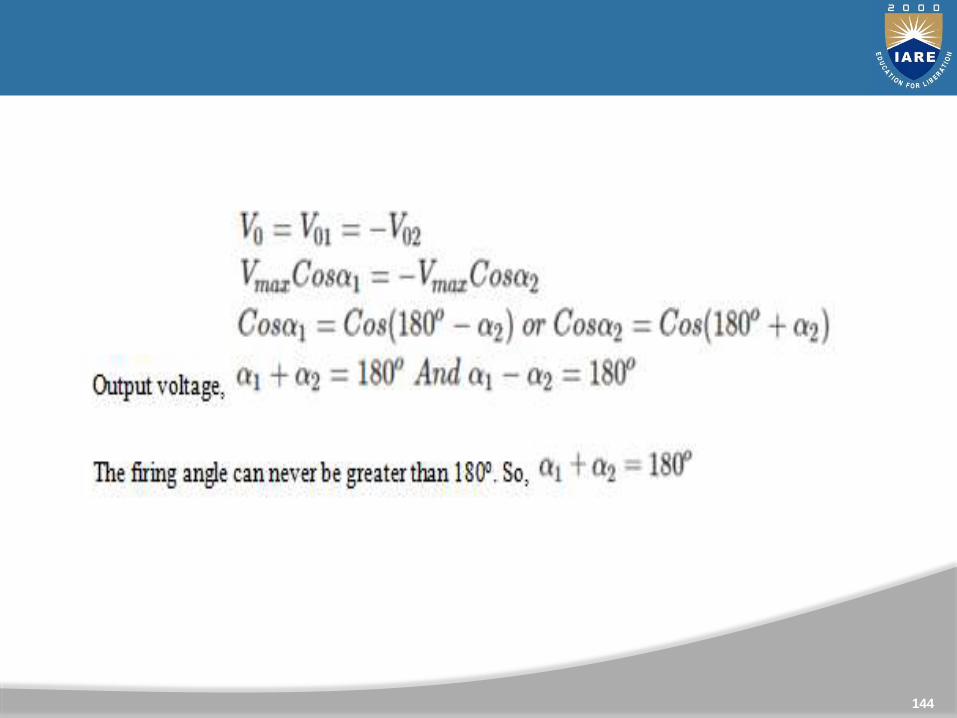
144
Cont..
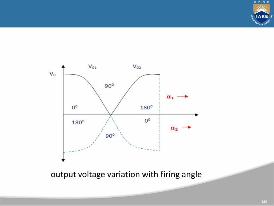
145
output voltage variation with firing angle
146
Three phase dual converter
Three Phase Dual Converter
Direction and Speed control of DC motors.
Applicable wherever the reversible DC is required.
Industrial variable speed DC drives.
147
Application of Dual Converter
AC voltage controllers (ac line voltage controllers) are employed to
vary the RMS value of the alternating voltage applied to a load
circuit by introducing Thyristors between the load and a constant
voltage ac source. The RMS value of alternating voltage applied to
a load circuit is controlled by controlling the triggering angle of the
Thyristors in the AC Voltage Controller circuits.
Control strategies: There are two different types of thyristorcontrol used in practice to control the ac power flow
On-Off control
Phase control
149
AC voltage controllers
Cont..
Phase control
In phase control the Thyristors are used as switches to connect
the load circuit to the input ac supply, for a part of every input
cycle. That is the ac supply voltage is chopped using Thyristors
during a part of each input cycle.
The thyristor switch is turned on for a part of every half cycle, so
that input supply voltage appears across the load and then
turned off during the remaining part of input half cycle to
disconnect the ac supply from the load.
150
Cont..
Applications of ac voltage controllers
Lighting / Illumination control in ac power circuits.
Induction heating.
Industrial heating & Domestic heating.
Transformers tap changing (on load transformer tap changing).
Speed control of induction motors (single phase and poly phase ac
induction motor control).
AC magnet controls.
151
152
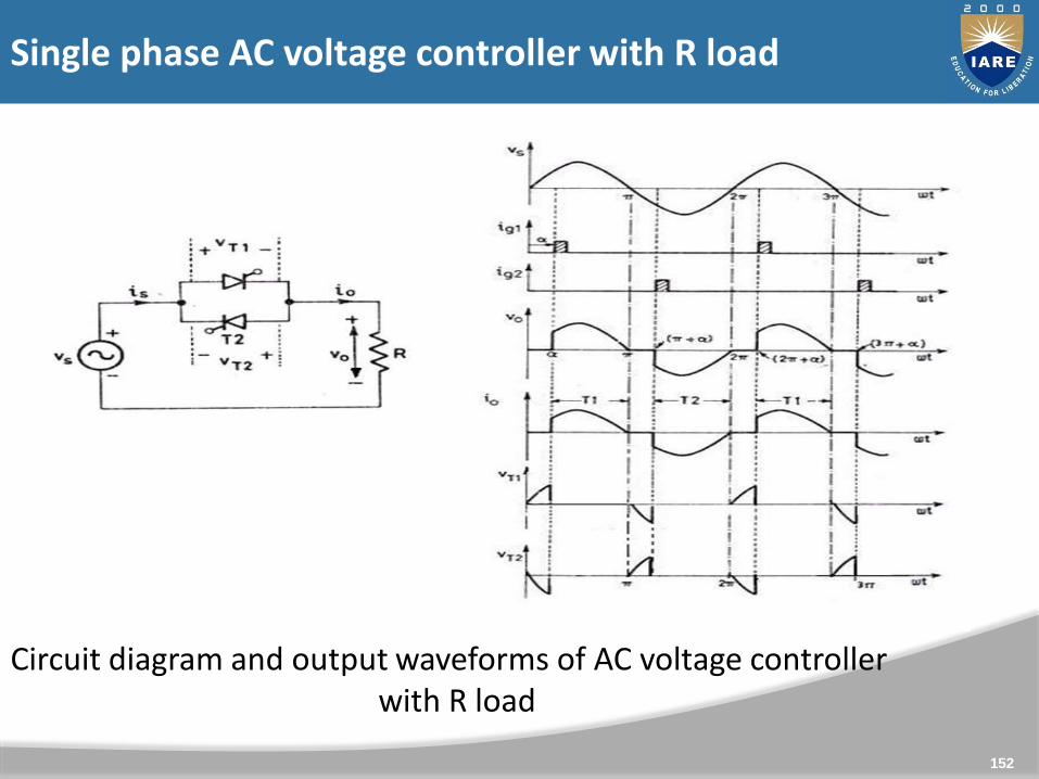
Circuit diagram and output waveforms of AC voltage controller with R load
Single phase AC voltage controller with R load
Cont..
AC to AC voltage converters operates on the AC mains essentially to
regulate the output voltage. Portions of the supply sinusoid appear at
the load while the semiconductor switches block the remaining
portions. Several topologies have emerged along with voltage
regulation methods, most of which are linked to the development of
the semiconductor devices.
153
Cont..
154
155
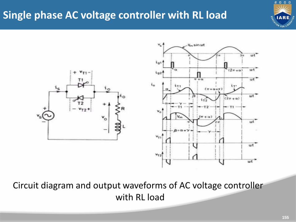
Circuit diagram and output waveforms of AC voltage controller with RL load
Single phase AC voltage controller with RL load
Cont..
With inductive loads the operation of the PAC is illustrated in
above figure. The current builds up from zero in each cycle. It
quenches not at the zero crossing of the applied voltage as with
the resistive load but after that instant. The supply voltage thus
continues to be impressed on the load till the load current
returns to zero. A single-pulse trigger for the TRIAC) or the anti
parallel SCR has no effect on the devices if it (or the anti-parallel
device) is already in conduction in the reverse direction.
156
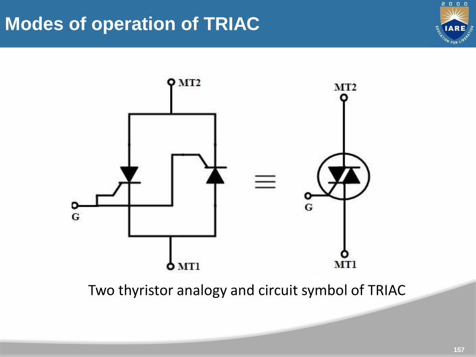
157
Two thyristor analogy and circuit symbol of TRIAC
Modes of operation of TRIAC
Cont..
The triac is an important member of the thyristor family of
devices. It is a bidirectional device that can pass the current in
both forward and reverse biased conditions and hence it is an
AC control device. The triac is equivalent to two back to back
SCRs connected with one gate terminal as shown in figure. The
triac is an abbreviation for a TRIode AC switch. TRI means that
the device consisting of three terminals and AC means that it
controls the AC power or it can conduct in both directions of
alternating current.
158
Cont..
159
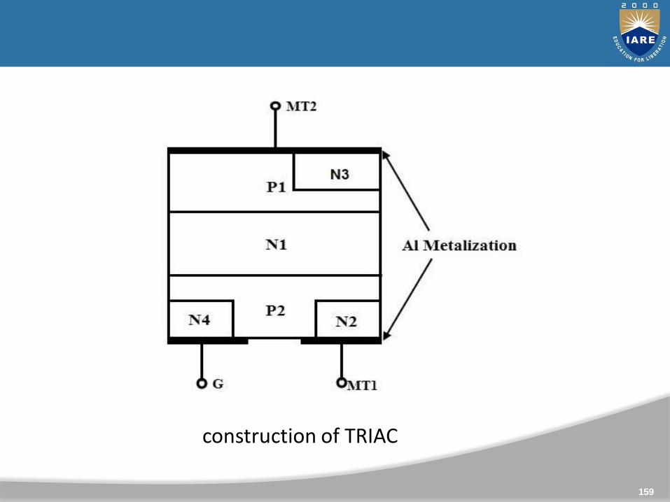
construction of TRIAC
Cont..
160
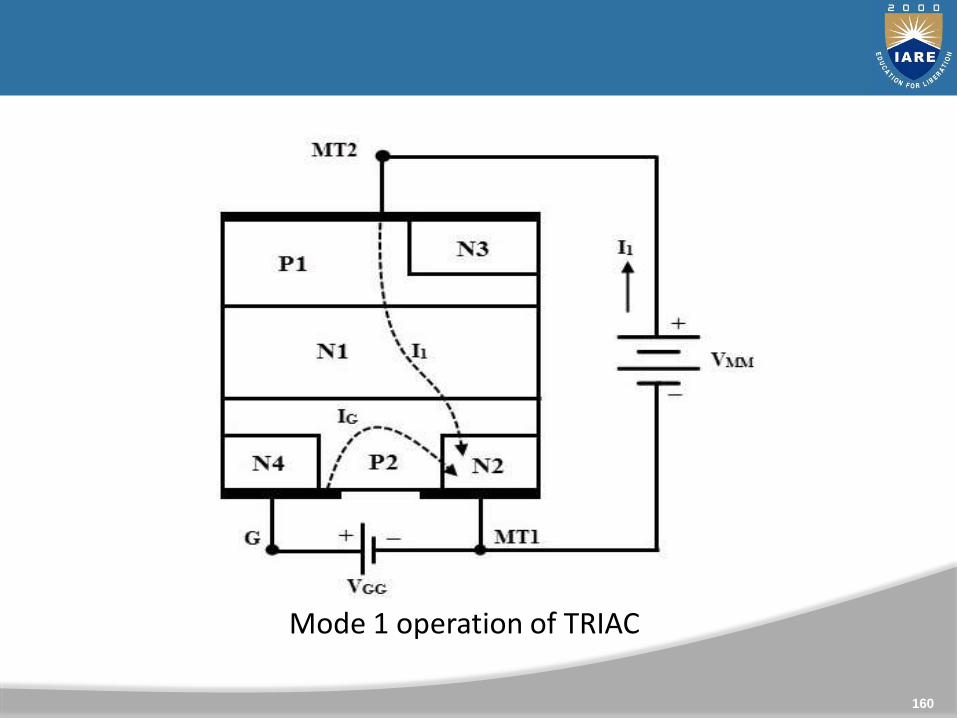
Mode 1 operation of TRIAC
Cont..
161
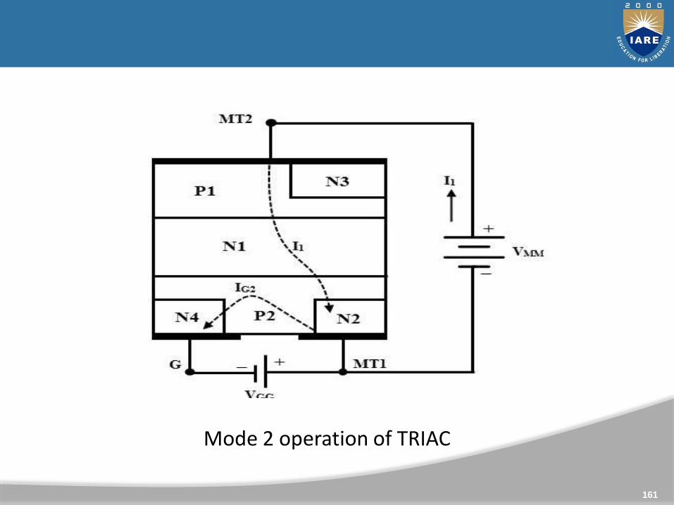
Mode 2 operation of TRIAC
Cont..
162
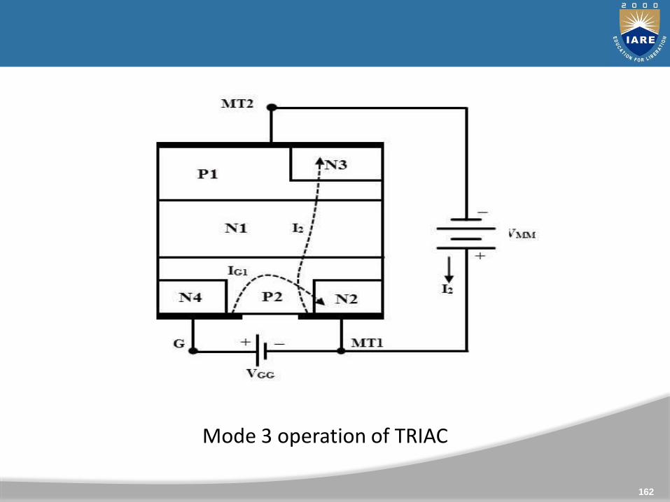
Mode 3 operation of TRIAC
Cont..
163
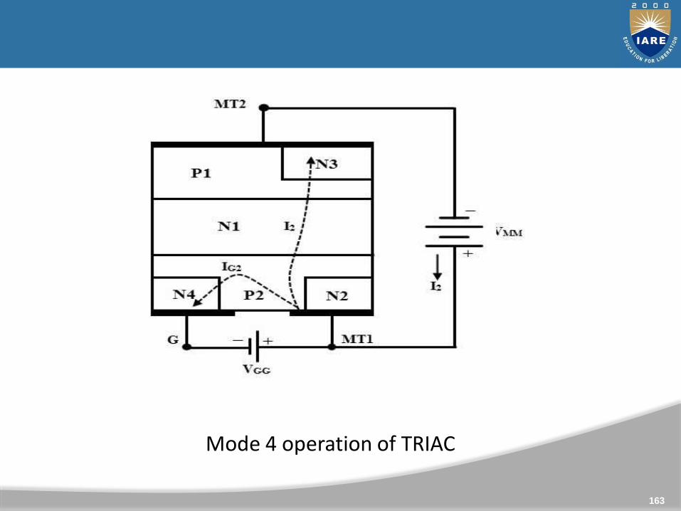
Mode 4 operation of TRIAC
Cont..
164
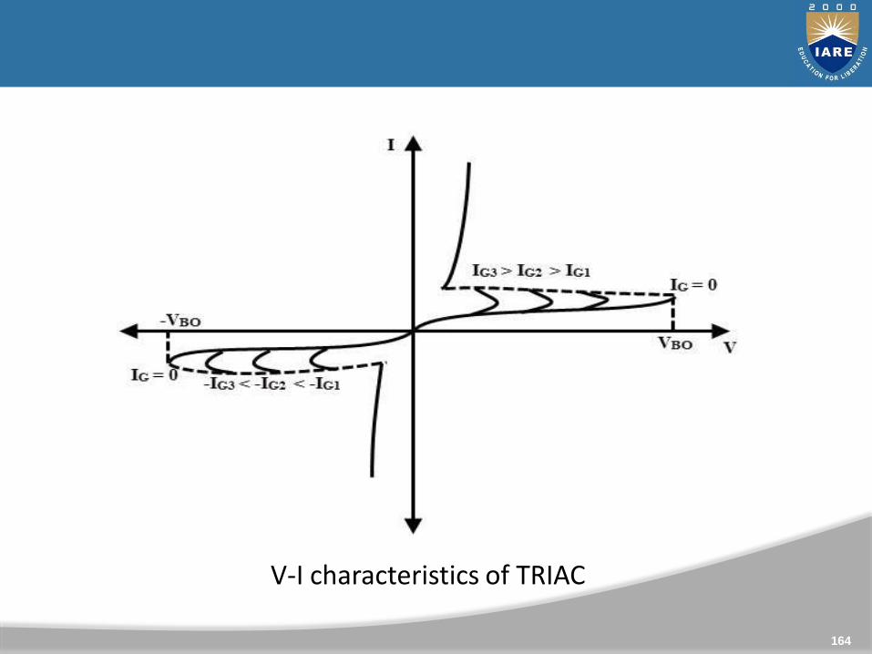
V-I characteristics of TRIAC
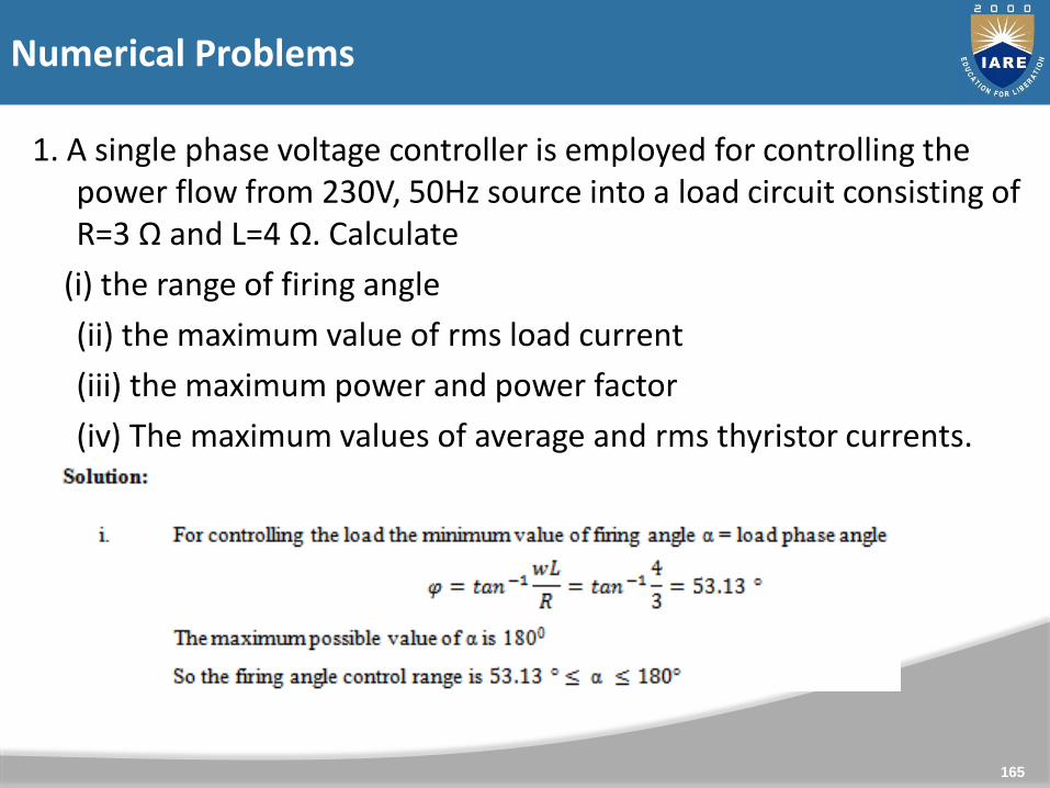
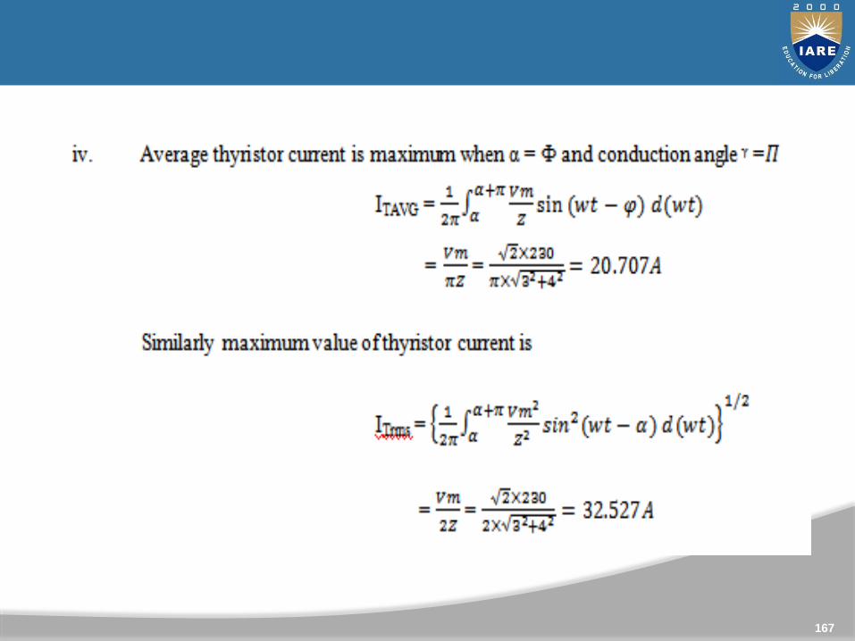
1. A single phase voltage controller is employed for controlling the power flow from 230V, 50Hz source into a load circuit consisting of R=3 Ω and L=4 Ω. Calculate
(i) the range of firing angle
(ii) the maximum value of rms load current
(iii) the maximum power and power factor
(iv) The maximum values of average and rms thyristor currents.
165
Numerical Problems
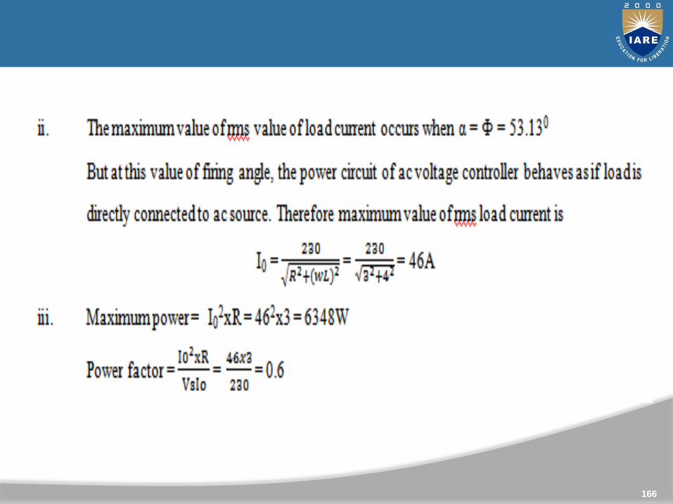
Cont..
166
Cont..
167
2. An ac voltage controller uses a TRIAC for phase angle control of a
resistive load of 100Ω. Calculate the value of delay angle for having
an rms load voltage of 220 volts. Also calculate the rms value of
TRIAC current. Assume the rms supply voltage to be 230V.
3. The ac voltage controller uses on-off control for heating a resistive
load of R = 4 ohms and the input voltage is Vs = 208V, 60Hz. If the
desired output power is PO = 3KW, determine the
duty cycle δ
input power factor
Sketch waveforms for the duty cycle obtained in (a)
168
The Cycloconverter has four thyristors divided into a positive and
negative bank of two thyristors each. When positive current flows in the
load, the output voltage is controlled by phase control of the two
positive bank thyristors whilst the negative bank thyristors are kept off
and vice versa when negative current flows in the load. An idealized
output waveform for a sinusoidal load current and a 45 degrees load
phase angle is shown in Figure
169
Cyclo converters
Cont..
170
Block diagram of cycloconverters
Cont..
171
circuit diagram of cycloconverter
Cont..
172
Input and output waveforms of cycloconverter
Basically, these are divided into two main types, and are given below
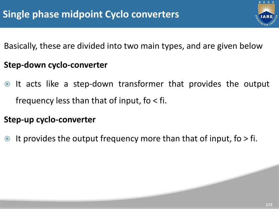
Step-down cyclo-converter
It acts like a step-down transformer that provides the output
frequency less than that of input, fo < fi.
Step-up cyclo-converter
It provides the output frequency more than that of input, fo > fi.
173
Single phase midpoint Cyclo converters
Cont..
174
circuit diagram of midpoint cycloconverter
Cont..
175
Input and output waveforms of midpoint cycloconverter
The equivalent circuit of a cyclo-converter is shown in figure
below. Here each two quadrant phase controlled converter is
represented by a voltage source of desired frequency and
consider that the output power is generated by the alternating
current and voltage at desired frequency.
The diodes connected in series with each voltage source
represent the unidirectional conduction of each two quadrant
converter. If the output voltage ripples of each converter are
neglected, then it becomes ideal and represents the desired
output voltage.
176
Bridge configuration of single phase Cyclo converter
Cont..
177
Block diagram of bridge type cycloconverter
Cont..
178
cycloconverter waveforms
Cont..
179
Circuit diagram of bridge type cycloconverter
Cont..
180
Input and output waveforms of bridge type cycloconverter
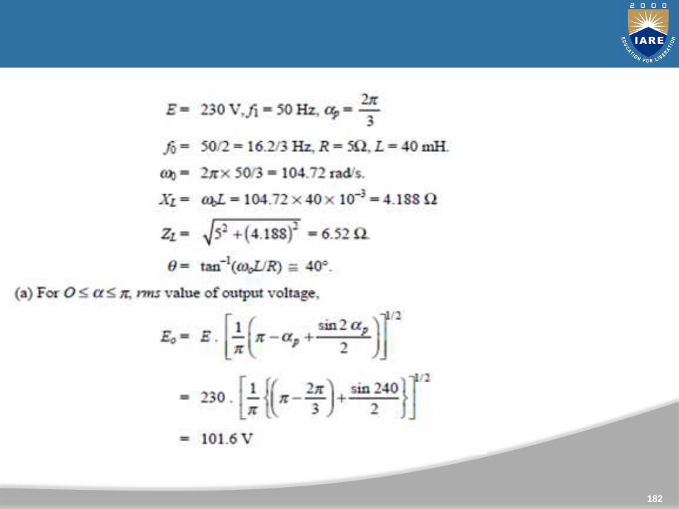
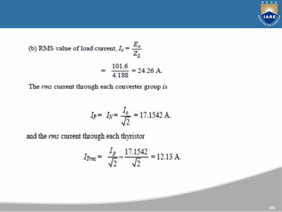
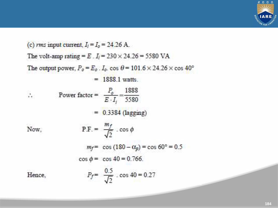
1. A single-phase to single-phase cycloconverter is supplying and
inductive load comprising of a Resistance of 5Ω and an inductance
of 40 mH from a 230 V, 50 Hz single-phase supply It is Required to
provide an output frequency which is 1/3 of the input frequency. If
the converters are Operated as semi converter such that and firing
delay angle is120°. Neglecting the Harmonic content of load
voltage, determine:
(a) rms value of output voltage.
(b) rms current of each thyristor and
(c) input power factor.181
Numerical Problems
Cont..
Solution:
182
Cont..
183
Cont..
184
2. In a standard A single-phase bridge-type cyclo-converter has input voltage
of 230V, 50Hz and load of R=10Ω. Output frequency is one-third of input
frequency. For a firing angle delay of 30o, Calculate (i) rms value of output
voltage (ii) rms current of each converter (iii) rms current of each thyristor
(iv) input power factor.
3. A single-phase to single-phase mid-point cyclo-converter is delivering power
to a resistive load. The supply transformer has turns ratio of 1: 1: 1. The
frequency ratio is fo/fs = 1/5. The firing angle delay α for all the four SCRs
are the same. Sketch the time variations of the following waveforms for α =
0° and α = 30°(a) Supply voltage (b) Output current and (c) Supply current.
Indicate the conduction of various thyristors also.185
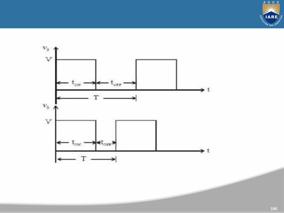
A chopper uses high speed to connect and disconnect from a
source load. A fixed DC voltage is applied intermittently to the
source load by continuously triggering the power switch ON/OFF.
The period of time for which the power switch stays ON or OFF is
referred to as the chopper’s ON and OFF state times, respectively.
Choppers are mostly applied in electric cars, conversion of wind
and solar energy, and DC motor regulators.
187
Introduction to Choppers
Cont..
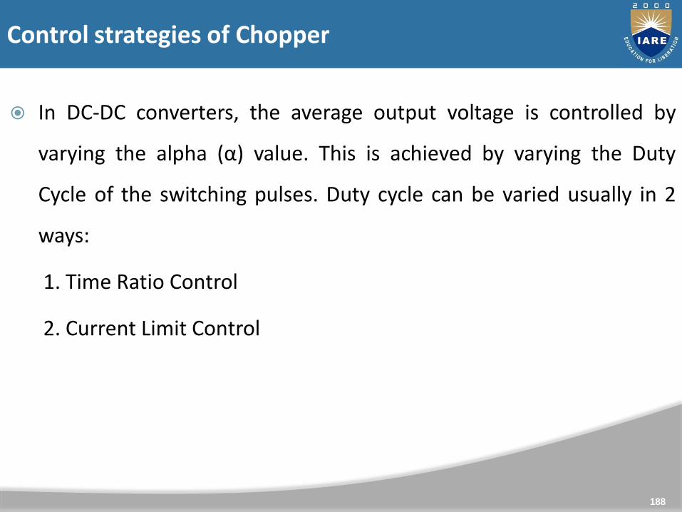
In DC-DC converters, the average output voltage is controlled by
varying the alpha (α) value. This is achieved by varying the Duty
Cycle of the switching pulses. Duty cycle can be varied usually in 2
ways:
1. Time Ratio Control
2. Current Limit Control
188
Control strategies of Chopper
Cont..
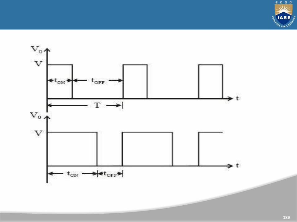
Pulse Width Modulation (PWM)
189
Cont..
Frequency Modulation Control (FMC)
190
Cont..
Current Limit Control
191
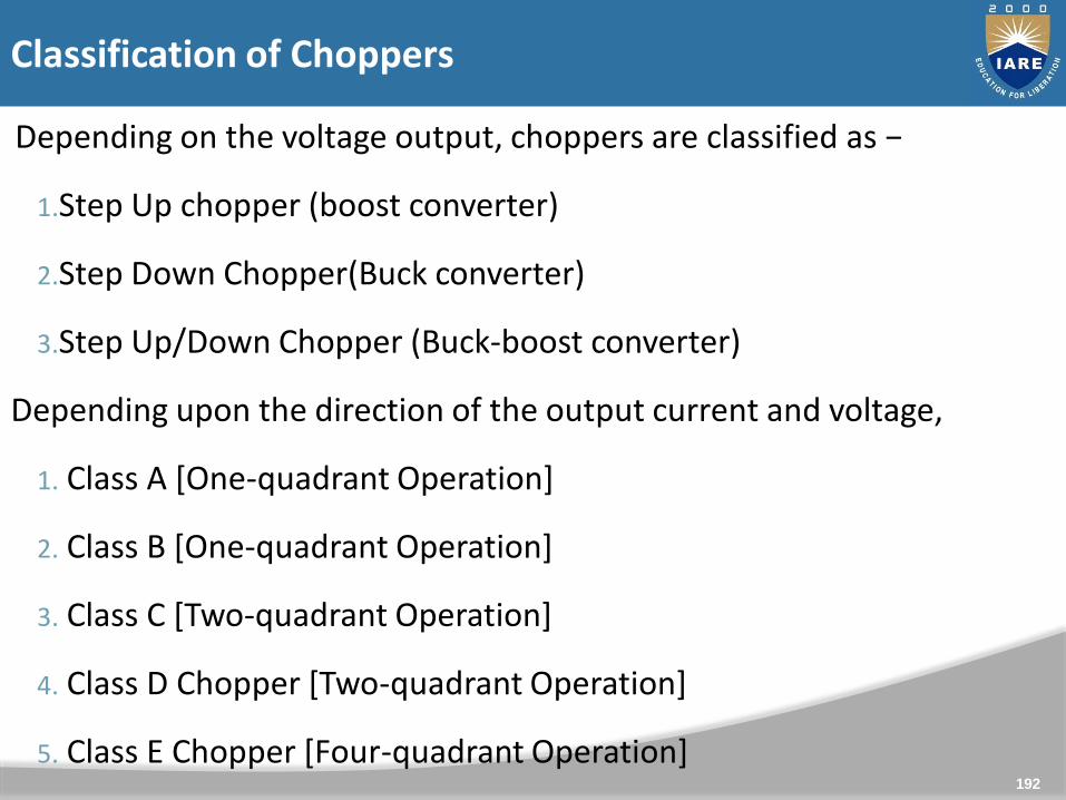
Depending on the voltage output, choppers are classified as −
1.Step Up chopper (boost converter)
2.Step Down Chopper(Buck converter)
3.Step Up/Down Chopper (Buck-boost converter)
Depending upon the direction of the output current and voltage,
1. Class A [One-quadrant Operation]
2. Class B [One-quadrant Operation]
3. Class C [Two-quadrant Operation]
4. Class D Chopper [Two-quadrant Operation]
5. Class E Chopper [Four-quadrant Operation]192
Classification of Choppers
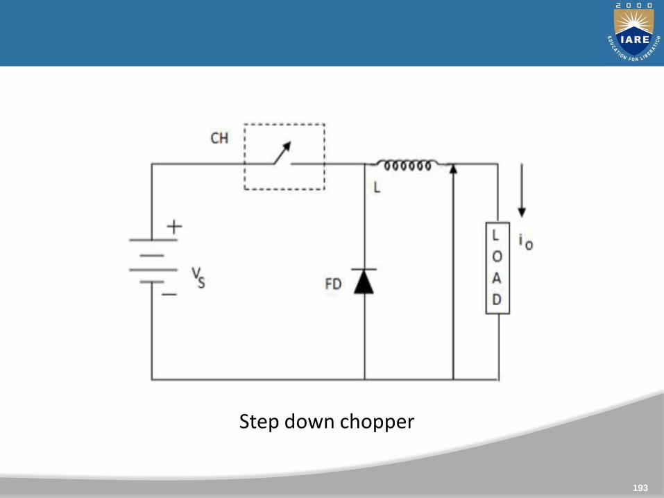
Cont..
193
Step down chopper
Cont..
194
Cont..
195
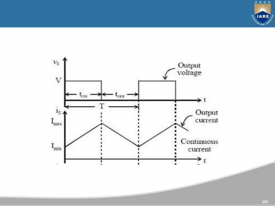
Input and output waveforms
196
Step Up Chopper
Cont..
197
Input and output waveforms of step up chopper
Cont..
198
Cont..
199
200
Step Up/ Step Down Chopper
Cont..
201
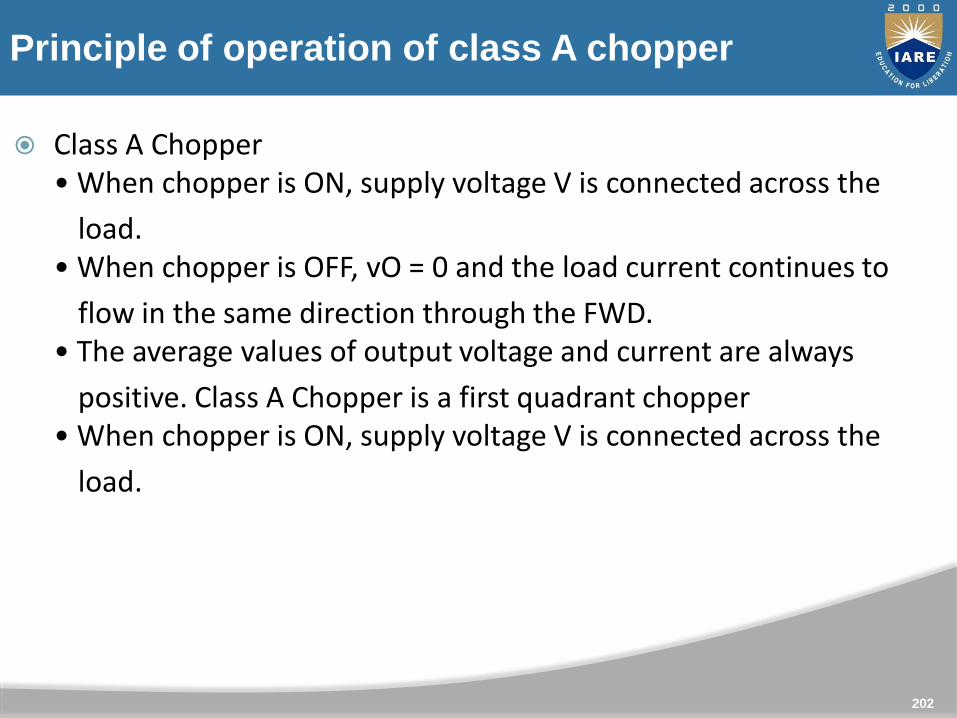
Class A Chopper • When chopper is ON, supply voltage V is connected across the
load.• When chopper is OFF, vO = 0 and the load current continues to
flow in the same direction through the FWD.• The average values of output voltage and current are always
positive. Class A Chopper is a first quadrant chopper• When chopper is ON, supply voltage V is connected across the
load.
202
Principle of operation of class A chopper
Cont..
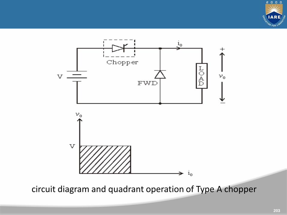
203
circuit diagram and quadrant operation of Type A chopper
Cont..
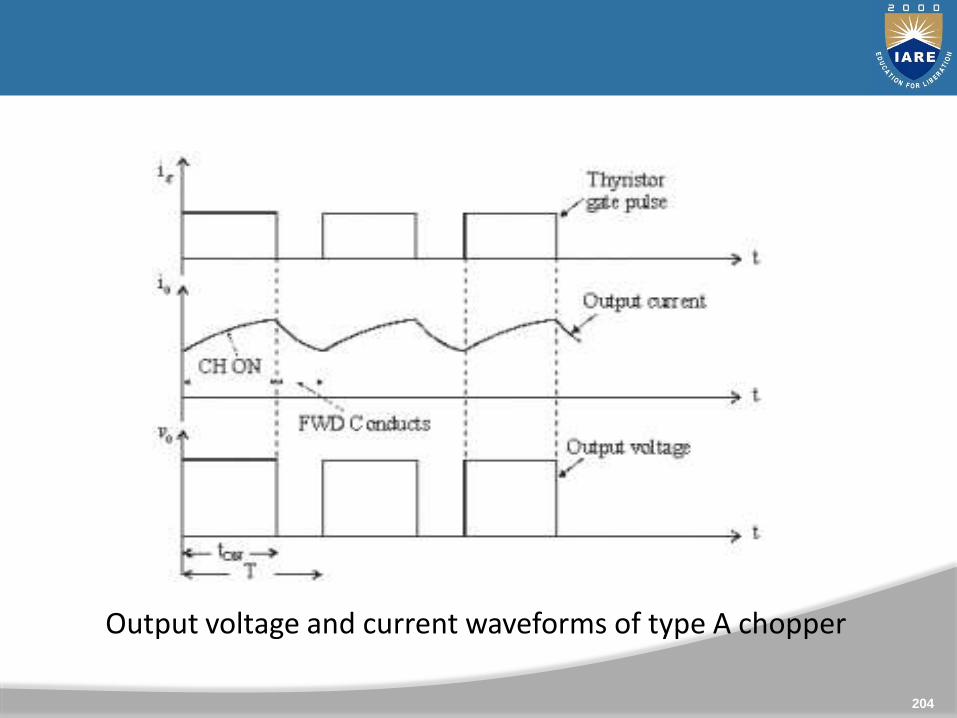
204
Output voltage and current waveforms of type A chopper
• When chopper is ON, E drives a current through L and R in a
direction opposite to that shown in figure.
• During the ON period of the chopper, the inductance L stores
energy.
• When Chopper is OFF, diode D conducts, and part of the energy stored in
inductor L is returned to the supply.
• Average output voltage is positive. Average output current is negative.
• Therefore Class B Chopper operates in second quadrant.
• In this chopper, power flows from load to source.
• Class B Chopper is used for regenerative braking of dc motor.
205
Class B Chopper
Cont..
206
circuit diagram and quadrant operation of Type B chopper
Cont..
207
Output voltage and current waveforms of type B chopper
208
Class C chopper
Cont..
209
Output voltage and current waveforms of type C chopper
Class D is a two quadrant chopper.• When both CH1 and CH2 are triggered simultaneously, the output
voltage vO = V and output current flows through the load.• When CH1 and CH2 are turned OFF, the load current continues to
flow in the same direction through load, D1 and D2 , due to the
energy stored in the inductor L.• Output voltage vO = – V.• Average load voltage is positive if chopper ON time is more than
the OFF time• Average output voltage becomes negative if tON < tOFF .• Hence the direction of load current is always positive but load
voltage can be positive or negative.
210
Class D chopper
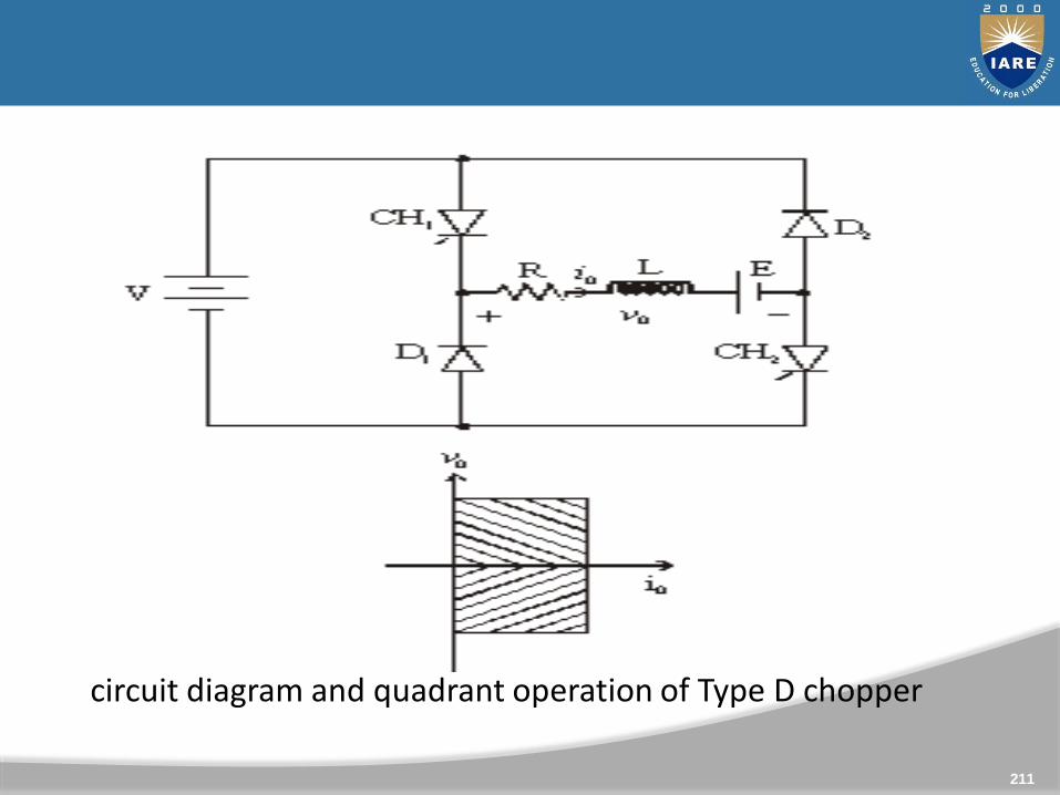
Cont..
211
circuit diagram and quadrant operation of Type D chopper
Cont..
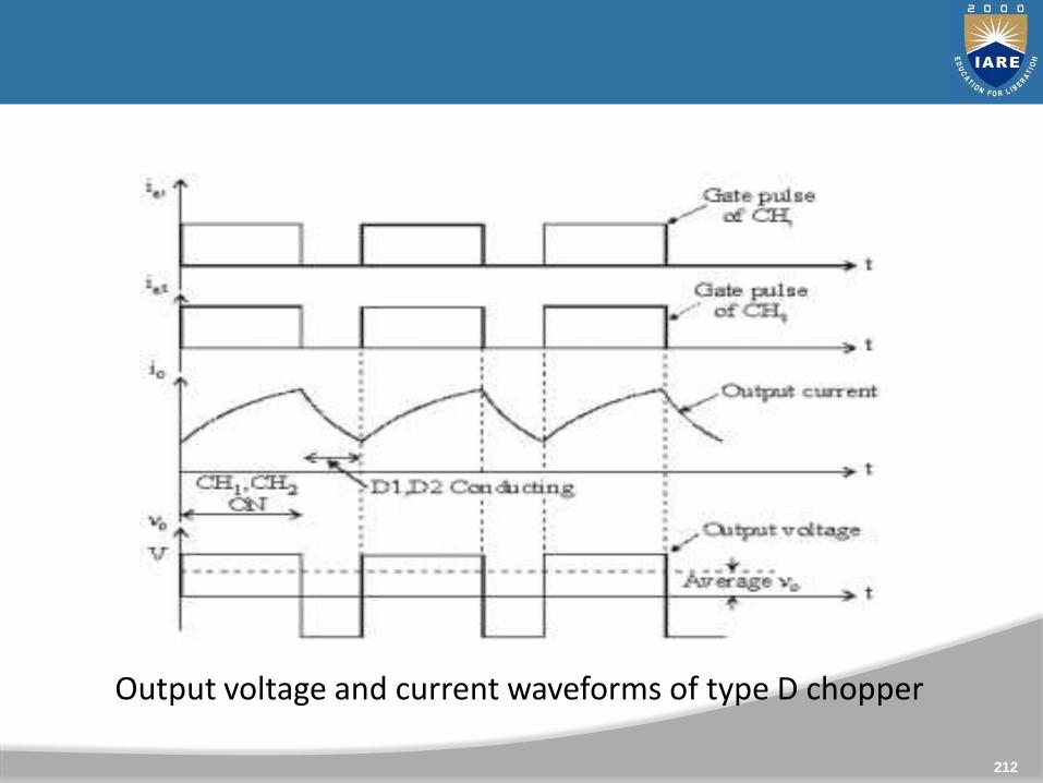
212
Output voltage and current waveforms of type D chopper
Class E is a four quadrant chopper• When CH1 and CH4 are triggered, output current iO flows in
positive direction through CH1 and CH4, and with output voltage
vO = V.• This gives the first quadrant operation.• When both CH1 and CH4 are OFF, the energy stored in the inductor
L drives iO through D2 and D3 in the same direction, but output
voltage vO = -V.• Therefore the chopper operates in the fourth quadrant.
213
Class E Chopper
Cont..
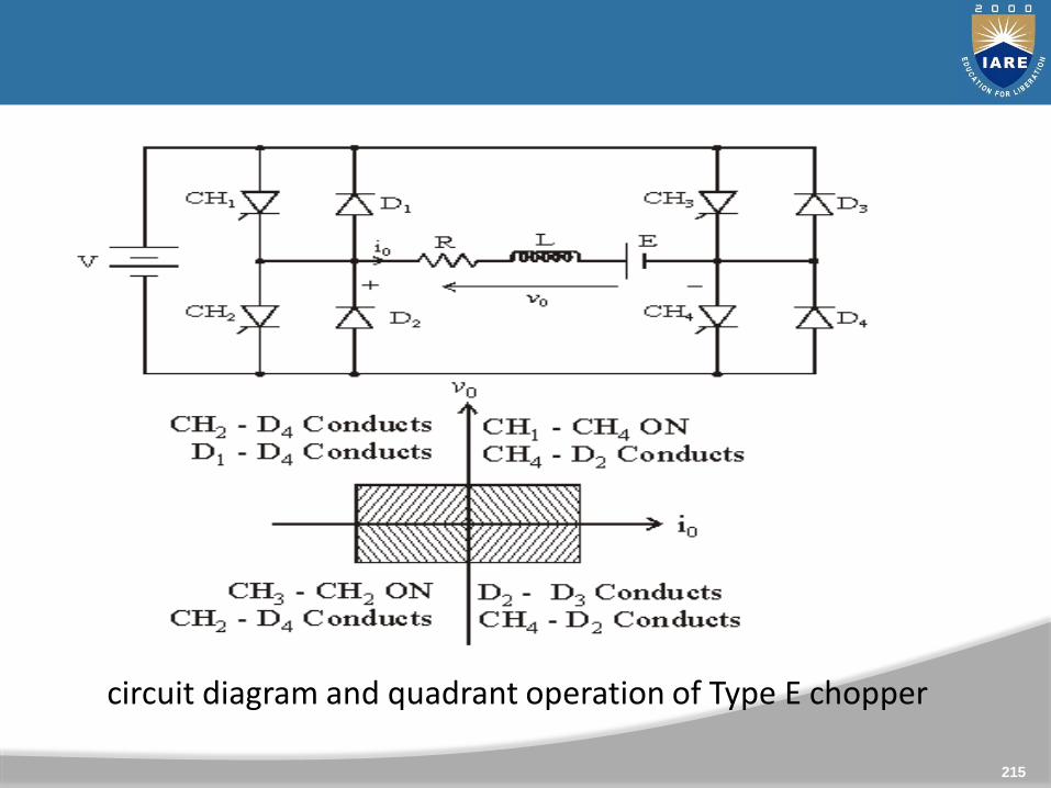
• When CH2 and CH3 are triggered, the load current iO flows in
opposite direction & output voltage vO = -V.• Since both iO and vO are negative, the chopper operates in
third quadrant.• When both CH2 and CH3 are OFF, the load current iO continues
to flow in the same direction D1 and D4 and the output voltage
vO = V.• Therefore the chopper operates in second quadrant as vO is
positive but iO is negative.
214
Cont..
215
circuit diagram and quadrant operation of Type E chopper
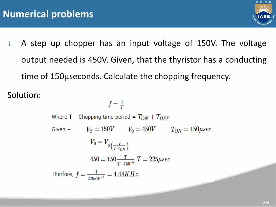
1. A step up chopper has an input voltage of 150V. The voltage
output needed is 450V. Given, that the thyristor has a conducting
time of 150μseconds. Calculate the chopping frequency.
Solution:
216
Numerical problems
Cont..
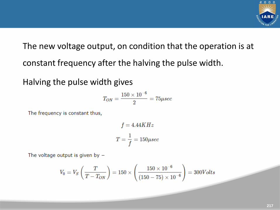
The new voltage output, on condition that the operation is at
constant frequency after the halving the pulse width.
Halving the pulse width gives
217
2. In a type A chopper, the input supply voltage is 230 V the load
resistance is 10Ω and there is a voltage drop of 2 V across the
chopper thyristor when it is on. For a duty ratio of 0.4, calculate the
average and rms values of the output voltage. Also find the chopper
efficiency
3. A step-up chopper supplies a load of 480 V from 230 V dc supply.
Assuming the non conduction period of the thyristor to be 50
microsecond, find the on time of the thyristor
218
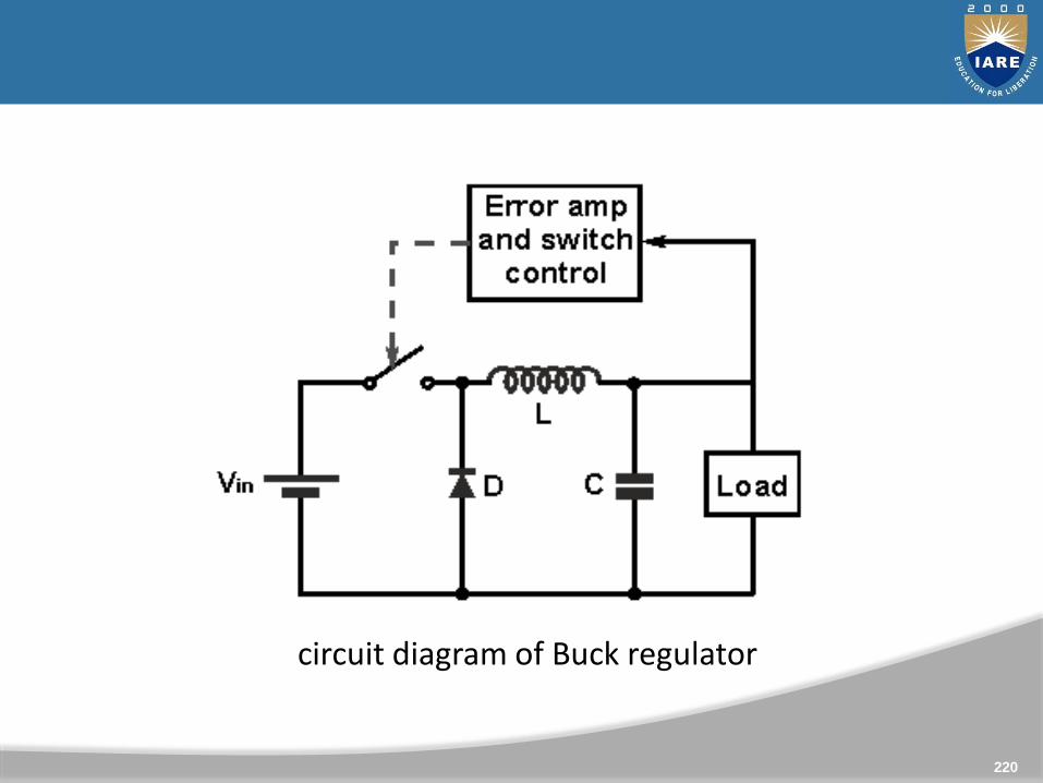
With power being a key parameter in many designs, step down or "buck"
regulators are widely used.
Although a resistor would enable voltage to be dropped, power is lost, and
in applications such as the many battery powered items used today, power
consumption is a crucial element.
As a result step down switch mode converters or as they are more
commonly termed, buck regulators are widely used.
Linear step down
The most basic form of step down transition is to use a resistor as a
potential divider or voltage dropper. In some cases a zener diode may also
be used to stabilize the voltage.
219
Buck regulator
Cont..
220
circuit diagram of Buck regulator
Cont..
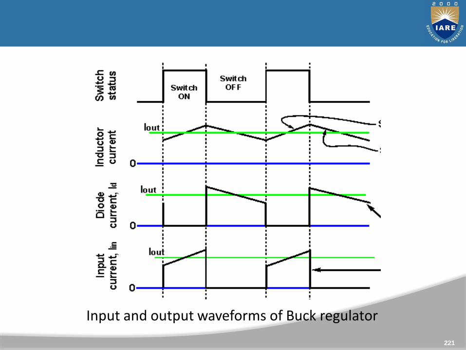
221
Input and output waveforms of Buck regulator
222
circuit diagram of Boost regulator
Boost regulator
Cont..
223
Input and output waveforms of Boost regulator
The buck-boost DC-DC converter offers a greater level of capability than
the buck converter of boost converter individually, it as expected it extra
components may be required to provide the level of functionality needed.
There are several formats that can be used for buck-boost converters:
+Vin, -Vout: This configuration of a buck-boost converter circuit uses the
same number of components as the simple buck or boost converters.
However this buck-boost regulator or DC-DC converter produces a negative
output for a positive input. While this may be required or can be
accommodated for a limited number of applications, it is not normally the
most convenient format.
224
Buck boost regulator
Cont..
225
circuit diagram of buck boost regulator
Cont..
When the switch in closed, current builds up through the inductor.
When the switch is opened the inductor supplies current through the
diode to the load.
Obviously the polarities (including the diode) within the buck-boost
converter can be reversed to provide a positive output voltage from a
negative input voltage.
+Vin, +Vout: The second buck-boost converter circuit allows both input
and output to be the same polarity. However to achieve this, more
components are required. The circuit for this buck boost converter is
shown below.
226
Cont..
227
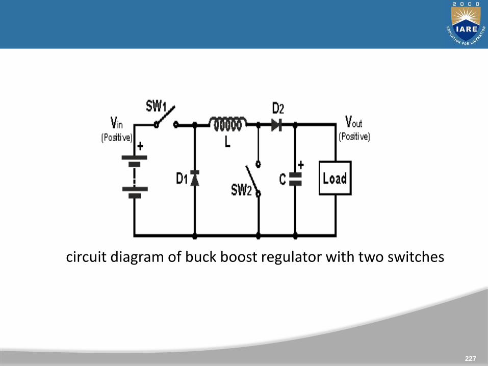
circuit diagram of buck boost regulator with two switches
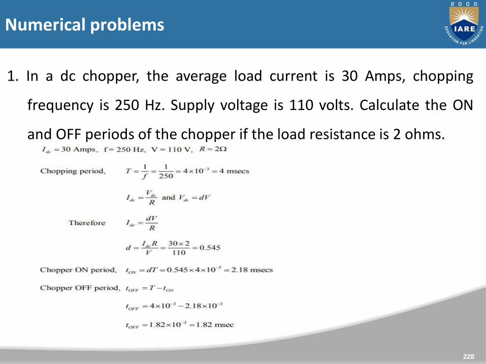
1. In a dc chopper, the average load current is 30 Amps, chopping
frequency is 250 Hz. Supply voltage is 110 volts. Calculate the ON
and OFF periods of the chopper if the load resistance is 2 ohms.
228
Numerical problems
Cont..
2. A step up chopper has input voltage of 220 V and output voltage
of 660 V. If the non-conducting time of thyristor chopper is 100
micro sec compute the pulse width of output voltage. In case
the pulse width is halved for constant frequency operation , find
the new output voltage
3. A chopper operating from 220V dc supply with for a duty cycle of
0.5 and chopping frequency of 1KHz drives an R L load with R =
1Ω , L=1mH and E = 105V. Find whether the current is
continuous and also find the values of Imax and Imin.
229
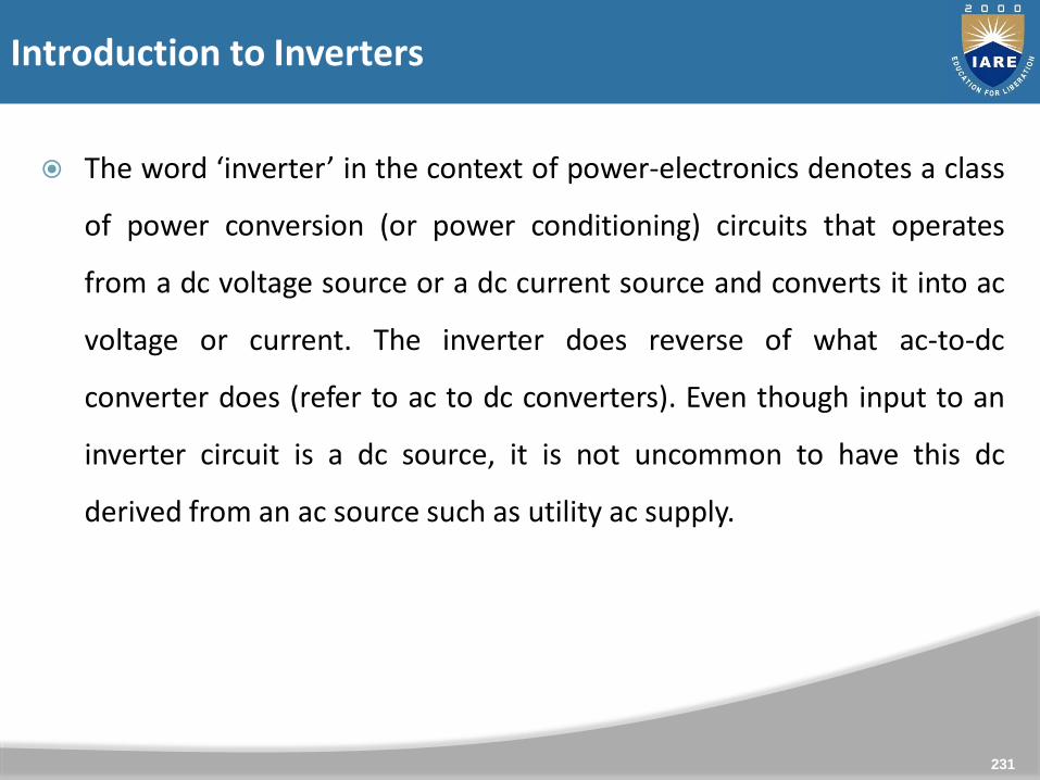
The word ‘inverter’ in the context of power-electronics denotes a class
of power conversion (or power conditioning) circuits that operates
from a dc voltage source or a dc current source and converts it into ac
voltage or current. The inverter does reverse of what ac-to-dc
converter does (refer to ac to dc converters). Even though input to an
inverter circuit is a dc source, it is not uncommon to have this dc
derived from an ac source such as utility ac supply.
231
Introduction to Inverters
Cont..
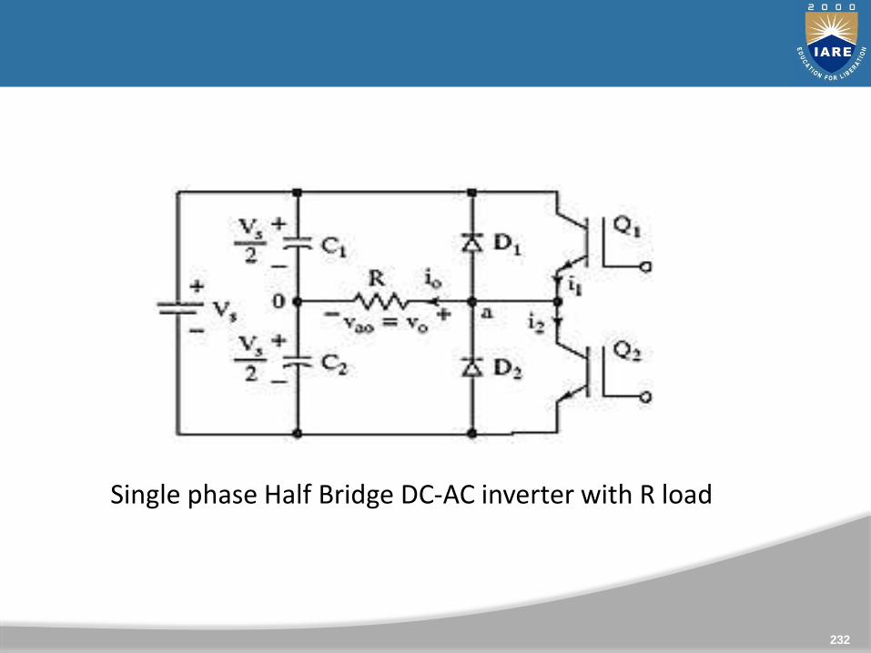
232
Single phase Half Bridge DC-AC inverter with R load
Cont..
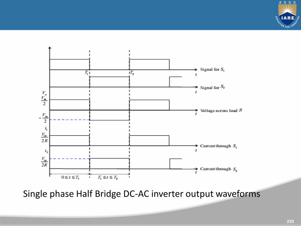
233
Single phase Half Bridge DC-AC inverter output waveforms
234
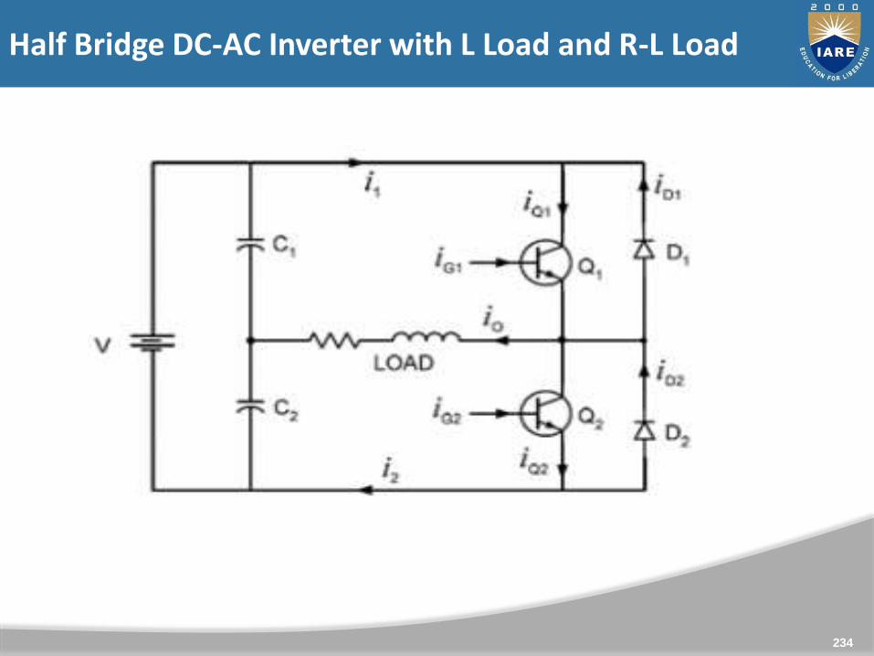
Half Bridge DC-AC Inverter with L Load and R-L Load
A single phase bridge DC-AC inverter is shown in Figure below.
The analysis of the single phase DC-AC inverters is done taking
into account following assumptions and conventions.
1) The current entering node a in Figure 8 is considered to be
positive.
2) The switches S1, S2, S3 and S4 are unidirectional, i.e. they
conduct current in one direction.
235
Operation of single phase full bridge inverter
Cont..
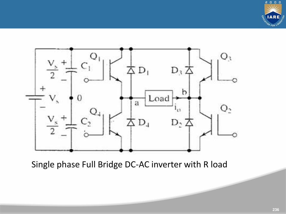
236
Single phase Full Bridge DC-AC inverter with R load
Cont..
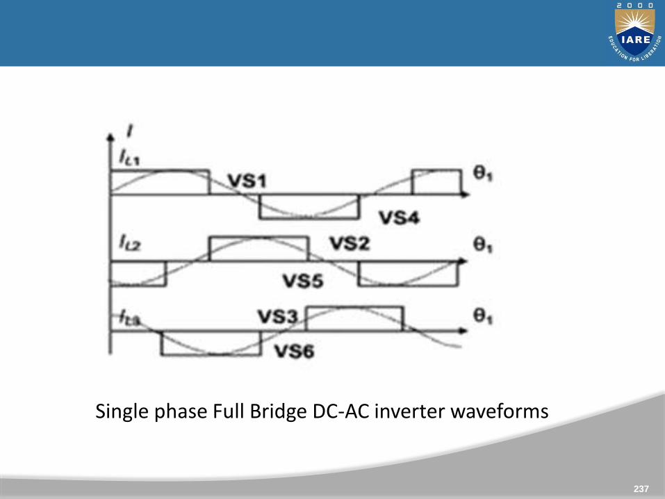
237
Single phase Full Bridge DC-AC inverter waveforms
238
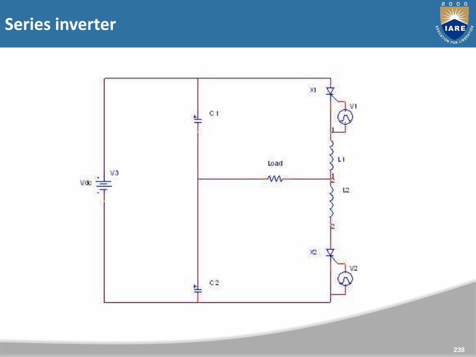
Series inverter
The single phase parallel inverter circuit consists of two SCRs T1 and
T2, an inductor L, an output transformer and a commutating
capacitor C. The output voltage and current are Vo and Io
respectively. The function of L is to make the source current
constant. During the working of this inverter, capacitor C comes
in parallel with the load via the transformer. So it is called a parallel
inverter.
239
Operation of parallel inverter
Cont..
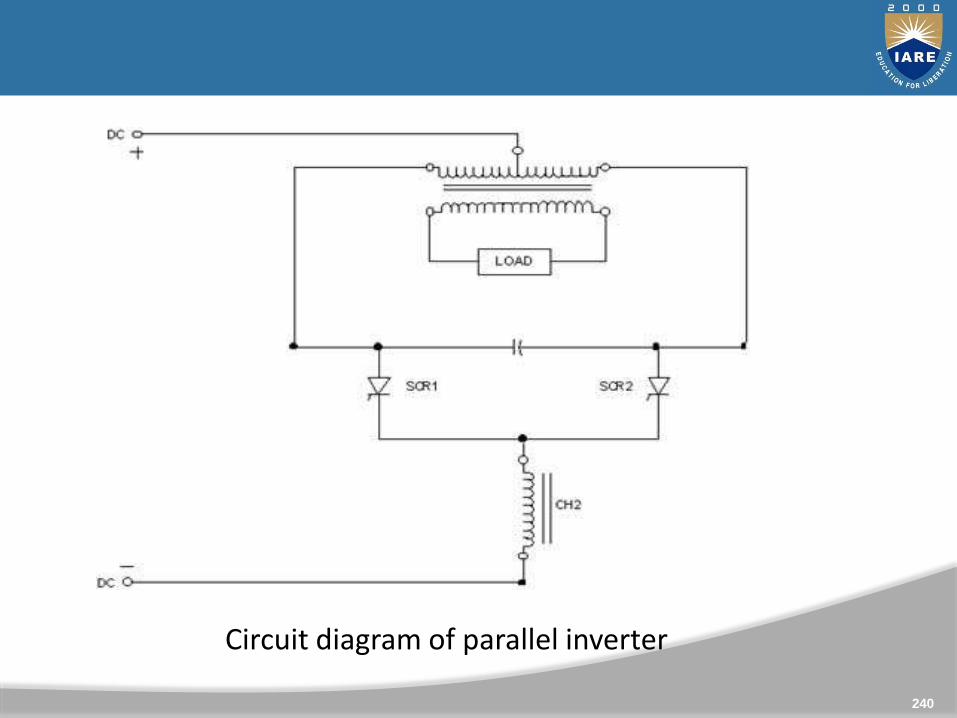
240
Circuit diagram of parallel inverter
Cont..
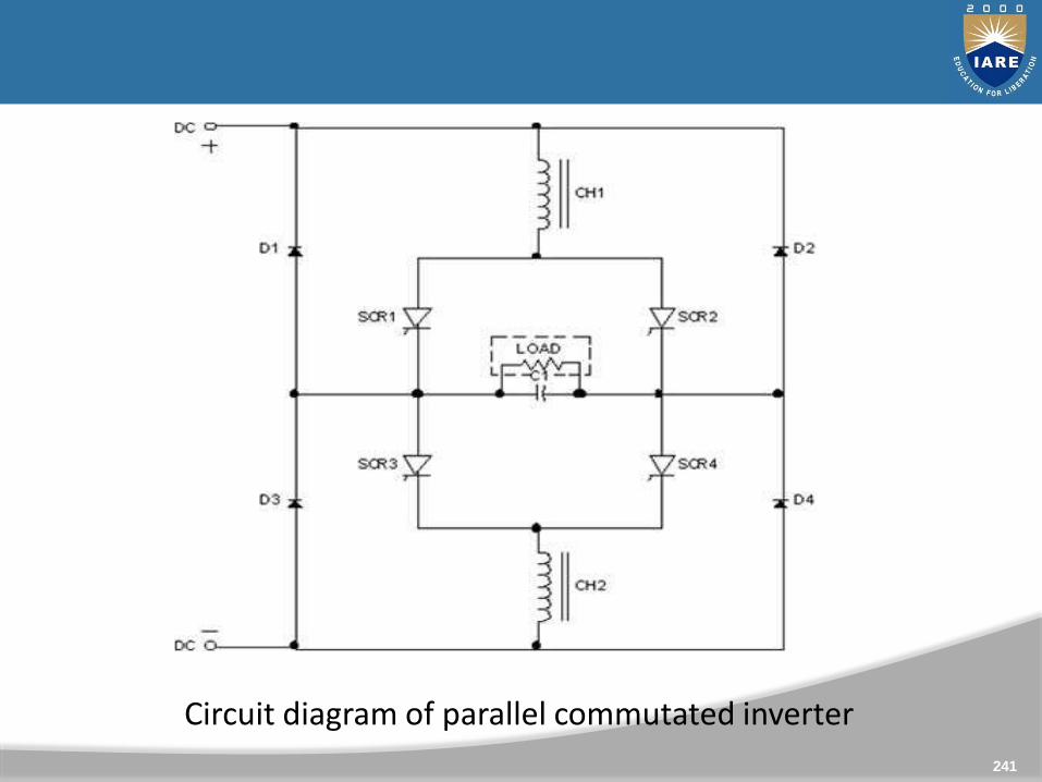
241
Circuit diagram of parallel commutated inverter
Three phase inverters are normally used for high power
applications. The advantages of a three phase inverter are:
The frequency of the output voltage waveform depends on the
switching rate of the swtiches and hence can be varied over a
wide range.
The direction of rotation of the motor can be reversed by
changing the output phase sequence of the inverter.
The ac output voltage can be controlled by varying the dc link
voltage.
242
Three Phase DC-AC Converters
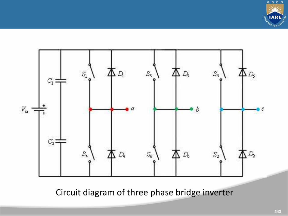
Cont..
243
Circuit diagram of three phase bridge inverter
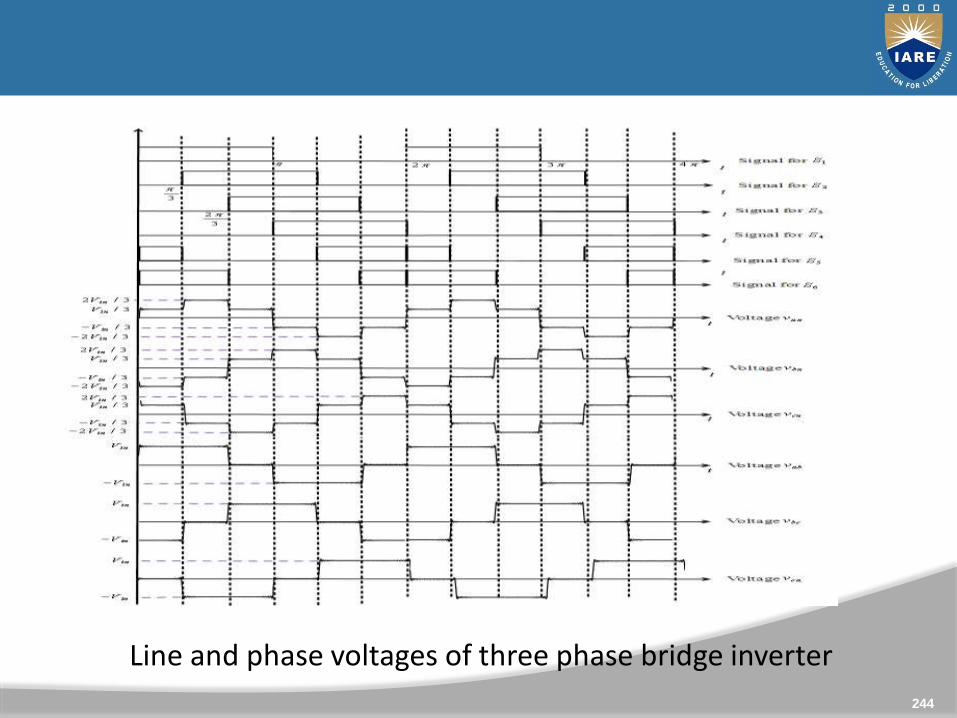
Cont..
244
Line and phase voltages of three phase bridge inverter
Cont..
245
In this mode of conduction, each electronic device is in a conductionstate for 120°. It is most suitable for a delta connection in a loadbecause it results in a six-step type of waveform across any of itsphases. Therefore, at any instant only two devices are conductingbecause each device conducts at only 120°.
The terminal A on the load is connected to the positive end while theterminal B is connected to the negative end of the source. Theterminal C on the load is in a condition called floating state.Furthermore, the phase voltages are equal to the load voltages asshown below.
Phase voltages = Line voltages
VAB = V
VBC = −V/2
VCA = −V/2246
Three Phase DC-AC Converters with 120 degree conduction mode
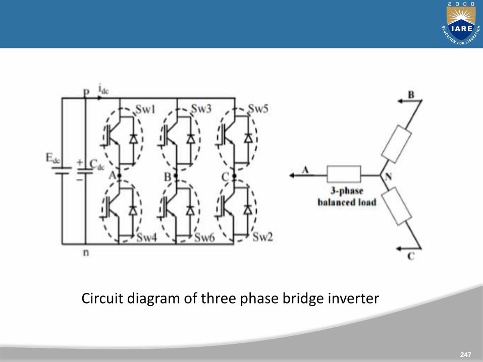
Cont..
247
Circuit diagram of three phase bridge inverter
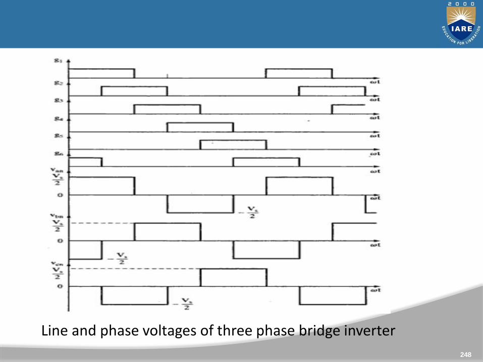
Cont..
248
Line and phase voltages of three phase bridge inverter
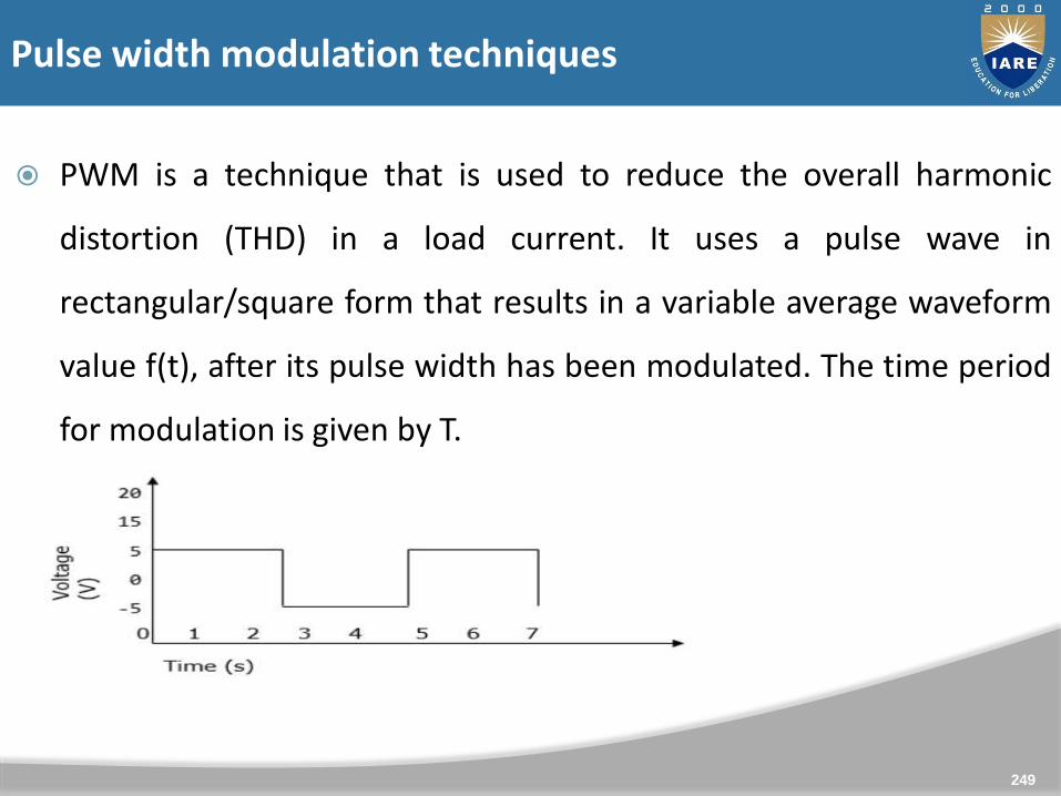
PWM is a technique that is used to reduce the overall harmonic
distortion (THD) in a load current. It uses a pulse wave in
rectangular/square form that results in a variable average waveform
value f(t), after its pulse width has been modulated. The time period
for modulation is given by T.
249
Pulse width modulation techniques
250
Sinusoidal Pulse Width Modulation
251
Multiple PWM
Cont..
252
Waveform of multiple PWM technique
253
schematic diagram of Half bridge PWM inverter
Operation of sinusoidal pulse width modulation
Cont..
254
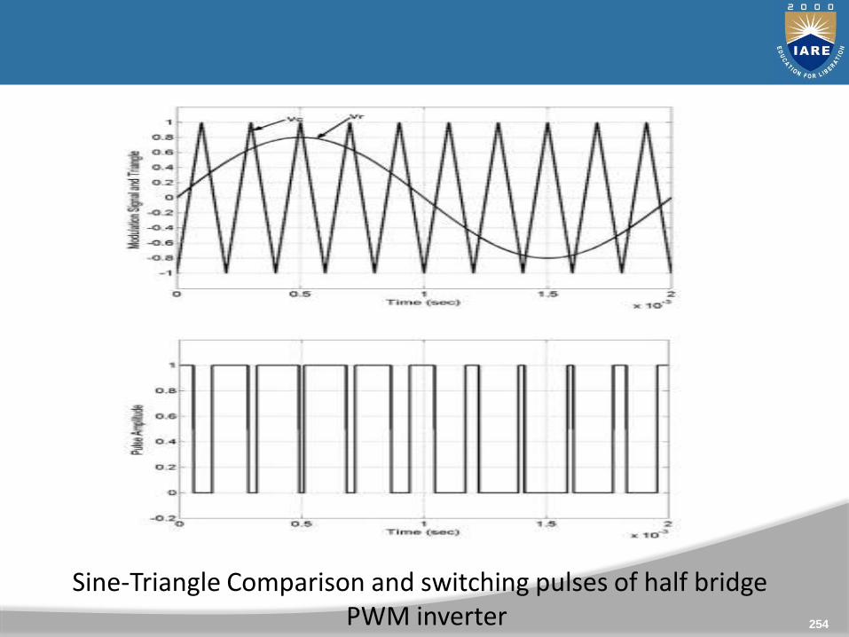
Sine-Triangle Comparison and switching pulses of half bridge PWM inverter
255
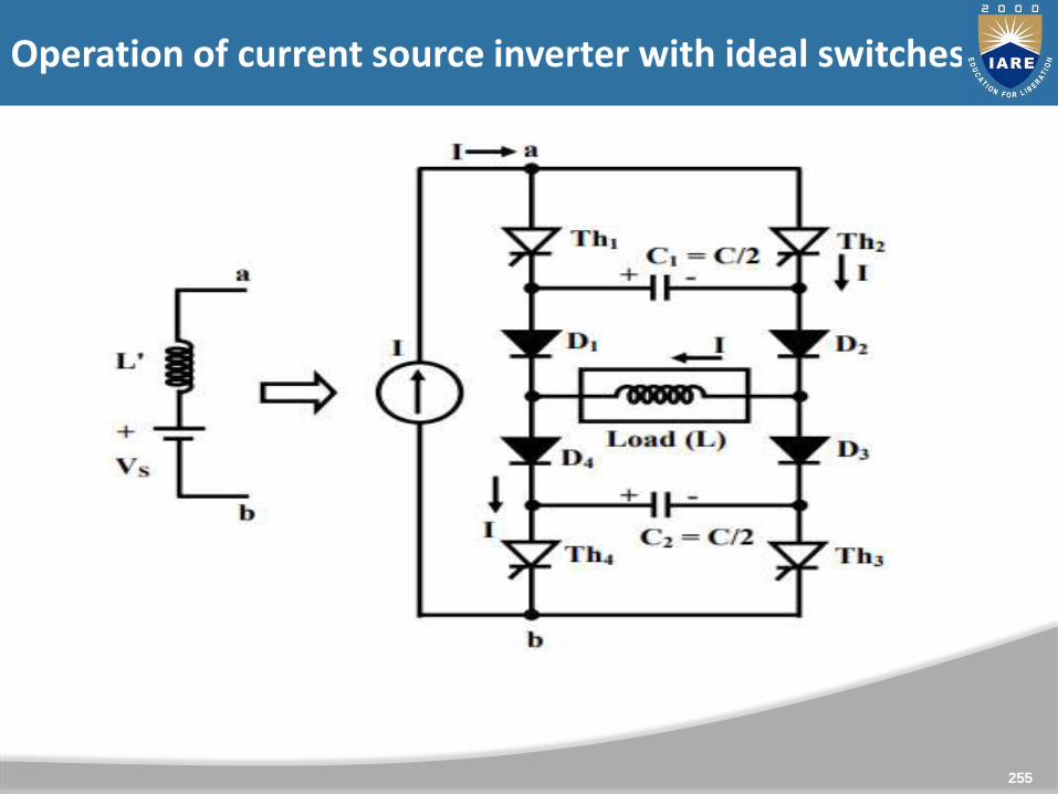
Operation of current source inverter with ideal switches
Cont..
256
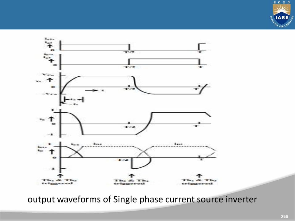
output waveforms of Single phase current source inverter
Cont..
257
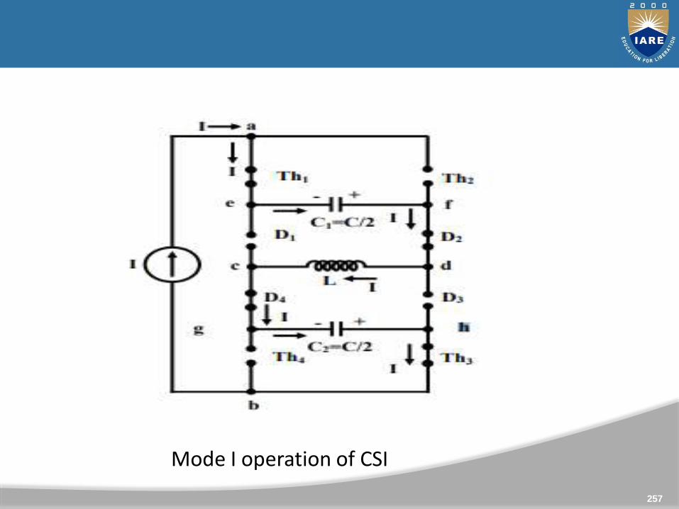
Mode I operation of CSI
Cont..
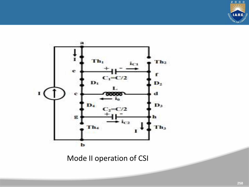
258
Mode II operation of CSI
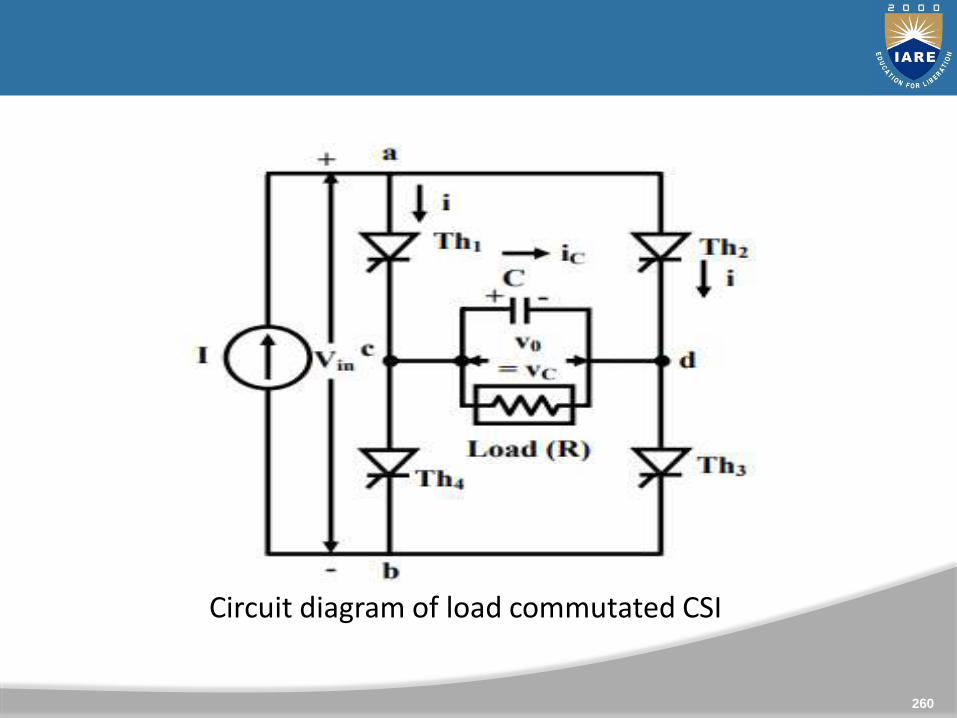
The power switching devices used here is the same, i.e. fourThyristors only in a full- bridge configuration. The positivedirection for load current and voltage is shown in Fig. 5.40Before t = 0, the capacitor voltage is , i.e. the capacitor has leftplate negative and right plate positive. At that time, the thyristorpair, Th2 & Th4 was conducting. When (at t = 0), the thyristorpair, Th1 & Th3 is triggered by the pulses fed at the gates, theconducting thyristor pair, Th2 & Th4 is reverse biased by thecapacitor voltage C = −Vv 1 , and turns off immediately. Thecurrent path is through Th1, load (parallel combination of R & C),Th3, and the source. The current in the thyristors is ITi , theoutput current is
Iac= I
259
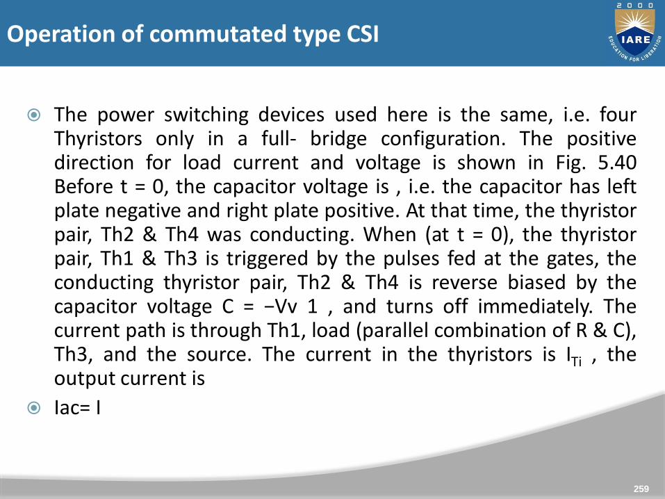
Operation of commutated type CSI
Cont..
260
Circuit diagram of load commutated CSI
Cont..
261
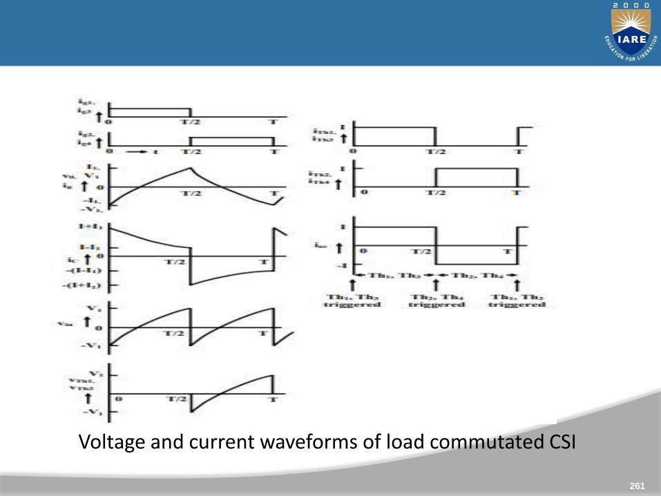
Voltage and current waveforms of load commutated CSI
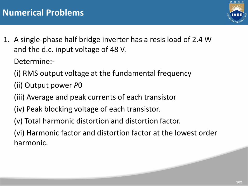
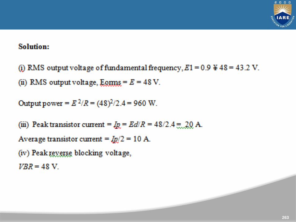
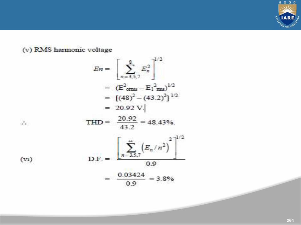
1. A single-phase half bridge inverter has a resis load of 2.4 W and the d.c. input voltage of 48 V.
Determine:-
(i) RMS output voltage at the fundamental frequency
(ii) Output power P0
(iii) Average and peak currents of each transistor
(iv) Peak blocking voltage of each transistor.
(v) Total harmonic distortion and distortion factor.
(vi) Harmonic factor and distortion factor at the lowest order harmonic.
262
Numerical Problems
Cont..
263
Cont..
264
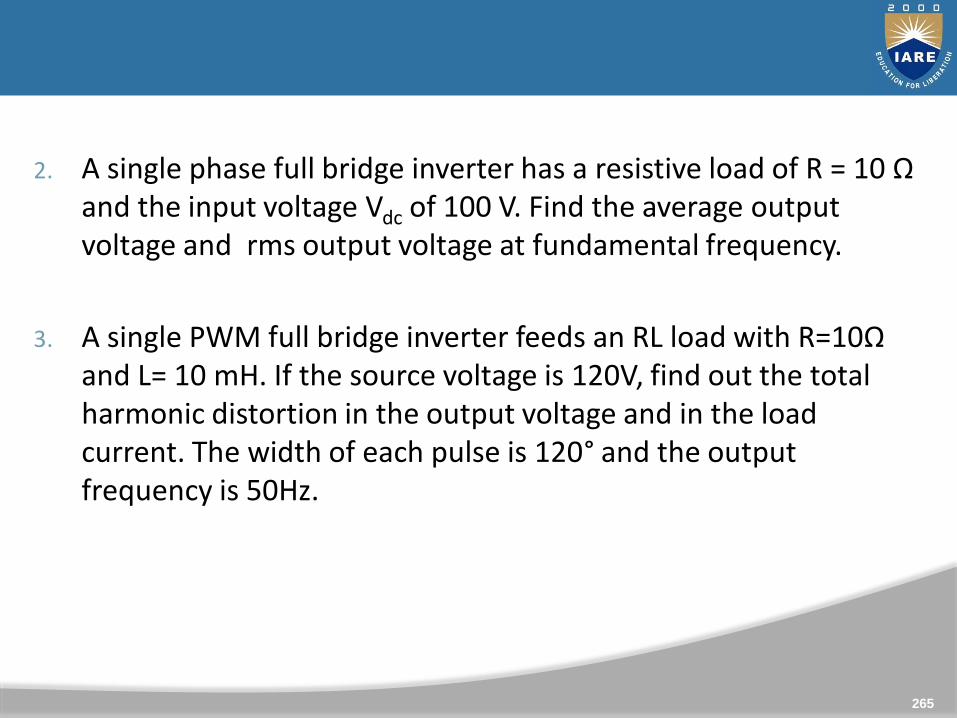
2. A single phase full bridge inverter has a resistive load of R = 10 Ω and the input voltage Vdc of 100 V. Find the average output voltage and rms output voltage at fundamental frequency.
3. A single PWM full bridge inverter feeds an RL load with R=10Ω and L= 10 mH. If the source voltage is 120V, find out the total harmonic distortion in the output voltage and in the load current. The width of each pulse is 120° and the output frequency is 50Hz.
265