Embed Size (px)
Citation preview

1
Introduction to Optoelectronic Devices
Dr. Jing Bai Assistant Professor
Department of Electrical and Computer Engineering
University of Minnesota Duluth
October 30th, 2012
2
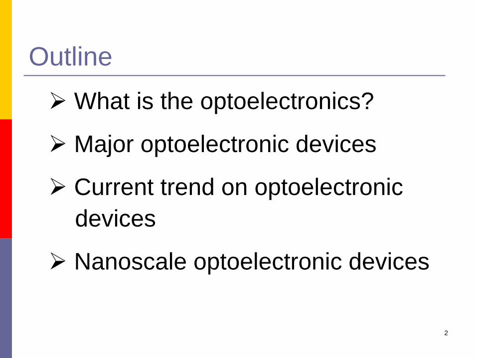
Outline What is the optoelectronics?
Major optoelectronic devices
Current trend on optoelectronic devices
Nanoscale optoelectronic devices
3
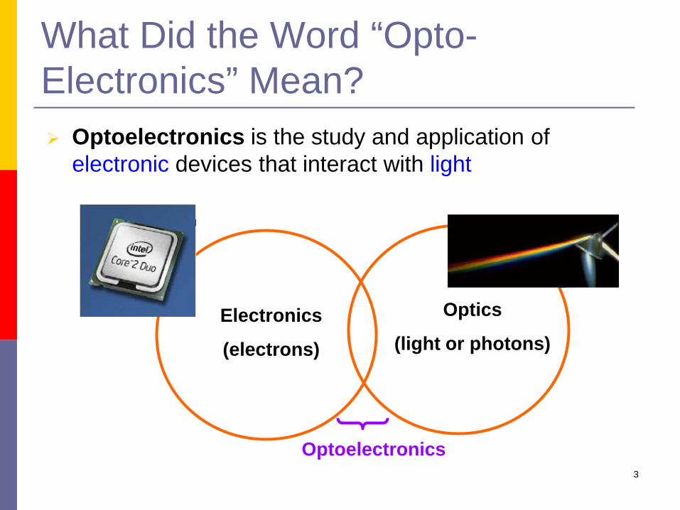
What Did the Word “Opto-Electronics” Mean? Optoelectronics is the study and application of
electronic devices that interact with light
Electronics
(electrons)
Optics
(light or photons)
Optoelectronics

4
Examples of Optoelectronic Devices

5
Light-Emitting Diodes (LEDs)
Light-emitting diode (LED) is a semiconductor diode that emits incoherent light over relatively wide spectral range when electrically biased in the forward direction of the p-n junction.
6
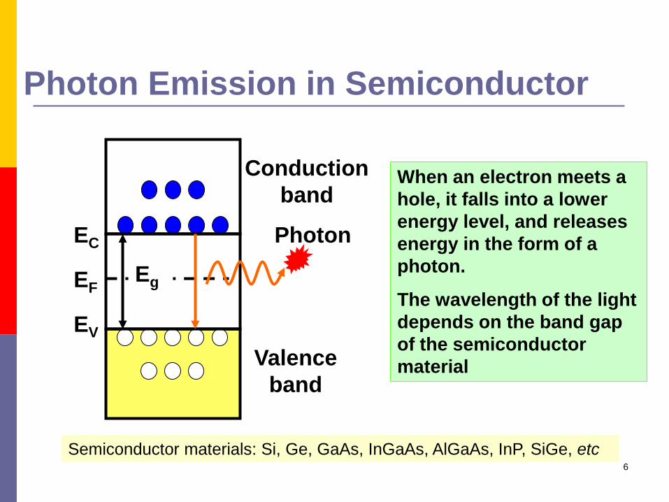
Photon Emission in Semiconductor
EF
EC
EV
Conduction band
Valence band
Photon
Eg
When an electron meets a hole, it falls into a lower energy level, and releases energy in the form of a photon.
The wavelength of the light depends on the band gap of the semiconductor material
Semiconductor materials: Si, Ge, GaAs, InGaAs, AlGaAs, InP, SiGe, etc
7
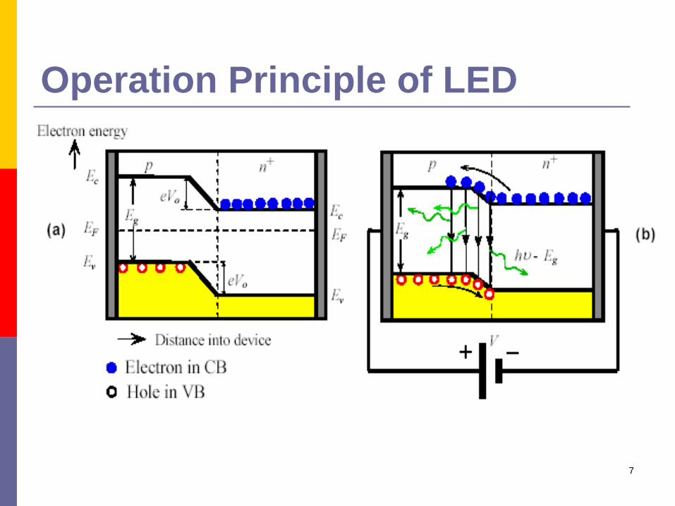
Operation Principle of LED

8
Semiconductor Materials vs. LED Color General Brightness
GaP GaN GaAs GaAIAs --
Green, Red Blue Red, Infrared Red, Infrared --
Super Brightness
GaAIAs GaAsP GaN InGaN GaP
Red Red, Yellow Blue Green Green
Ultra Brightness
GaAIAs InGaAIP GaN InGaN --
Red Red, Yellow, Orange Blue Green --
9
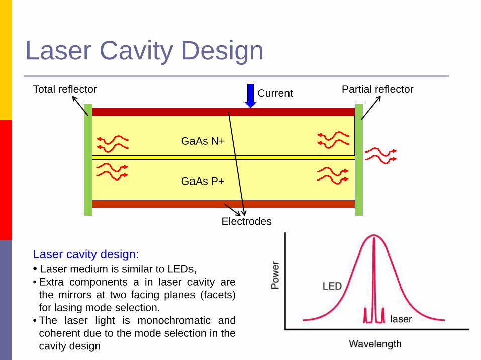
Laser Cavity Design
GaAs N+
GaAs P+
Current Total reflector Partial reflector
Electrodes
Laser cavity design: • Laser medium is similar to LEDs, • Extra components a in laser cavity are
the mirrors at two facing planes (facets) for lasing mode selection.
• The laser light is monochromatic and coherent due to the mode selection in the cavity design

10
Laser Diodes Lasers (Light Amplification by Stimulated Emission)
Photon emission processes:
Absorption Photodetectors
Spontaneous emission LEDs
Stimulated emission Lasers
11
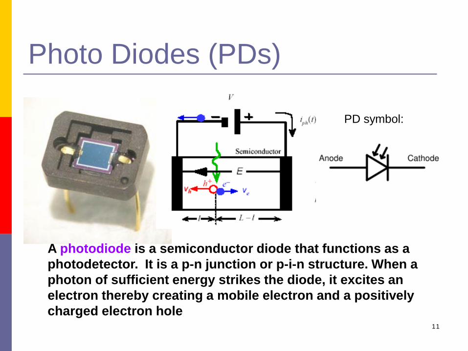
Photo Diodes (PDs)
A photodiode is a semiconductor diode that functions as a photodetector. It is a p-n junction or p-i-n structure. When a photon of sufficient energy strikes the diode, it excites an electron thereby creating a mobile electron and a positively charged electron hole
PD symbol:
12
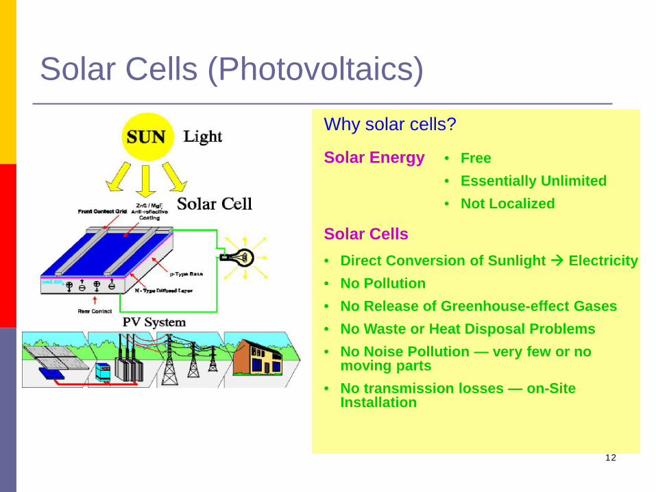
Solar Cells (Photovoltaics)
Solar Energy • Free • Essentially Unlimited • Not Localized
Solar Cells • Direct Conversion of Sunlight Electricity • No Pollution • No Release of Greenhouse-effect Gases • No Waste or Heat Disposal Problems • No Noise Pollution — very few or no
moving parts • No transmission losses — on-Site
Installation
Why solar cells?
13
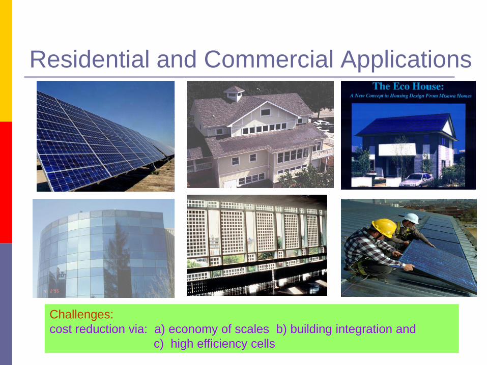
Residential and Commercial Applications
Challenges: cost reduction via: a) economy of scales b) building integration and c) high efficiency cells

14
Solar Energy Spectrum
Spectrum of the solar energy
Solar radiation outside the earth’s surface: 1.35 kW/m2, 6500 times larger than world’s energy demand
AM0: radiation above the earth’s atmosphere AM1.5: radiation at the earth’s surface Blackbody radiation: ideal radiation
15
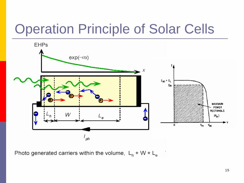
Operation Principle of Solar Cells

16
Trends in optoelectronic devices
Ultra-short, high power mid-infrared light sources
Low cost, easy fabricated materials
Compact multi-wavelength laser sources
Less expensive and high efficiency photovoltaic devices
Molecular and biomedical optoelectronics
— nanoscale optoelectronic devices

17
How Small Is The Nano-Scale?
A human hair is 50,000 – 80,000 nanometers wide and grows ~10 nm every second (~600 nm every minute)
18
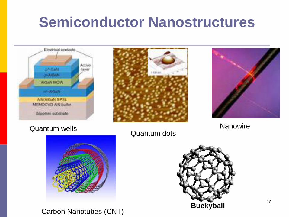
Semiconductor Nanostructures
Quantum dots
Carbon Nanotubes (CNT)
Quantum wells Nanowire
Buckyball
19
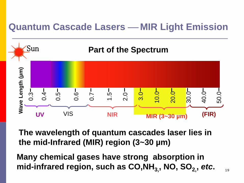
Quantum Cascade Lasers MIR Light Emission
50.0
UV (FIR) VIS NIR
40.0
30.0
20.0
10.
0
3.0
2.0
1.5
0.7
0.3
0.4
0.5
0.6
Wav
e Le
ngth
(µm
)
MIR (3~30 µm)
Part of the Spectrum Sun
The wavelength of quantum cascades laser lies in the mid-Infrared (MIR) region (3~30 µm)
Many chemical gases have strong absorption in mid-infrared region, such as CO,NH3,, NO, SO2,, etc.

20
Quantum-Cascade Laser (QCL)
One electron emits N photons to generate high output power
Typically 20-50 stages make up a single quantum cascade laser
Electric field
ħω
ħω
ħω
Cascade effects
Cross Section of a QCL: Note that the layer thickness is
smaller than the wavelength
10µm
One layer
Dime coin Quantum cascade laser

21
Applications of QCL Environmental sensing and pollution monitoring Automotive
– Combustion control, catalytic converter diagnostics – Collision avoidance radar, cruise control
Medical applications – Breath analysis; early detection of ulcers, lung cancer, etc
QCL for gas detection

22
Challenges in QCL design • Identify various physics interplaying in the QCL cavity and their
effects on pulse propagation • Design Lasing medium for ultra-short, stable, high power MIR
pulse generation for environmental control and biomedical sensing
QCL lasing medium
Time
Power
Input picosecond MIR pulse Output pulse

23
Quantum-Dot Solar Cells
Au grid bar
p+ GaAs substrate
100 nm p GaAs
100 nm n GaAs 30 nm n GaInP
200 nm n+ GaAs
Au contact
Si: GaAs Si: GaAs
Si: GaAs
Si: GaAs 0.5 µm intrinsic region containing
50 layers of quantum dot layers
24
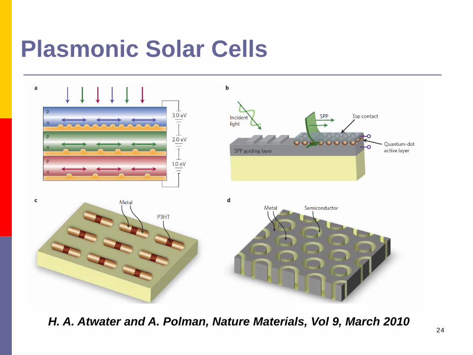
Plasmonic Solar Cells
H. A. Atwater and A. Polman, Nature Materials, Vol 9, March 2010

25
My Contact Information
Email: [email protected] Telephone: (218)726-8606 Office: MWAH 255 Webpage: http://www.d.umn.edu/~jingbai/