Embed Size (px)
Citation preview

LNF Microfluidics workshop 2014
Introduction to Microfluidics
By
Pilar Herrera-Fierro
3/10/2014 LNF Microfluidic Workshop 2014

• Intro to BioMEMS
• Surface properties and modifications
• Soft Lithography
• Making the mold: SU-8 or Si
• metal deposition
• Basic microfluidics design considerations
3/10/2014 LNF Microfluidic Workshop 2014

EECS 509 BioMEMS
What Are MEMS Microsystems?
• Micro Electro Mechanical Systems Are Miniature, Multifunctional Microsystems
Consisting of Sensors, Actuators, and Electronics.
They Are Built Using Micromachining Technologies.
• Micromachining Is an Enabling Technology That
Allows Formation Of Physical, As Well As
Electronic, Devices.
• Micromachining Uses Many of the Standard
Silicon IC Fabrication Techniques.

EECS 509 BioMEMS
Surface-Micromachined Acceleration Sensor (Accelerometer) For
Air Bag Deployment, Manufactured by Analog Devices, Inc.
Photos Courtesy Analog Devices, Inc.
~1
-2m
m
ADXL05:
±5g operating range
1000g survivability
0.5mg/√Hz noise floor
Only a few $!
• Undercut polysilicon shuttle mass
• Differential capacitance sensing
• Force-balanced operation

EECS 509 BioMEMS
BioMEMS
• Implementation of MEMS (Micro Electro Mechanical
Systems) to Bio-related areas
• Fluid delivery system at micro/nano-liter scale
• Multi-physics, multidisciplinary and cross-fields
www.calipertech.com BioMEMS, Lab-on-a-chip

EECS 509 BioMEMS
BioMEMS
• Biomedical MEMS
• Biosensors
• Biotelemetry
• Drug delivery
• Precision surgery
• Minimally-invasive
therapy
• Physical sensors
Deals in vivo with the host
anatomy
• Biotechnological MEMS
• Gene sequencing
• Functional genomics
• Drug discovery
• Pharmacogenomics
• Diagnostics
• Pathogen detection
Deals in vitro with the
biological samples of the
host
Future BioMEMS: Combination of MEMS for in vitro Diagnostics with in vivo Therapy
- Biology Perspective -

EECS 509 BioMEMS
Applications of BioMEMS
Advancement in molecular biology Have brought medical research into molecular level
Advancement in nanotechnology Manipulation of scale in molecular size possible
The applications
- Biological analysis
- Medical diagnosis
- Antigen/Antibody screening
- Chemical analysis and synthesis
- Drug discovery
- Drug screening
- • • • •

EECS 509 BioMEMS
Biomedical Applications of MEMS
Implantable Systems
Functional muscular stimulation (restore limb movement)
Auditory, and Visual Prostheses
Overcome disabilities such as Parkinson and Epilepsy
Pain control, Bladder control, Drug Delivery Systems,
Biological Fluid Analysis Systems
DNA Analysis
Blood Testing/Typing
Chemical/Biological Analysis
Cell-Based Assay Chips
Patient Health Monitoring Measure Patient Health Signs (Activity, breathing, chemistry,…)
Patient Health Service (drug delivery, …)
Environmental Sensing
Air quality
Water quality, and drug dosing
- MEMS & Microsystem Perspective
-

EECS 509 BioMEMS
Courtesy of Prof. Carlos Mastrangelo
THERMAL REACTION
DROP METERING
SAMPLE LOADING
GEL LOADING
SEPARATE DETECT
Integrated DNA Analysis
• Multiple components • Multiple reactions/separations • Decrease size/volume
EECS 509 BioMEMS
Single-Cell Assay Microsystem
Flow direction
Capture site
Captured cell
Actuation membrane
Concentration Generator
Microchamber Selection Logic
Peristaltic Pump
High-throughput Parallel Cell Assay at Single Cell Resolution
- Optimal stem cell culture & transplantation
- Cancer drug screening
Microfluidic Logic Network Microchamber Array for Single-Cells
Prof. E. Yoon, University of Michigan

EECS 509 BioMEMS
Neuro Implants Si based Bio-MEMS applications
Neuro-circuit interaction
Chemical delivery
Issues with long term implant – bio compatibility
Stanford
Robo-hobo: A rat instructed
via a wireless receiver and
brain implant to walk along
a railroad track.
IEEE Spectrum, Aug., 2002

EECS 509 BioMEMS
Drug Delivery Bio MEMS example
Science 2001, MIT
Nature 1999, MIT
http://web.mit.edu/cheme/langerlab/

EECS 509 BioMEMS
Advantages of Microsystems
Small samples
- Nanoliter quantities without evaporative loss
Multiplexing
- Discovery biotech puts a premium on high throughput, enables
genomics, proteomics
Integration, Performance, Speed
- Highly integrated systems possible
- Many analysis method work better as they are scaled down
- Scaling down dramatically improves speed of analysis
Portability (small size), Low reagent and power consumption (low cost)
New types of analysis, new effects to exploit
- Serial chromatographies, dielectrophoresis, surface tension

EECS 509 BioMEMS
Limitations of Microsystems
Techniques dependent on inertia are problematic
- Centrifugation, mixing
Physical state of analytes and carrier solvents can’t change
- Liquid only or gas only systems - solids clog, bubbles unstable and irreproducible
- No precipitation allowed
Interface with macro world
- Reagent reservoirs, sample introduction, detection
Mass transfer rates are tiny
- Mixing generally only occurs by diffusion
Non specific binding - high surface area to volume ratio
Microscale phenomena not fully understood

EECS 509 BioMEMS
Alternative Materials
Materials requirement for BioMEMS is different from those for typical MEMS.
Desired properties of BioMEMS materials
- Biocompatible
- Chemically modifiable
- Surface modifiable
- Easy to fabricate
- Economically viable (cheap… for throw away devices)
- ….
Si, glass and now more toward polymers…
EECS 509 BioMEMS
Types of BioMEMS Devices
Biomaterials
DNA chip cDNA, oligomer
Protein chip Enzyme, antibody, antigen
Cell chip Microorganism, animal cell, neuron
Applications
Bio-electronic device Biocomputing, bio-memory
Implantable chip Prosthetic device, bioinstrumentation
Lab-on-a-chip -TAS, screening
Biosensor Diagnostics, analysis
Microfluidics

EECS 509 BioMEMS
Microfluidics Characteristics
Low Reynolds’s Number, Re
- Laminar flow
- Difficult to mixing
Large surface to volume ratio - Surface effect dominant – bio-surface modification
- Microchannel – pressure drop
Small fluid volume: pL to mL - Nano or micro dispenser
- Diffusion
Fluidic driving - Electroosmotic force
- External pressure force

Surface Properties and Modifications
3/10/2014 LNF Microfluidic Workshop 2014

Hydrophilic vs Hydrophobic Surface
• Hydrophilic: from the Greek (hydros), meaning water, and φιλια
(philia), meaning love.
– Hydrophilic substances can seem to attract water out of the air,
the way salts (which are hydrophilic) do. Sugar, too, is hydrophilic,
and like salt is sometimes used to draw water out of foods.
– A hydrophilic molecule or portion of a molecule is one that is
typically charge-polarized and capable of hydrogen bonding,
enabling it to dissolve more readily in water than in oil or other
hydrophobic solvents.
• Hydrophobic: from the Attic Greek (hydro), meaning water, and
phobos, meaning fear.
– Hydrophobicity is the physical property of a molecule (known as a
hydrophobe) that is repelled from a mass of water.
– Hydrophobic molecules tend to be non-polar and, thus, prefer
other neutral molecules and non-polar solvents.
3/10/2014 LNF Microfluidic Workshop 2014

Contact Angle - Wetting • Contact angle is the angle, conventionally measured through the
liquid, where a liquid/vapor interface meets a solid surface.
• It quantifies the wettability of a solid surface by a liquid via the Young equation.
• A given system of solid, liquid, and vapor at a given temperature and pressure has a unique equilibrium contact angle.
• If the solid–vapor interfacial energy is denoted by gSG, the solid–liquid interfacial energy by gSL, and the liquid–vapor interfacial energy (i.e. the surface tension) by gLG, then the equilibrium contact angle qC is determined from these quantities by Young's Equation:
0 = gSG – gSL + gLGcos qC
3/10/2014 LNF Microfluidic Workshop 2014
Rame-Hart 200 Contact Angle Goniometer
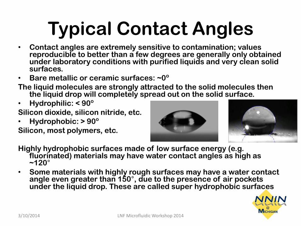
Typical Contact Angles • Contact angles are extremely sensitive to contamination; values
reproducible to better than a few degrees are generally only obtained under laboratory conditions with purified liquids and very clean solid surfaces.
• Bare metallic or ceramic surfaces: ~0o
The liquid molecules are strongly attracted to the solid molecules then the liquid drop will completely spread out on the solid surface.
• Hydrophilic: < 90o
Silicon dioxide, silicon nitride, etc.
• Hydrophobic: > 90o
Silicon, most polymers, etc.
Highly hydrophobic surfaces made of low surface energy (e.g. fluorinated) materials may have water contact angles as high as ~120°
• Some materials with highly rough surfaces may have a water contact angle even greater than 150°, due to the presence of air pockets under the liquid drop. These are called super hydrophobic surfaces
3/10/2014 LNF Microfluidic Workshop 2014

How to Change the Surface Property?
• By coating and patterning a layer of film, you can change the surface property, especially inside a give microfluidic channel.
• Hydrophobic surface formation – By depositing Teflon or SAM (self-assembled monolayer) coating such as FDTS. Also by patterning the surface to customize hydrophobicity.
• Hydrophilic surface formation – By plasma treatment of the surface, you can change the surface from hydrophobic to hydrophilic (e.g. plasma treatment of PDMS). However, the surface property change is typically temporal and its property degrades over time.
3/10/2014 LNF Microfluidic Workshop 2014
Channel Patterning - Superhydrophobicity
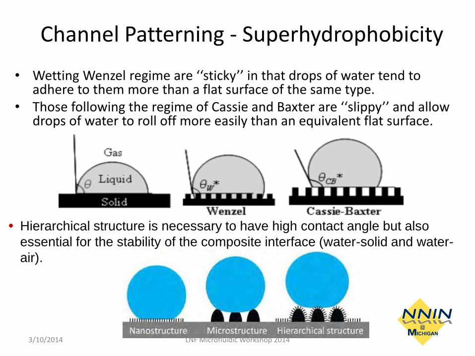
• Wetting Wenzel regime are ‘‘sticky’’ in that drops of water tend to adhere to them more than a flat surface of the same type.
• Those following the regime of Cassie and Baxter are ‘‘slippy’’ and allow drops of water to roll off more easily than an equivalent flat surface.
Hierarchical structure is necessary to have high contact angle but also
essential for the stability of the composite interface (water-solid and water-
air).
3/10/2014 LNF Microfluidic Workshop 2014

Superhydrophobic Surfaces in Biology
• a) Lotus leaf (Nelumbonucifera), b) Hillock bush leaf, (Melaleuca hypericifolia), c) Middle of upper side of a common pond skater (Gerris lacustris), and d) Lichen Lecanora conizaeoides showing high roughness with inset showing water drop WCA 155 +/- 4o. (Source: Soft Matter 2008, 4, 224-240)
3/10/2014 LNF Microfluidic Workshop 2014

Lithographic Surface Modification
• (a) Photolithographic towers, (b) Indented square posts, (c) Diced silicon wafer, (d) Photolithographic towers, (e) Silicon nano-towers, (f) Laser-modified SU8 surface, (g) SU8 towers, (h) Silicon islands and (i) Silicon nanowires grown on those silicon islands. (Source: Soft Matter 2008, 4, 224-240)
3/10/2014 LNF Microfluidic Workshop 2014

PDMS Surface Contact Angle
10l droplets on PDMS hydro-phobic surfaces with droplet contact angles.
100 μm 150 μm
Day 1 Day 6
Growth of a SUM159 sphere shown
over the course of 6 days culture.
White circles outline the growing
SUM159 cells.
1) Silicon wafer 2) Photoresist coating 3) Photolithography
4) Silicon DRIE with
photoresist masking
5) PDMS casting over
the etched silicon
6) PDMS peeling-
off from the silicon
mold
Prof. Euisik Yoon, University of Michigan
(MicroTAS, 2011)
3/10/2014 LNF Microfluidic Workshop 2014

Channel Coating
Hydrophilic microchannel of PDMS and silicon dioxide
Hydrophobic microchannel of PDMS
and FDTS SAM coated silicon surface
Prof. Euisik Yoon, University of Michigan (Biomed Microdevices, 2005) 3/10/2014 LNF Microfluidic Workshop 2014

Capillary Force in Microchannel
• Surface 1: PDMS, Surface 2: SiO2
• Channel can be either hydrophilic or hydrophobic, depending on channel width.
• W > 5m, channel becomes hydrophilic.(Channel depth is 20m.)
Prof. Euisik Yoon, University of Michigan (Biomed Microdevices, 2005) 3/10/2014 LNF Microfluidic Workshop 2014
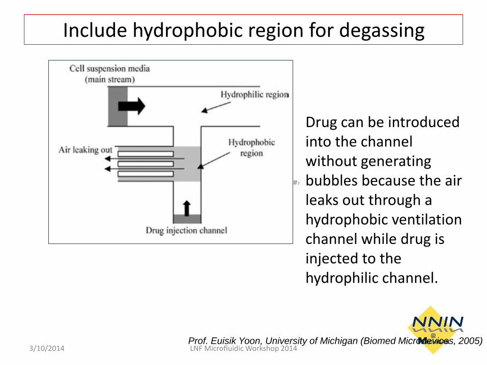
Include hydrophobic region for degassing
Drug can be introduced into the channel without generating bubbles because the air leaks out through a hydrophobic ventilation channel while drug is injected to the hydrophilic channel.
Prof. Euisik Yoon, University of Michigan (Biomed Microdevices, 2005) 3/10/2014 LNF Microfluidic Workshop 2014
Soft Lithography
3/10/2014 LNF Microfluidic Workshop 2014

Photolithography vs. Soft Lithography
Soft lithography
Use of photons for
patterning
(Optical process)
Use of a “soft” (flexible) mold
for patterning
(Physical process)
3/10/2014 LNF Microfluidic Workshop 2014
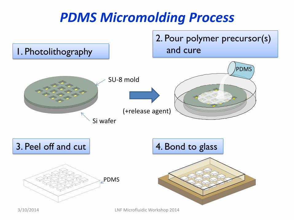
1. Photolithography
2. Pour polymer precursor(s)
and cure
3. Peel off and cut 4. Bond to glass
1.17. PDMS micromolding PDMS Micromolding Process
3/10/2014 LNF Microfluidic Workshop 2014
SU-8 mold
PDMS
Si wafer
PDMS
(+release agent)
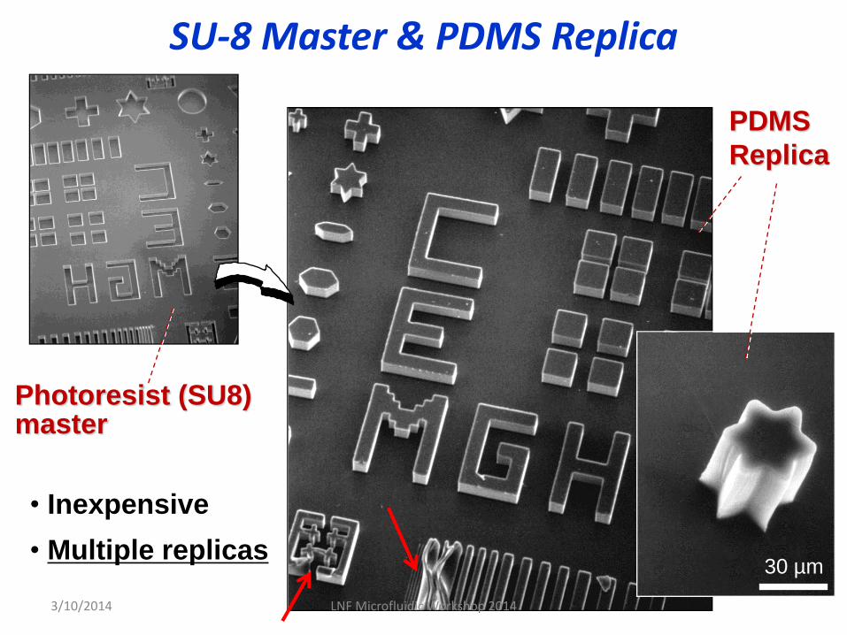
Photoresist (SU8) master
30 µm
PDMS
Replica
• Multiple replicas
• Inexpensive
1.17. PDMS micromolding SU-8 Master & PDMS Replica
3/10/2014 LNF Microfluidic Workshop 2014

Structural integrity of PDMS walls
• Typically, structures with a high aspect ratio (>5:1 height/width)
do not replicate well.
• Some features smaller than 100nm can be replicated.
3/10/2014 LNF Microfluidic Workshop 2014

Structure Collapse of PDMS
• Lateral collapse: Commonly known as “pairing” when H/L > 5 • Sagging: Recessed structure when H/L <0.5
Delamarche, et al., Adv. Mater. (1997)
3/10/2014 LNF Microfluidic Workshop 2014
Remember this when choosing SU-8 type

Polymer with a backbone of Si-O-Si or “siloxane”
Inexpensive
Very elastic and soft
Optically transparent down to 300 nm
Surface is hydrophobic
Self-seals by conformal contact
Inert, but can be oxidized, etched, and derivatized
Biocompatible
Swells when exposed to solvents
High permeability to gases and fluids
Expands a lot with temperature (100 times more than silicon)
Si
O OO
Si
CH3
CH3
CH3
CH3
1.17. The magic of PDMS Properties of PDMS
(Polydimethyl Siloxane)
Two Methyl
Groups on
Silicon
3/10/2014 LNF Microfluidic Workshop 2014

Patterning Techniques Using Soft Lithography
• Replica Molding (REM)
• Micro Contact Printing (CP)
or Microstamping
• Micromolding in Capilaries (MIMIC)
or Microfluidic Patterning
• Microtransfer Molding (TM)
or Stencil Patterning
3/10/2014 LNF Microfluidic Workshop 2014

Replica Molding (REM)
• Additional duplication of pattern transfer from a soft mold
Prof. Whitesides, Harvard (Science 1996) 3/10/2014 LNF Microfluidic Workshop 2014

Microcontact printing (mCP)
1. Ink
2. Transfer
PDMS as a transparent rubber
Material is “added” where stamp contacts
surface
3/10/2014 LNF Microfluidic Workshop 2014

Microfluidic Patterning or Micromolding in capillaries (MIMIC)
1. Fill
2. Remove microchannels
microchannels
Material is added where stamp does not contact the surface
• Immobilization of material
• Procedure for removal of microchannels
• Deposit or etch
3/10/2014 LNF Microfluidic Workshop 2014

Polyurethane Structures on Si/SiO2
• UV-curable polyurathane prepolymer introduced in capillary channels.
• Connected patterns (b), multiple thicknesses mold (c), free standing film after
being dissolved in HF
Prof. Whitesides, Harvard (JACS 1996) 3/10/2014 LNF Microfluidic Workshop 2014

Microfluidically-Patterned Polyurethane 3D
Structures
Or 3D printer?
• Channels filled with UV-curable polyurethane precursor, ant then
exposed to UV to cure the precursor into polyurethane
• Manually stacking 3D structures Prof. Albert Folch, Biomed. Microdevices, 2000
3/10/2014 LNF Microfluidic Workshop 2014

Fabrication of PDMS Stencils MicroTransfer Molding (μTM)
Prof. A. Folch, U. of Washington (Langmuir 2002) 3/10/2014 LNF Microfluidic Workshop 2014

PDMS/PDMS Bonding – sealing channels
• Using Partially Cured PDMS
• Using Uncured PDMS as Adhesive
• Oxygen Plasma
PDMS
Partially-Cured
PDMS
PDMS
PDMS or
Glass
Uncured
PDMS
3/10/2014 LNF Microfluidic Workshop 2014

Oxygen plasma treatment of PDMS
• Reactive oxygen radicals (O+) attack methyl groups (Si-CH3) on the surface.
• Condensation reaction between silanol groups (Si-O-H) will form siloxane (Si-O-Si) to bond two PDMS layers.
3/10/2014 LNF Microfluidic Workshop 2014
Will
bind to
glass

Multi-Level Microfluidic Channels
M. Zhang, Lab Chip 2010 3/10/2014 LNF Microfluidic Workshop 2014

Fabricated Tactile Sensor Module
Electrode
Spacer
22mm 22mm
Bump
1mm
Air channel
Prof. E. Yoon, JMEMS 2006 3/10/2014 LNF Microfluidic Workshop 2014

Fabricated Tactile Sensor Module
Electrode
Spacer
22mm 22mm
Bump
1mm
Air channel
3/10/2014 LNF Microfluidic Workshop 2014

SU-8 Mold fabrication
3/10/2014 LNF Microfluidic Workshop 2014

Silicon - Si • Semiconductor, group IV
• Diamond Lattice unit cell
• Each atom shares its 4 valence electrons with 4
neighboring atoms
• There are 5x10²² atoms/cm3 in the Si lattice
• The crystalline nature of Si influences many of
its properties
From Fundamentals of Microfabrication by M. Madou
Tetrahedral Bonding of Si
Face-Centered
Cubic (FCC) unit cell Diamond Lattice
3/10/2014 LNF Microfluidic Workshop 2014

Miller Indices for a Simple Cubic Structure
• (xyz) values are the inverse of the coordinate of the intercepts of a given plane with the three axes;
• For example (100) represents the plane that intersects the x axis and runs parallel to the yz plane.
• [xyz] is a given crystal direction and represents the direction of the vector perpendicular to the plane (100).
• As we will see later, properties of Si change along these different planes.
x
y
z
1
1
1 x
(xyz)
(100)
Plane y
z
1
1
1 x
(110) Plane y
z
1
1
1
(111) Plane
<100> Direction
<110> Direction
<111> Direction
3/10/2014 LNF Microfluidic Workshop 2014
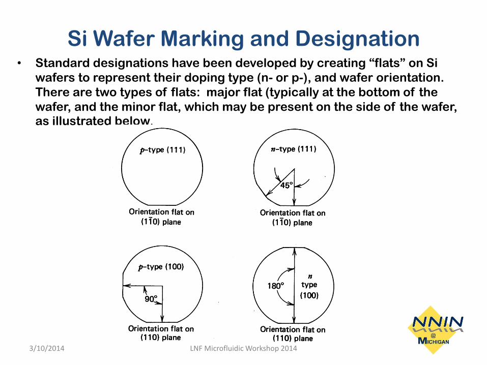
Si Wafer Marking and Designation • Standard designations have been developed by creating “flats” on Si
wafers to represent their doping type (n- or p-), and wafer orientation.
There are two types of flats: major flat (typically at the bottom of the
wafer, and the minor flat, which may be present on the side of the wafer, as illustrated below.
3/10/2014 LNF Microfluidic Workshop 2014

Why Do We Care About Orientation?
Create a pattern in a mask on a (100) wafer. The
mask edge (assume rectangular shape) is
aligned to the <110> direction. (100)
If the etch proceeds for a long time,
the 4 {111} planes meet in an
inverted pyramid shape.
(111)
Planes
54.7
° Slight undercutting
under the mask
(100)
Surface
Because (111) planes etch much slower, the
etch front practically stops on these planes,
while other planes continue to etch.
<110>
3/10/2014 LNF Microfluidic Workshop 2014

Photolithography how to make the SU-8 mold
• The process of printing a given 2D pattern onto a thin film layer
• This is a photographic process that requires a photosensitive material
“photoresist”, and a “mask” that permits exposure of only defined
regions to the incident radiation
• The mask:
– Typically made of a glass plate (soda lime or quartz glass) that is
transparent to UV light
– The pattern of interest is created on the glass using a thin (<1µm)
metal film such as chromium (Cr) or gold (Au)
– The mask plate has the pattern of interest repeatedly printed on it.
– Mask polarity can be designed to either allow incident radiation
pass through the patterned regions (i.e., dark field), or pass through
the field regions outside of the patterned areas (I.e., clear field)
Pattern of Interest
Pattern Generation
(PG) Pattern repeated on a glass plate
Step &
Repeat
3/10/2014 LNF Microfluidic Workshop 2014

• The photoresist (PR) : – A polymer whose chemical properties change when it is exposed to incident
radiation, typically UV light. Note that PR cannot be exposed to temperatures above about 200°C because it burns (note that this is a polymer like plastic).
– The PR can be then developed in a “developer” like the standard photographic process;
– Two different results can be obtained depending on the type of PR used: • Positive PR: This type of PR is removed (etched away) in the developer solution only in areas
that have been exposed to UV radiation • Negative PR: This type of PR is hardened (and therefore cannot be removed) in the developer
solution in areas that have been exposed to UV radiation.
– PR is typically in liquid form that can be spun onto a silicon wafer at speeds of a few thousand RPM’s. This spinning process creates a uniform film thickness in the range of 1-100’s of microns.
– After application, the PR is baked at 90-100°C to remove the solvents – The PR is now ready to be exposed and developed.
Photolithography
3/10/2014 LNF Microfluidic Workshop 2014
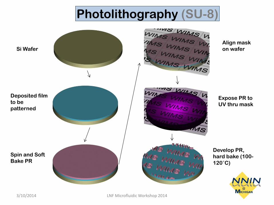
Photolithography (SU-8)
Si Wafer
Deposited film
to be
patterned
Spin and Soft
Bake PR
Align mask
on wafer
Expose PR to
UV thru mask
Develop PR,
hard bake (100-
120°C)
3/10/2014 LNF Microfluidic Workshop 2014

Photolithography: Positive vs. Negative PR (SU-8)
Clear-Field Mask Dark-Field Mask
Positive PR’s are typically used because they are easier to work with and use
less corrosive developers and chemicals
+ve PR +ve PR -ve PR
3/10/2014 LNF Microfluidic Workshop 2014

Tilted Exposure
Prof. S. Lee, KAIST (JMM 2007) 3/10/2014 LNF Microfluidic Workshop 2014

Maskless Photolithography
Direct Laser Writing • Raster Scanning of SU8
Courtesy of Prof. Alber Folch, University of Washington
3/10/2014 LNF Microfluidic Workshop 2014
• Also known as greyscale
• Heidelberg Micro PG 501
• 2micron min feature
• Fast writing

• The material to be deposited is placed in a vacuum chamber, it is somehow heated so it melts and evaporates. The vapor phase molecules land on the target wafer and form a thin film.
• Two basic approaches to evaporation are:
– Thermal Evaporation
– Electron-beam (E-beam) evaporation
• Thermal evaporation is the easiest of all and requires the simplest system. The film to be deposited is placed inside a crucible inside a vacuum chamber. The crucible is heated until the material evaporates.
• Heating of the crucible can be done in several ways, including resistive and inductive heating.
• The temperature required to evaporate the material depends on the vapor pressure of the material and on the pressure.
• Typically the material should have a vapor pressure of more than 10mTorr.
• The pressure in the chamber typically ranges from 0.1-1 µTorr
• Vapor pressure of different materials is shown on the next page.
Thin Film deposition (contacts)
Physical Vapor Deposition: Evaporation
3/10/2014 LNF Microfluidic Workshop 2014

• In e-beam evaporation, the material is heated and melted using a high-energy electron beam.
• With e-beam, higher temperatures can be achieved. Therefore, a wider range of materials can be deposited.
• Because of the higher temperatures possible with e-beam, in addition to refractory metals with low vapor pressure, it is possible to deposit some insulators such as oxides and glass.
• The evaporation rate is higher at lower pressures.
• Since the crucible is not heated as much, there is less contamination possibility using e-beam evaporation than thermal evaporation.
• Most materials used in the IC industry these days, use e-beam evaporation.
• Evaporation in general does not have a very good step coverage and the process is “line of sight”, as illustrated below.
Physical Vapor Deposition: Evaporation
Si Thinner (or discontinuous)
Film On Edge
Deposited Film Arriving Atoms
3/10/2014 LNF Microfluidic Workshop 2014

• A plasma is generated by applying a RF signal 5-15kV in a pressure range of 10-100 mTorr.
The gas used is typically Ar.
• The plasma creates Ar ions and electrons.
• Ar ions bombard the source knocking off source atoms.
• The source atoms get deposited on the substrate (target).
• Features:
– Wide variety of materials, including metals, insulators, and semiconductors
– When deposited in a reactive environment with oxygen, oxides can be deposited
– One can deposit multiple materials in a single pump down (meaning we do not need to
break vacuum for next material) since multiple sources can be placed in the same
chamber. It is also possible to deposit alloys and compounds like silicides (MoSi, TaSi)
– The films are deposited with better step coverage than e-beam so there is film continuity
going over steps.
Physical Vapor Deposition: Sputtering
+
-
RF Source
13.56MHz
Target
Wafer
Source
Plasma
Vac
uu
m
3/10/2014 LNF Microfluidic Workshop 2014

Thin Film Issues
• Adhesion
• Diffusion Barrier/Interface
• Ohmic Contacts
• Step Coverage
• Electromigraion
• Stresses
3/10/2014 LNF Microfluidic Workshop 2014

Isotropic Wet Silicon Etching (ISE)
• Si can be etched isotropically (equal etch rate in all directions) in a mixture of HF+HNO3, and some acetic (vinegar) acid (this mixture is sometimes referred to as HNA) This etch was developed in the 1960’s as the solid-state circuits industry was working on the development of beam-lead technology for building high-density circuits.
• The etch removes n- or p-type silicon in all directions at about the same rate.
• The etch does depend on agitation. The more agitation there is during the etch the larger the undercut under the masked regions.
• The etch attacks most materials (HF is nasty acid that attacks many materials). For shallow etches, silicon nitride can be used as a mask, for deep etches sometimes it is required to use Cr/Au. HF does not significantly attack silicon directly but the HF+HNO3 mixture is a strong etchant of Si.
Si substrate
With No Agitation
Mask
(usually nitride)
Si substrate
With Agitation
3/10/2014 LNF Microfluidic Workshop 2014
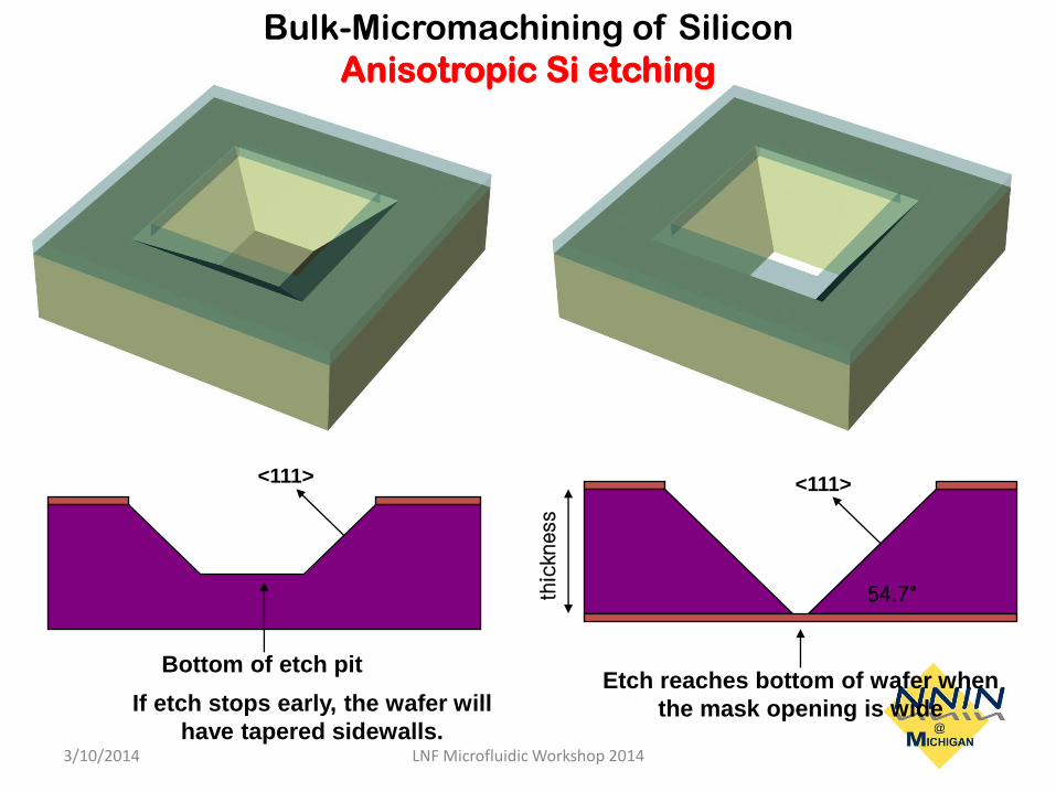
Bulk-Micromachining of Silicon
Anisotropic Si etching
<111>
Bottom of etch pit
If etch stops early, the wafer will
have tapered sidewalls.
Etch reaches bottom of wafer when
the mask opening is wide
<111>
54.7° thic
kness
3/10/2014 LNF Microfluidic Workshop 2014

Dry (Plasma) Etching • Dry etching is also a chemical etching technique, but employs gases instead of liquids. The gases
are ionized in an RF glow discharge (plasma) and the specific chemical species are used to etch the thin film.
• The gases used to create the plasma determine the etch rate, etch profile, and selectivity. Many gases are used to etch different thin films. A few of them, and the material they can etch are listed below.
• One of the main disadvantages of dry (plasma) etching is the worse selectivity it has with respect to both the mask (typically PR), and to different layers.
• Dry etching is now very
commonplace.
Plasma
Wafers
Chamber
RF
Power
Material Etch Gas
Si/Poly-Si CF4, SF6, ..
SiO2 CHF3, CF4/H2, CF4/O2
Si3N4 CF4/O2
Organics O2, O2/CF4, O2/SF6
Al BCl3
3/10/2014 LNF Microfluidic Workshop 2014

EECS 509 BioMEMS 67
Bulk Micromachined Silicon Microchannels
Chen and Wise,
Transducers 1995
Tjerkstra, et al., MEMS 1997

EECS 509 BioMEMS 68
Micro-Fluidic Channel – Design considerations
Microfluidics: Dimension < 1 mm
Nanofluidics: Dimension < 1 mm
Newtonian fluid (applying Navier-Stokes Equation) - Coefficient of viscosity is constant over all shear stress
- Incompressible, Steady (time-invariant) flow
- Fully developed flow
Laminar flow due to low Reynolds number - No turbulence Mixing becomes difficult
Priming bubbles very difficult - Surface tension > buoyant force
Capillary and viscous forces become dominant.
Electrophoretic, Electroosmotic flows more easily handled than pressure driven flow.

EECS 509 BioMEMS 69
Reynolds Number
Ratio of the inertial force to the viscous force
Turbulent flow : unsteady flow
Laminar flow : steady flow
Transitional value (Re): 2,000~3,000
cm)(g/sec viscosity:
ter)(4A/perimediameter hydraulic :channel of area sectional-cross :A
rate flow c volumatri:
density :
Re
hD
Q
hDA
Qh
vD

EECS 509 BioMEMS 70
Mechanism of Mixing
Mixing was produced by mechanical and molecular
physical process
Macro-scale: Dominated by mechanical process
- Turbulence, stirring
Micro-scale: Dominated by molecular process
- Laminar, diffusion

EECS 509 BioMEMS 71
Fabrication of Microfluidic Channels - Summary
Silicon and Glass
- Conventional micromachining, bonding, etching
- Expensive
Plastics
- Injection molding using thermoplastic materials such as
polystyrene, polypropylene, etc.
- Inexpensive
PDMS
- Good research material but not amenable to inexpensive mass
production for commercial devices.
Hydrogels
- Highly porous polymeric matrices: collagen, Matriegel, agarose,
PED, etc.; Easily molded from a PDMS mold for 3D cell culture.
Paper
- Extremely inexpensive, natural embedded capillary pump

EECS 509 BioMEMS 72
See you in the lab


![Advances in Microfluidics‐Based Assisted Reproductive ... · microfluidics has also been used for 3D cell culture and cryo-preservation.[12] Furthermore, droplet-based microfluidics](https://img.pdfslide.us/doc/110x75/5e831de01be17b7cdc733cfb/advances-in-microfluidicsabased-assisted-reproductive-microfluidics-has-also.jpg)