Embed Size (px)
Citation preview

Introduction to LTspice
ReadMeFirst
Lab Summary
In this lab, you will be using a SPICE simulator known as LTspice. SPICE (Simulation Program
with Integrated Circuit Emphasis) is a general-purpose, open source analog electronic circuit
simulator. It is a program used in integrated circuit and board-level design to check the integrity
of circuit designs and to predict circuit behavior.
The three different analyses that will be performed in this lab are DC Operating Point Analysis,
Transient Analysis and AC analysis.
Lab Preparation
Files:
LTspice_Shortcuts.pdf

Part 1 – Introduction
Open LTspice by clicking on the shortcut found on your desktop. Once the program is
open, create a new schematic by clicking on the “New Schematic” icon on the toolbar.
Once the schematic is created, click on “File” and “Save as” and save the new schematic as “DC
OP Analysis”. Start by adding a resistor to your new schematic. This can be done by either using
the shortcut “R” or by clicking on the resistor icon in the toolbar. Once the resistor is
selected you can rotate the component by pressing “Ctrl+R”. Left-click once to place the
resistor on the schematic. You can press “Esc” on your keyboard once you’re done placing the
resistor. You can move around your schematic by holding left-click and dragging the mouse
anywhere on your schematic. You can zoom in and out of your schematic using the mouse’s
scroll wheel or by using the icons on the toolbar. If you ever zoom out too much
you can click on the “Zoom Full Extents” icon (Spacebar or ) to zoom to fit your schematic.
The move icon (F7 or ) will allow you to freely move components around your schematic
while the drag icon (F8 or ) drags the components and any wires that may be connected to
it. In order to move multiple components at once, click on the move icon and select the
components or wires that you want to move by holding left-click and dragging the cursor over
the components you want to move. The same procedure can be done using drag.
A list of useful shortcuts are available in the LTspice_Shortcuts document on the lab website.

Part 2 – DC Operating Point Analysis
DC Operating Point Analysis calculates the behavior of a circuit when a DC voltage or current is
applied to it. The result of this analysis is generally referred as the bias point or quiescent point,
Q-point.
We will be building the same resistor network that we analyzed in the Resistor Networks lab for
our DC analysis. Using the same schematic that you created earlier, place 6 resistors on your
schematic like in the screenshot below.
Figure 1 Inserting components on schematic

Now add a voltage source by clicking on the components icon (F2 or ) and selecting
“voltage” from the menu as seen below.
Figure 2 Selecting Voltage Source
Connect the components using the wire tool (F3 or ) as seen below.
Add the ground (G or ) to the schematic as well.
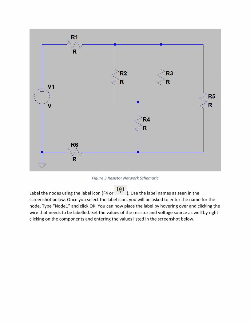
Figure 3 Resistor Network Schematic
Label the nodes using the label icon (F4 or ). Use the label names as seen in the
screenshot below. Once you select the label icon, you will be asked to enter the name for the
node. Type “Node1” and click OK. You can now place the label by hovering over and clicking the
wire that needs to be labelled. Set the values of the resistor and voltage source as well by right
clicking on the components and entering the values listed in the screenshot below.

Figure 4 Resistor Network Schematic with Net names
You are now ready to run the DC Operating Point Analysis. Click on the Simulation icon ( )
and select the “DC op pnt” tab and click OK. A window will then pop up showing the voltage at
the various nodes and the current through the source and the resistors like in the screenshot
shown below. (Note that most of the values in the screenshot are hidden)
Figure 5 Operating Point Simulation Results

Although it makes sense for the current through the source (V1) to be negative, you may
observe that some resistors have a negative current flowing through them as well. This can be
fixed by moving that resistor and rotating it twice and putting it back to its place. If you rerun
the simulation, you will observe that the current flowing through that resistor is now positive.
Keep in mind that passive resistors do not work this way in the real world and that the direction
of the resistor doesn’t affect the polarity of the current.
Record the voltage and current values in the results sheet.
After running the simulation, you can also view the voltage at each node by simply clicking on
the node. You can then right-click on the voltage value and modify it to show a different value
such as current by selecting the value from the “Displayed Data” window. (Just be sure to
remove the ‘$’ sign which usually aliases to the node voltage you selected) You can also display
your own equations, for example, you can display the power consumed by resistor R2 by typing
in the expression, “ (V(output)-V(node1))*I(R2) “.
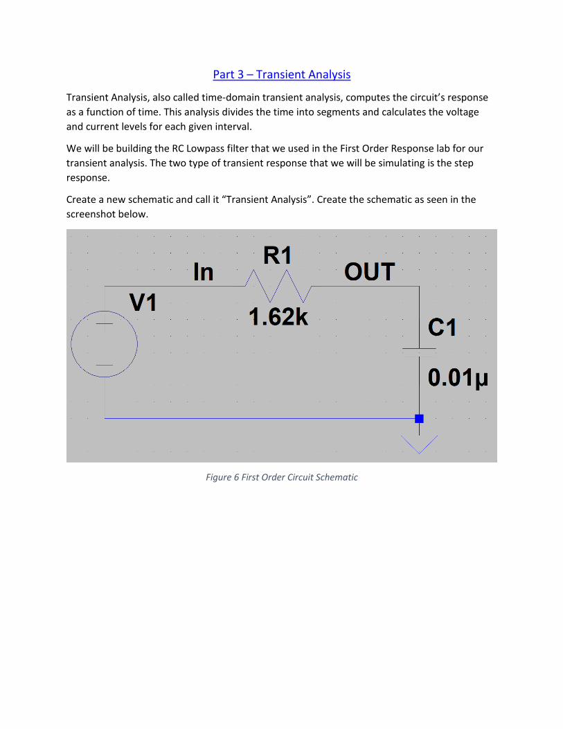
Part 3 – Transient Analysis
Transient Analysis, also called time-domain transient analysis, computes the circuit’s response
as a function of time. This analysis divides the time into segments and calculates the voltage
and current levels for each given interval.
We will be building the RC Lowpass filter that we used in the First Order Response lab for our
transient analysis. The two type of transient response that we will be simulating is the step
response.
Create a new schematic and call it “Transient Analysis”. Create the schematic as seen in the
screenshot below.
Figure 6 First Order Circuit Schematic

Set the voltage source to be a pulsed function by right-clicking it and selecting “Advanced”.
Select “PULSE” under Functions and set the parameters to the values shown in the screenshot
below.
Figure 7 Voltage Source Advanced Settings
The above parameters should create a square wave with a 50% duty cycle at a frequency of 1
KHz and an amplitude of 5 Vp-p. You are now ready to run the transient analysis. Click on the
Run icon. Under the Transient Analysis tab, set the stop time to 0.002 (or 2m) seconds and click
ok. Once the simulation is done, hover over the schematic and select the output (Out) and
input (In) nodes using the probe cursor. You should now be able to see the graph for the step
response similar to the one shown below. (Note that the font size and colors were modified to
make the graph more visible)

Figure 8 Transient Analysis Graph
To zoom in to a certain area of the graph, hold left-click and highlight the desired area. You can
zoom to fit your graph by simply right-clicking anywhere on the graph and selecting “Zoom to
Fit”.
We will now measure the time constant from the simulation similar to what was done in the
First Order Response lab. Since we only need the output trace for this, right-click “V(In)” and
select “Delete this Trace”. Cursors can be placed on the graph by clicking on the corresponding
title. Bring up two cursors on the output by clicking V(out) twice. Measure the Decay time by
placing one cursor at the start of the decay and the other cursor halfway (2.5 V) and record the
Difference in the Horizontal value in the Cursor pop-up window. To set the cursor close to 2.5 V,
you will need to zoom in to the graph at 2.500 V in order to increase the resolution. Once
zoomed-in it will be easier to drag the cursor to the desired value. The cursor seen in the
screenshot below was set close to 2.5 V this way.

Figure 9 Transient Analysis Graph Zoomed In
Calculate the time constant from the measured decay time and enter your answer in the results
sheet. If you forgot how to calculate the time constant, refer back to the First Order Response
Screencast.

Part 4 – DC Sweep Analysis
DC Sweep Analysis is used to calculate a circuits’ bias point over a range of values. This
procedure allows you to simulate a circuit many times, sweeping the DC values within a
predetermined range. You can control the source values by choosing the start and stop values
and the increment for the DC range. The bias point of the circuit is calculated for each value of
the sweep.
For this simulation, we will use the non-inverting the Operational Amplifier (Op-amp)
configuration we used in the Operational Amplifiers 1 lab.
In order to use the LME49710 SPICE model, the model and symbol file must be added to the
appropriate folders. Download the LME49710.lib and LME49710.asy files from the lab website.
Paste the LME49710.lib file under “This PC -> Documents -> LTspiceXVII -> lib -> sub” and paste
the LME49710.asy file under “This PC -> Documents -> LTspiceXVII -> lib -> sym -> Opamps”.
Note: Once the files are placed in those folders you may need to restart LTspice in order to be
able to see the LME49710 Op-amp under Components.
Create a new schematic and call it “DC Sweep Analysis”. Open components (F2 or ) and go
to [Opamps] and select the LME49710 Op-amp. Place the Op-amp in the schematic and build
the schematic seen in the screenshot below.
Figure 10 Non-Inverting Operational Amplifier Schematic
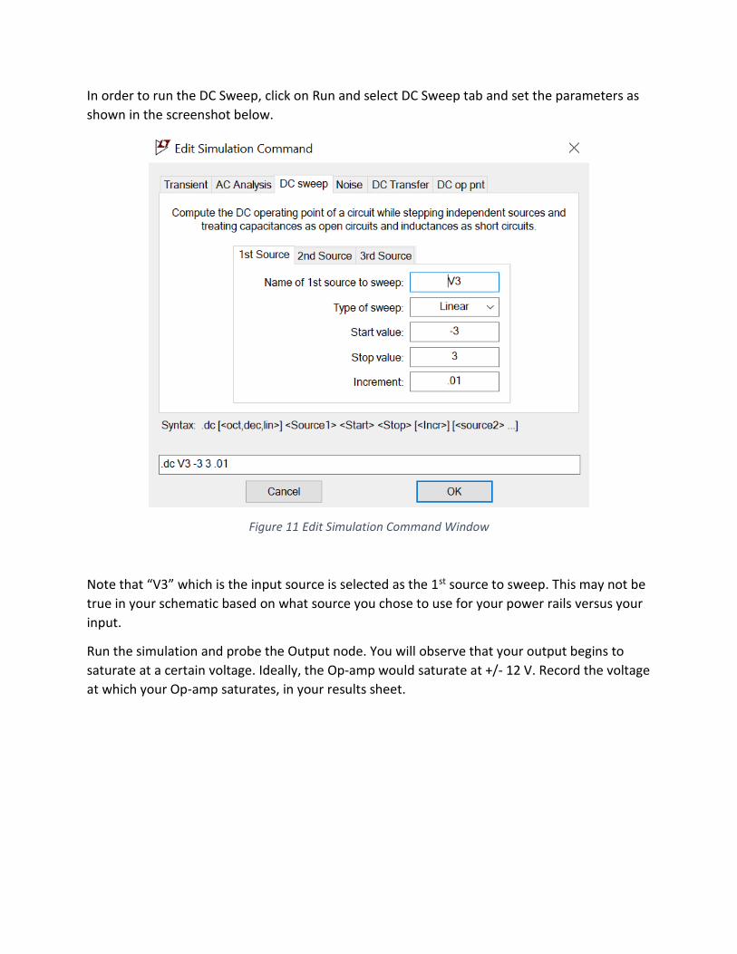
In order to run the DC Sweep, click on Run and select DC Sweep tab and set the parameters as
shown in the screenshot below.
Figure 11 Edit Simulation Command Window
Note that “V3” which is the input source is selected as the 1st source to sweep. This may not be
true in your schematic based on what source you chose to use for your power rails versus your
input.
Run the simulation and probe the Output node. You will observe that your output begins to
saturate at a certain voltage. Ideally, the Op-amp would saturate at +/- 12 V. Record the voltage
at which your Op-amp saturates, in your results sheet.

Part 5 – AC Analysis
AC Analysis is used to calculate the small-signal response of a circuit. In AC Analysis, the DC
operating point is first calculated to obtain linear, small-signal models for all nonlinear
components. Then, the equivalent circuit is analyzed from a start to a stop frequency. The
result of an AC Analysis is displayed in two parts: gain versus frequency and phase versus
frequency.
For this simulation, we will use the same non-inverting the Op-amp configuration we used in
the previous section. Go back to your old “DC Sweep Analysis” schematic and save as “AC
Analysis”. Set your input source to have an AC amplitude of 1 by right-clicking on your source
and “Advanced” as seen in the screenshot below.
Figure 12 Voltage Source Advanced Settings

In order to modify or change the type of simulation from DC Sweep to AC analysis, you can go
to Simulate -> Edit Simulation cmd or by simply right-clicking the DC Sweep spice directive line
on the schematic. Select the AC analysis tab and set the parameters as shown below.
Figure 13 Edit Simulation Command Window
Run the simulation and select the Output node. Use the cursors to find the cutoff frequency.
Record the DC gain (V/V) and frequency at the cutoff. Calculate the Gain-Bandwidth Product
(GBWP).
If you forgot how to measure the cutoff frequency and how to calculate the GBWP, refer back
to the Operational Amplifiers 1 Screencast.
*** END of LAB ***