Embed Size (px)
Citation preview
Introduction to FPGA Design
Illustrating the FPGA design process using Quartus II design software and the Cyclone II
FPGA Starter Board.
Physics 536 – Spring 2009

Why FPGA’s?• Digital logic:
– Equivalent to a large number of discrete logic elements– NOT a microprocessor (although microprocessors can be
implemented in an FPGA design)
• High density:– All the logic is inside a single chip– No need for interconnecting traces on PCB between logic
circuits
• Reprogrammable:– Designs can be changed after the hardware has been
manufactured– High-level design software optimizes the usage of limited
resources

FPGA Resources
• Both companies produce competitive products – neither is endorsed. Other companies exist...
• We use Altera tools to demonstrate the design process.
• Xilinx has a similar set of tools.• Conceptually, the design process is the same.
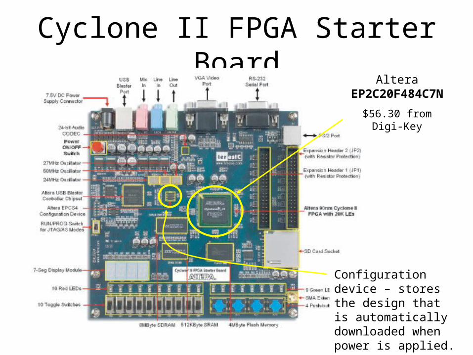
Cyclone II FPGA Starter BoardAltera
EP2C20F484C7N
$56.30 from Digi-Key
Configuration device – stores the design that is automatically downloaded when power is applied.
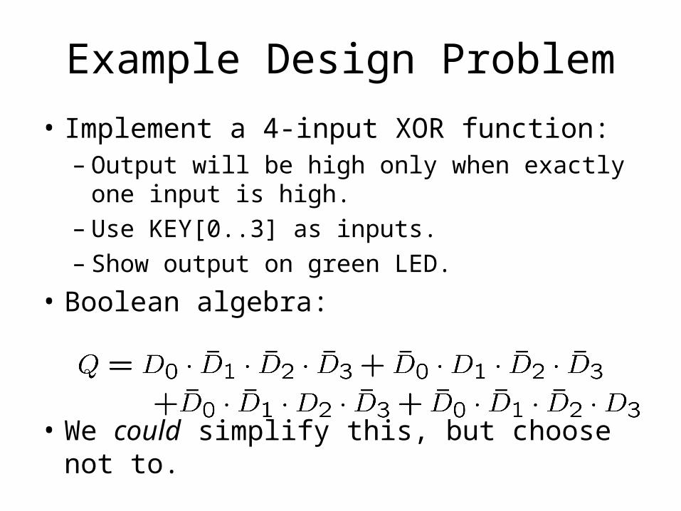
Example Design Problem
• Implement a 4-input XOR function:– Output will be high only when exactly one
input is high.– Use KEY[0..3] as inputs.– Show output on green LED.
• Boolean algebra:
• We could simplify this, but choose not to.
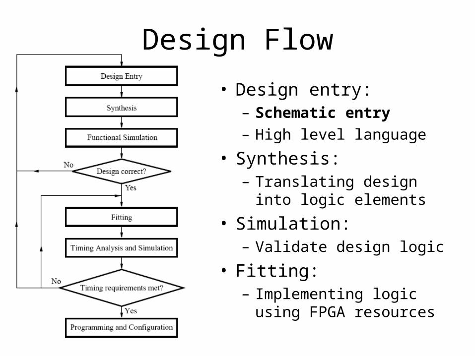
Design Flow
• Design entry:– Schematic entry– High level language
• Synthesis:– Translating design into
logic elements
• Simulation:– Validate design logic
• Fitting:– Implementing logic using
FPGA resources
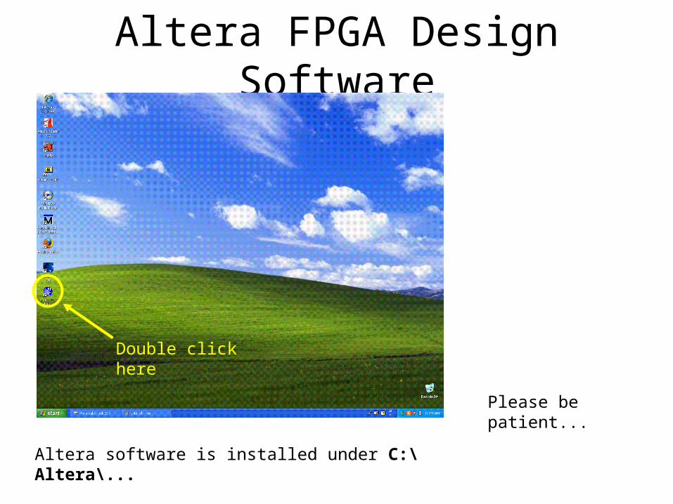
Altera FPGA Design Software
Double click here
Altera software is installed under C:\Altera\...
Please be patient...
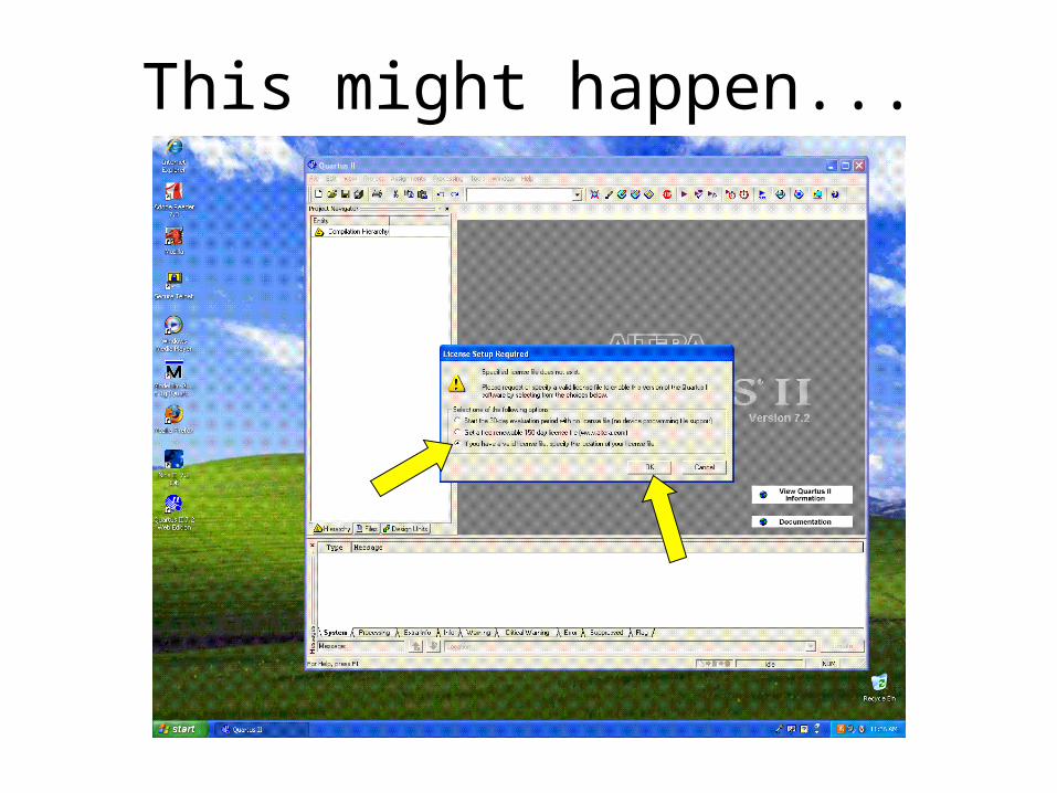
This might happen...
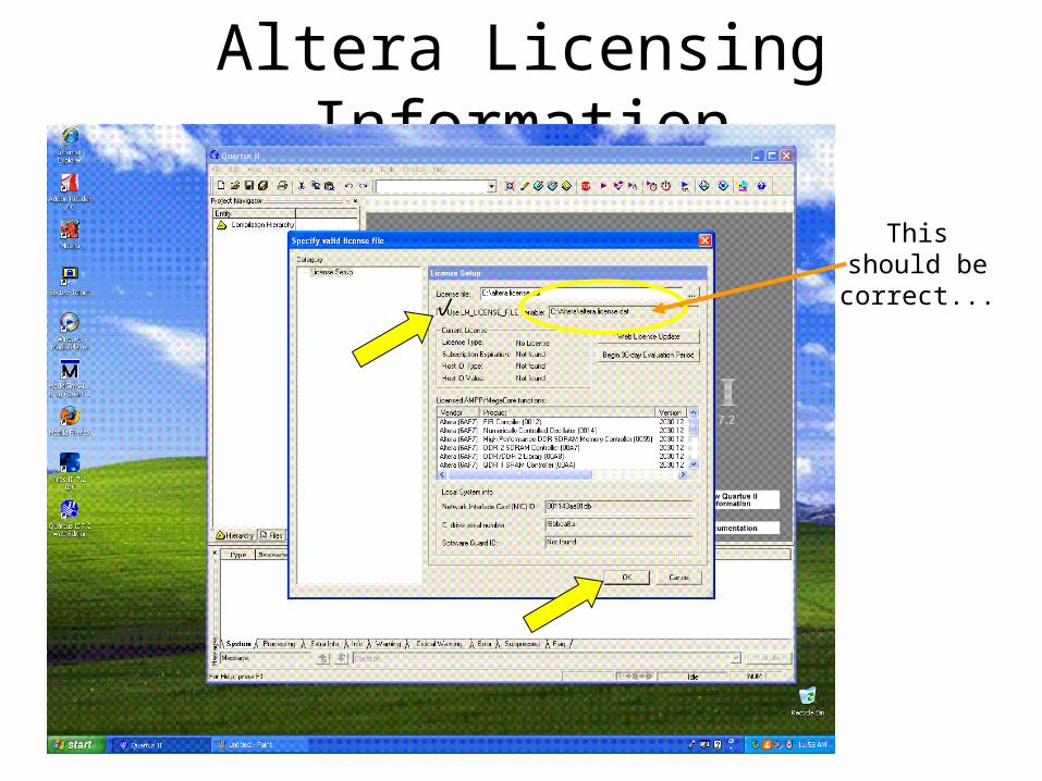
Altera Licensing Information
This should be correct...
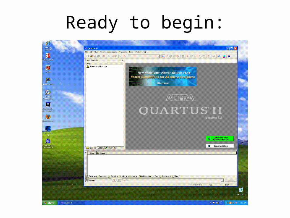
Ready to begin:
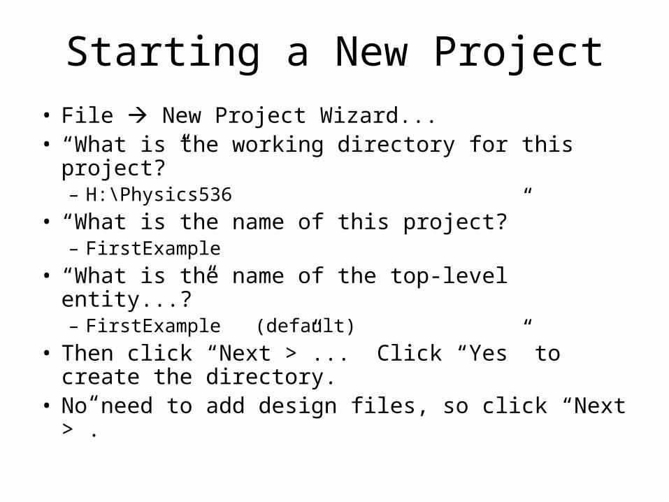
Starting a New Project
• File New Project Wizard...• “What is the working directory for this project?”
– H:\Physics536
• “What is the name of this project?”– FirstExample
• “What is the name of the top-level entity...?”– FirstExample (default)
• Then click “Next >”... Click “Yes” to create the directory.
• No need to add design files, so click “Next >”.
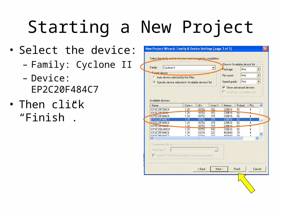
Starting a New Project• Select the device:
– Family: Cyclone II– Device: EP2C20F484C7
• Then click “Finish”.
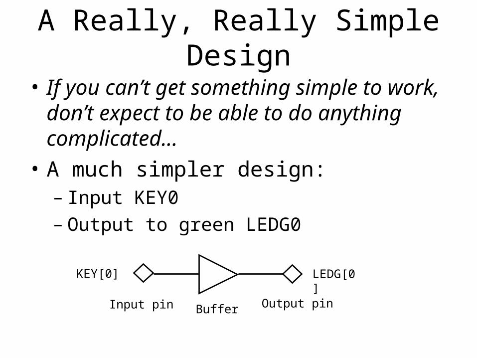
A Really, Really Simple Design
• If you can’t get something simple to work, don’t expect to be able to do anything complicated...
• A much simpler design:– Input KEY0– Output to green LEDG0
KEY[0] LEDG[0]
Input pin Output pinBuffer
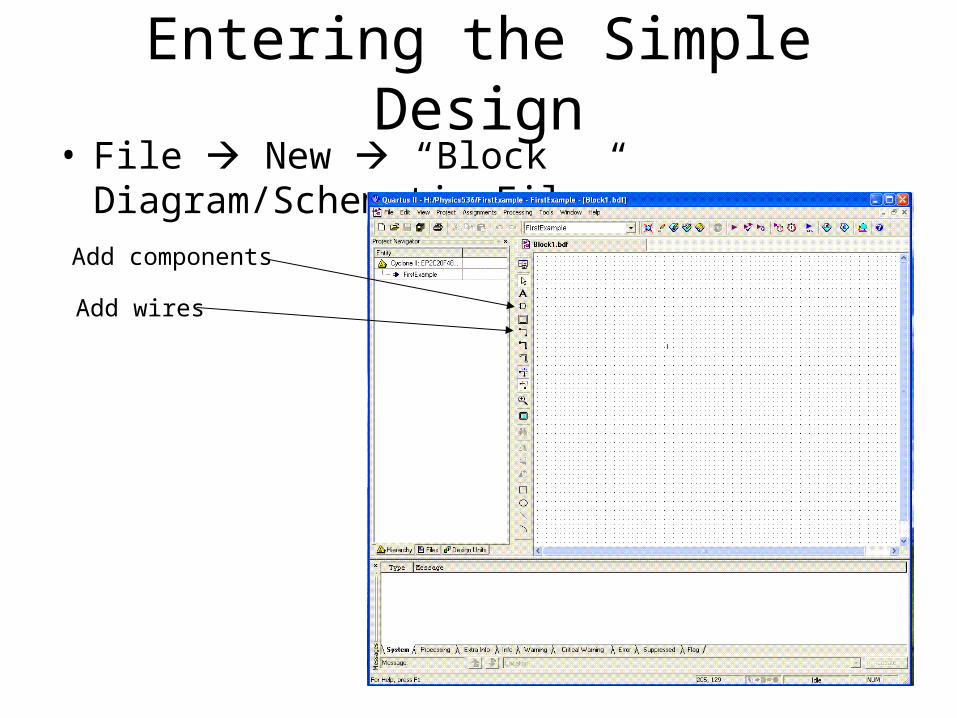
Entering the Simple Design• File New “Block Diagram/Schematic File”
Add components
Add wires
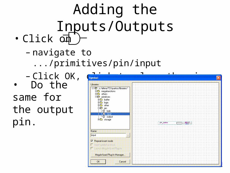
Adding the Inputs/Outputs• Click on
– navigate to .../primitives/pin/input– Click OK, click to place the pin.
• Do the same for the output pin.
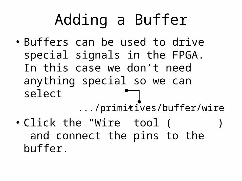
Adding a Buffer• Buffers can be used to drive special
signals in the FPGA. In this case we don’t need anything special so we can select .../primitives/buffer/wire
• Click the “Wire” tool ( ) and connect the pins to the buffer.
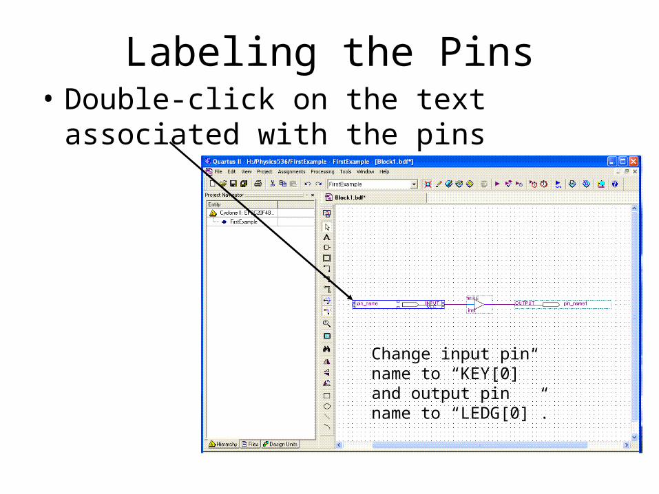
Labeling the Pins• Double-click on the text associated with
the pins
Change input pin name to “KEY[0]” and output pin name to “LEDG[0]”.
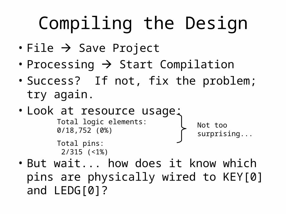
Compiling the Design• File Save Project
• Processing Start Compilation
• Success? If not, fix the problem; try again.
• Look at resource usage:
• But wait... how does it know which pins are physically wired to KEY[0] and LEDG[0]?
Total logic elements: 0/18,752 (0%)
Total pins: 2/315 (<1%)Not too surprising...
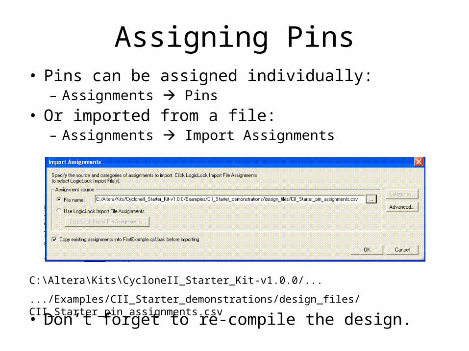
Assigning Pins• Pins can be assigned individually:
– Assignments Pins
• Or imported from a file:– Assignments Import Assignments
• Don’t forget to re-compile the design.
C:\Altera\Kits\CycloneII_Starter_Kit-v1.0.0/...
.../Examples/CII_Starter_demonstrations/design_files/CII_Starter_pin_assignments.csv
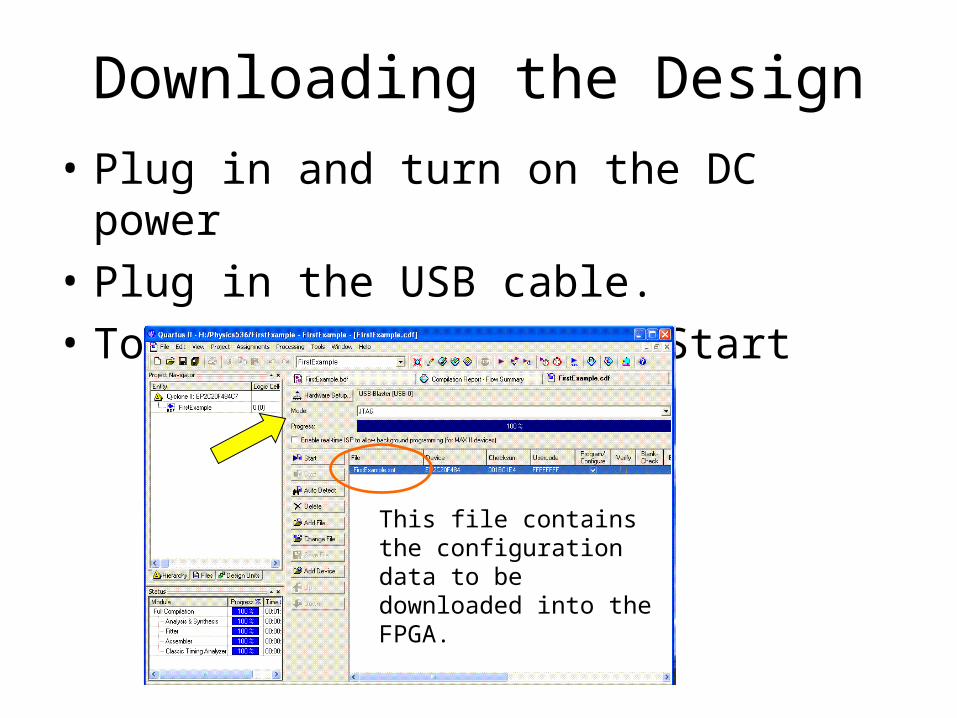
Downloading the Design
• Plug in and turn on the DC power
• Plug in the USB cable.
• Tools Programmer Start
This file contains the configuration data to be downloaded into the FPGA.
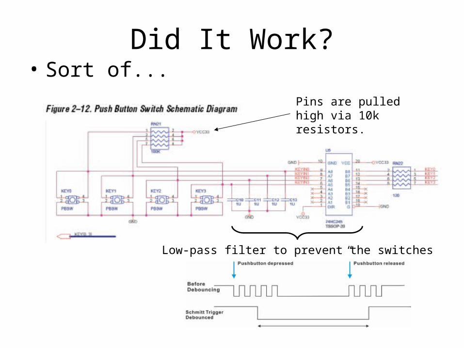
Did It Work?• Sort of...
Pins are pulled high via 10k resistors.
Low-pass filter to prevent the switches from “bouncing”.
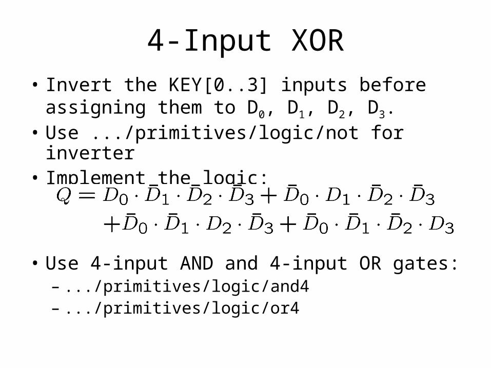
4-Input XOR
• Invert the KEY[0..3] inputs before assigning them to D0, D1, D2, D3.
• Use .../primitives/logic/not for inverter• Implement the logic:
• Use 4-input AND and 4-input OR gates:– .../primitives/logic/and4– .../primitives/logic/or4
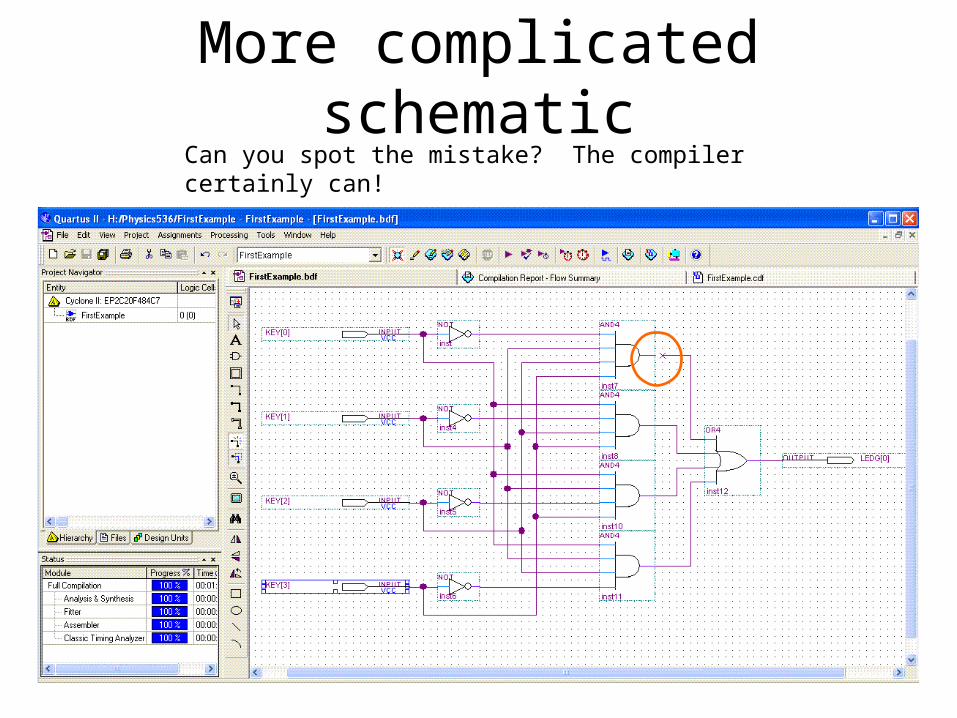
More complicated schematicCan you spot the mistake? The compiler certainly can!
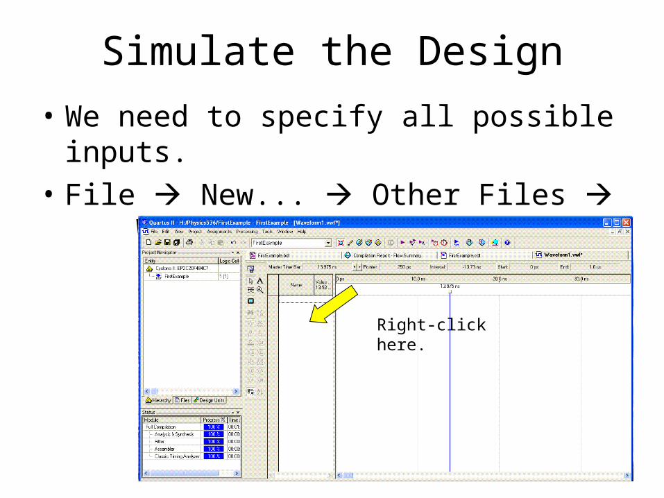
Simulate the Design
• We need to specify all possible inputs.
• File New... Other Files Waveform Vector File
Right-click here.
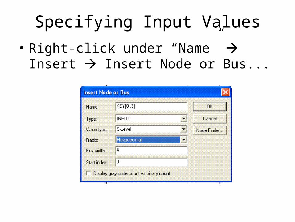
Specifying Input Values
• Right-click under “Name” Insert Insert Node or Bus...
Specifying Input Values
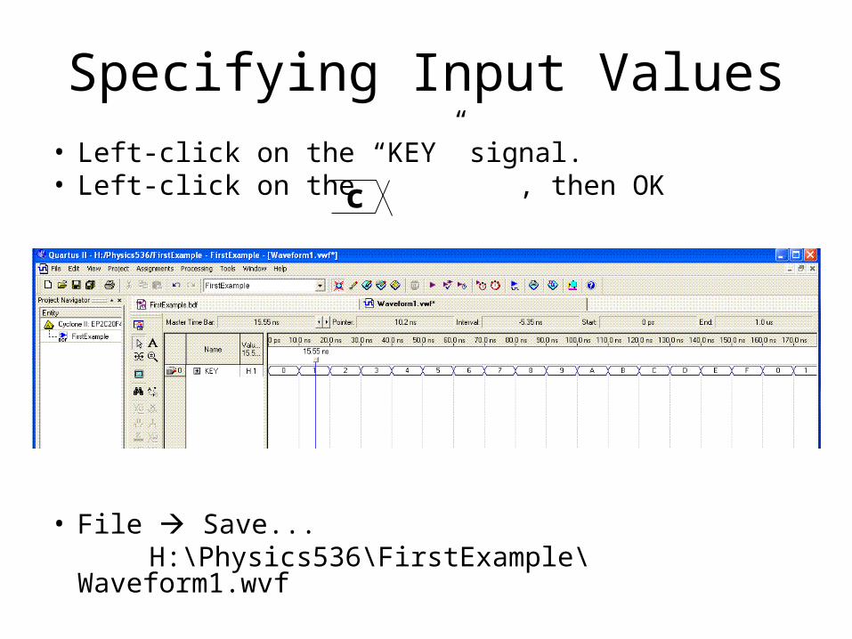
• Left-click on the “KEY” signal.• Left-click on the , then OK
• File Save... H:\Physics536\FirstExample\Waveform1.wvf
c
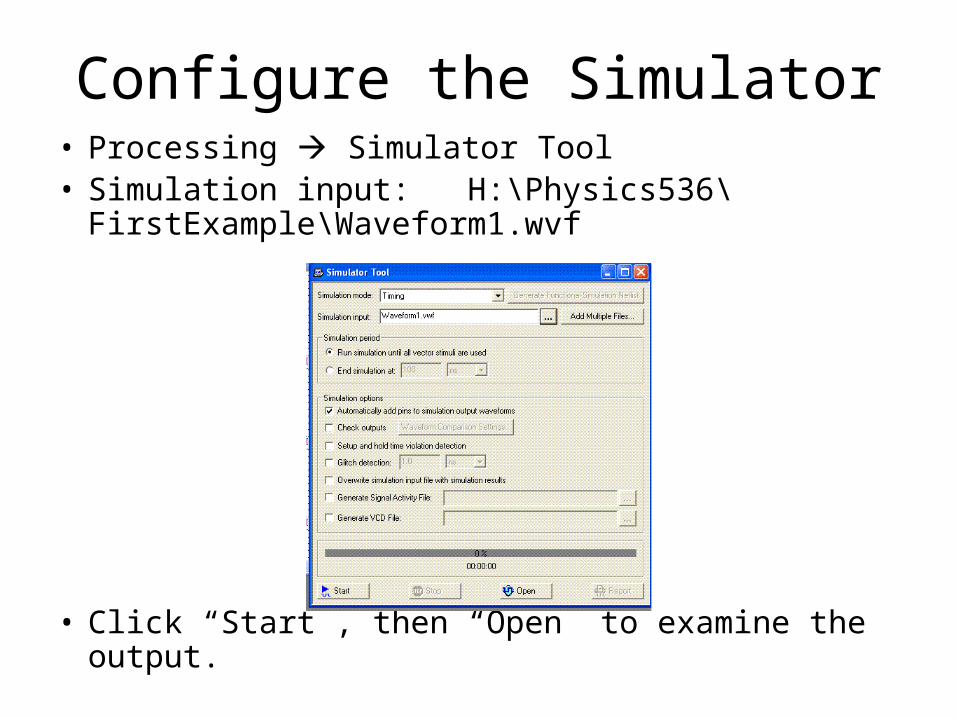
Configure the Simulator• Processing Simulator Tool• Simulation input: H:\Physics536\FirstExample\
Waveform1.wvf
• Click “Start”, then “Open” to examine the output.
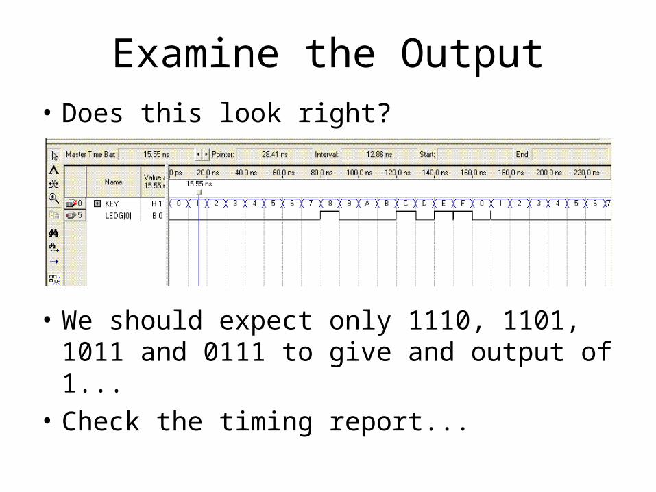
Examine the Output
• Does this look right?
• We should expect only 1110, 1101, 1011 and 0111 to give and output of 1...
• Check the timing report...
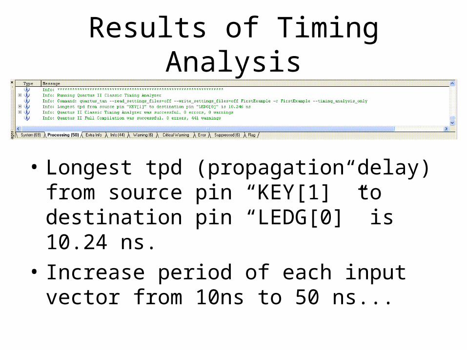
Results of Timing Analysis
• Longest tpd (propagation delay) from source pin “KEY[1]” to destination pin “LEDG[0]” is 10.24 ns.
• Increase period of each input vector from 10ns to 50 ns...
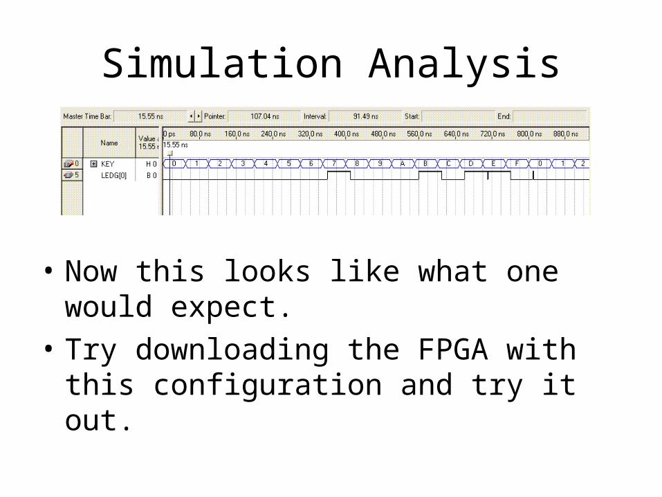
Simulation Analysis
• Now this looks like what one would expect.
• Try downloading the FPGA with this configuration and try it out.


![FPGA-Based Implementation of IEEE 802.16d WiMAX …... thus Implementation design ... has implemented an OFDM transmitter on Altera Statix II FPGA ... [17], Implemented OFDM transmitter](https://img.pdfslide.us/doc/110x75/5acf24d37f8b9a8b1e8c527c/fpga-based-implementation-of-ieee-80216d-wimax-thus-implementation-design.jpg)