Embed Size (px)
Citation preview

1
Introduction to Electronics
Section 1.3
1

2
Analog vs. Digital
• Analog Signal– Can take on any value– Most signals around us are like this
• Digital Signal– Sequence of numbers– Each number is an approximation of an analog
signal at an instant of time– Usually represented using binary number system

3
Figure 1.7 Sampling the continuous-time analog signal in (a) results in the discrete-time signal in (b).

4
Figure 1.8 Variation of a particular binary digital signal with time.

5
Figure 1.9 Block-diagram representation of the analog-to-digital converter (ADC).

6
Diodes
Sections 3.7.1
6

7
Semiconductor Materials
• silicon, germanium, gallium arsenide• conductivity => number of free charge carriers per
unit volume• metal --- high conductivity• insulator --- low conductivity• semiconductor --- variable conductivity changed by
the addition of dopants• crystalline structure with covalent bonds• at T = 0 insulator (i.e no free charge carriers)

8
Figure 3.39 Simplified physical structure of the junction diode. (Actual geometries are given in Appendix A.)

9
Figure 3.40 Two-dimensional representation of the silicon crystal. The circles represent the inner core of silicon atoms, with +4 indicating its positive charge of +4q, which is neutralized by the charge of the four valence electrons. Observe how the covalent bonds are formed by sharing of the valence electrons. At 0 K, all bonds are intact and no free electrons are available for current conduction.

10
Figure 3.41 At room temperature, some of the covalent bonds are broken by thermal ionization. Each broken bond gives rise to a free electron and a hole, both of which become available for current conduction.

11
• generated hole - electron pairs• electron --- negative• hole --- positive• holes and electrons can contribute to current• equal number of holes and electrons called
“intrinsic” semiconductor

12
Diffusion and Drift
• Diffusion– Random motion due to thermal agitation– Carriers move from high to low concentration– Results in diffusion current
• Drift– Movement of carriers due to electric field– Drift velocity depends on mobility of carrier and
magnitude of electric field– Results in drift current

13
Diffusion
Figure 3.42 A bar of intrinsic silicon (a) in which the hole concentration profile shown in (b) has been created along the x-axis by some unspecified mechanism.

14
• Drift– A hole migrates to the right as different electrons fill in the hole’s
vacancy by moving one site to the left. – The motion of the individual electrons is toward the left, against the
electric field, net hole motion is toward the right (i.e.: in the direction of the electric field).

15
Dopants
• hole/electron concentrations can be changed by the additions of small amounts of elements (dopants) to create “extrinsic” semiconductor
• Dopants– acceptors - boron, indium, aluminum – p type– donors - phosphorous, arsenic, antimony (have extra
electron) – n type• maintain charge neutrality• minimum amount of energy to move unbound
electrons/holes (i.e. easy to jump from one site to another)

16
Figure 3.43 A silicon crystal doped by a pentavalent element. Each dopant atom donates a free electron and is thus called a donor. The doped semiconductor becomes n type.
17
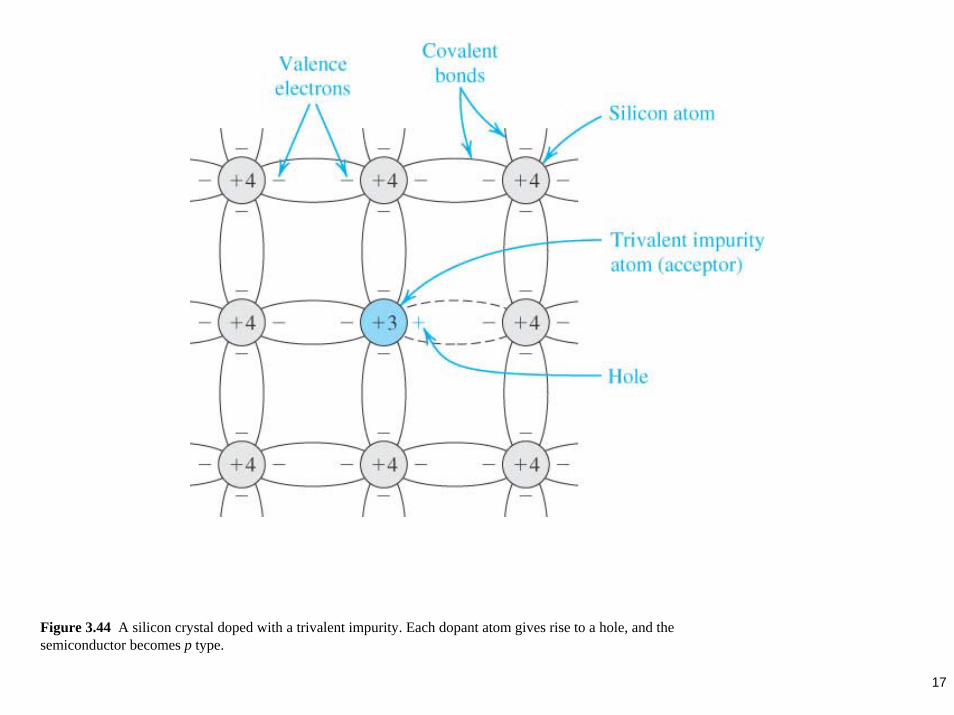
Figure 3.44 A silicon crystal doped with a trivalent impurity. Each dopant atom gives rise to a hole, and the semiconductor becomes p type.