Embed Size (px)
Citation preview
1
Introduction to Electrical Measurements
and Electronic Circuits.
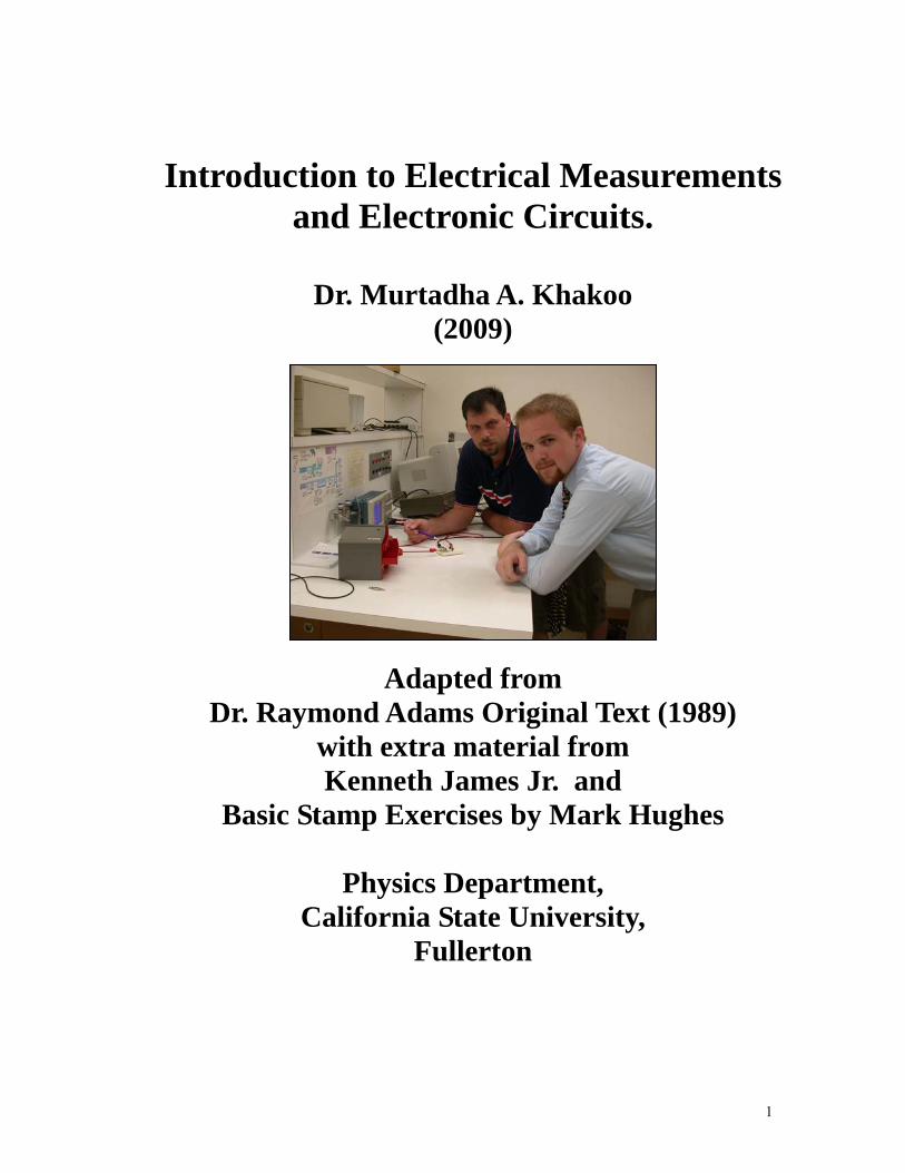
Dr. Murtadha A. Khakoo (2009)
Adapted from Dr. Raymond Adams Original Text (1989)
with extra material from Kenneth James Jr. and
Basic Stamp Exercises by Mark Hughes
Physics Department, California State University,
Fullerton
2
Aims of the Laboratory and Philosophy. The aims of this laboratory is also to make you able to keep a professional scientific laboratory record of what you did so that it can be reviewed (in this case by others) to see what was done. It is also a lab. that instructs on emergency Band-Aid electronics, which some of you will need in your future employment. You should also "collaborate"/"brain-storm" with your colleagues to enable you to go through the exercise. This will foster collaborative research spirit in your professional outlook. Remember you can always learn from exchanging ideas (both parties). Laboratory Note Book The recommended book is the 10X7.87, 5X5 Quad (approx $3) which has grilled rule. (National #53-110, or equivalent). IMP.: You should do all the formal exercise on the right page of the notebook leaving the other page for comments, calculations for yourself. Keeping this laboratory note book up to date is a very good strategy to succeed. Recommended Text The recommended texts are: The Art of Electronics (Paperback), by P.Horowitz and Hill, Cambridge Univ. Press, 1989-1992 or Introductory Electronics for Scientists and Engineeers Robert E. Simpson, Allyn and Bacon, Ed. 2, Addison-Wesley 1987. Both are very good reference books for our particular course. It is recommended that you browse through both references and use these whenever you can (often) to enable you to understand the basis of operation of the circuits. Other I do not approve of students dragging their heels and copying from others, and I expect you to put your honest effort to stay on schedule like most of the students in the class. Turning up late to class is going to be recorded in a register and will affect your grade. I will have the laboratory open by the Department Staff (upon request) on other hours, but you will not get any supervision during these hours. These laboratory hours are meant to enable you to catch up with the scheduled exercise, or to prepare for the coming exercise. Examination Prior to all the exams, there will be a pre-exam exercise i.e. you will be given an exercise to help you complete the test using the work you did to answer the pre-exam questions, else we will discuss pertinent example problems before the quiz. You will not be graded on the pre-quiz although this is crucial to your performance in the quiz (as expected).
3
Note to The Student This laboratory course, is developed as a practical course, with some emphasis on the underlying theory. However, much practical work in electronics can be done without a thorough understanding of the theory. Especially is this true when integrated circuits (IC's) are used. It normally is only necessary to understand how to connect and use the IC. Of course, a good knowledge of electronic measurement techniques is required. Do not be concerned when detailed theory of circuit operation is not fully covered in the laboratory course: this omission is intentional!
This laboratory manual is prepared for you to use in carrying out the experiments. Most of the theory involved is not in the manual. You are expected to read references (these are given on following pages for all experiments and are in the recommended texts) in order to learn the theory behind each experiment, and to obtain other valuable information concerning electronics. It will be necessary for your instructor to give you specific information concerning laboratory techniques, including how to operate the laboratory instrumentation. Prior to taking this course, most students have almost no practical knowledge of electronic instrumentation. It is the purpose of this course to provide you with the ability to use an oscilloscope, DC power supplies, function generators and multi-meters. [These are the most useful equipment items for use in electronics experimentation.] It is also the purpose of this course, after we review the basic concepts associated with circuit elements (resistors, capacitors, diodes and transistors), to introduce you to the wonderful world of integrated circuits. It is not possible, in the limited time of this course, to give you experience in more than a few of the many useful circuits that are based upon each integrated circuit. However, the introduction that you do get should make it possible for you to read about, and assemble and test, additional circuits as you need them. The present laboratory manual including the Basic Stamp™ Microprocessor exercises are also on Computer Disk and on your laboratory computer as an HTML file. A word concerning the excellent reference texts, Horowitz and Hill and Simpson: only a fraction of the pages of these texts are specifically referenced for these experiments. However, they are excellent references for your own physics library. Keep them and refer to them when you need a reference on some electronics circuit. Both texts’ indexes are an excellent starting point for locating the desired material. Browse through the text to get a perspective on what it contains. This text is currently used in the CSUF lecture course, Electronic Circuit Theory. That course, which is recommended to you, delves more deeply into the theory and practice of electronics for the physicist. Finally, enjoy learning the wonderful and powerful world of electronics and make sure you keep up with the course! Dr. Murtadha A. Khakoo, (2009)
4
SHORT TABLE OF CONTENTS
This is a short table of contents. For more detail, see the Assignment Schedule on the following
pages.
To find the pages for each experiment, look at lower right corner of pages for the experiment
number, look at the bottom center of the pages for the page number within the experiment
discussion. When Appendices are needed, they appear in pages that immediately follow the
individual experiment discussion.
EXPERIMENT ASSIGNMENT SCHEDULE
COMPONENTS LIST
EXP: 1 INSTRUMENT FAMILIARIZATION, DC CIRCUIT ANALYSIS
EXP: 2 RC CIRCUITS
EXP: 3 POWER DIODES, SIGNAL DIODES, ZENER DIODES
EXP: 4 TRANSISTORS
EXP: 5 OP-AMP CIRCUITS
EXP: 6 COMPARATOR IC CIRCUITS
EXP: 7 TIMER IC CIRCUITS
EXP: 8 PULSE SAMPLING CIRCUITS
EXP: 9 DIGITAL IC CIRCUITS: GATES, FLIP-FLOPS, ETC.
EXP: 10 BASIC STAMP EXERCISES
5
PHYSICS 380 LABORATORY - ASSIGNMENT SCHEDULE
This set of experiments is designed for 15 weeks of classes, with two 3-hour laboratory periods
each week. In addition, one hour of lecture each week is assumed.
Week Lab Day Assignment
1,2 1 EXP:1.1 INSTRUMENT FAMILIARIZATION: oscilloscope, function generator,
DC power supply, multimeter.
2 EXP:1.2 DC CIRCUIT ANALYSIS: series, parallel resistors, Thevenin & Norton
equivalent active circuits.
3 EXP:2.1 RC CIRCUITS: low-pass and high-pass RC filters, differentiators,
integrators, band-pass RLC circuit.
3 4 EXP:2.2 RC CIRCUITS: transient response, Laplace
transform method of circuit analysis
5 EXP:3.1 POWER DIODES: half-wave, full-wave bridge rectifier; IC voltage
regulator
4 6 EXP: 3.2 SIGNAL DIODES: clipper, clamp, frequency meter ZENER DIODES:
used as voltage regulators
7 EXP: 4.1 TRANSISTORS: PNP & NPN characteristic curves (using curve tracer)
EXP: 4.2 TRANSISTOR: switch circuit
5 8 EXP: 4.3 TRANSISTOR: emitter follower circuit
EXP: 4.4 TRANSISTOR: emitter-coupled amplifier
9 EXP: 4.5 TRANSISTOR: unity-gain phase splitter, unity-gain phase shifter
6 10 NO NEW EXPERIMENT - Wrap-up transistor experiments
11 STUDY: OP-AMP limitations: phase shift compensation, offset voltage, input
bias current, input offset voltage
Week Lab Day Assignment
7 12 EXP: 5.1 OP-AMP AMPLIFIERS: differential, non-inverting,
and inverting amplifiers
13 EXP: 5.2 OP-AMP ANALOG MATHEMATICS: integrator, differentiator and
summing amplifier,
8 14 EXP: 5.3 OP-AMP ACTIVE FILTERS: low-pass, high-pass and
band-pass filters
6
15 NO NEW EXPERLMENT - Wrap-up of OP-AMP experiments
9 16 EXP: 6.1 COMPARATOR IC: Schmidt trigger
EXP: 6.2 COMPARATOR IC: relaxation oscillator
17 EXP: 7.1 TIMER IC: monostable time delay
EXP: 7.2 TIMER IC: relaxation oscillator
10 18 EXP: 8.1 PULSE SAMPLING: peak voltage detector
EXP: 8.2 PULSE SAMPLING: sample-and-hold circuit
19 EXP: 9.1 DIGITAL IC GATES: NOT, AND, OR, NAND, NOR, FOR
Use of logic pulser
11 EXP: 9.2 DIGITAL ICs: logic circuits, Boolean algebra
21 EXP: 9.3 DIGITAL ICs: flip-flops constructed from NAND Gates
12 22 EXP: 9.4 DIGITAL ICs: counter (scaler) using JK flip-flops
23 EXP: 9.6 DIGITAL ICs: shift register, using TIC flip flops
13 24 EXP: 10.1 BASIC STAMP MICROPROCESSOR Ex. 1
25 EXP: 10.2 BASIC STAMP MICROPROCESSOR Ex. 2
14 26 EXP: 10.3 BASIC STAMP MICROPROCESSOR Ex. 3
27 EXP: 10.4 BASIC STAMP MICROPROCESSOR Ex. 4
28 EXP: 10.5 BASIC STAMP MICROPROCESSOR Ex. 5
15 COMPLETE YOUR LAB WRITE-UPS
7
COMPONENTS LIST
Resistors (*)1%, others 5% (6 each unless otherwise noted)
68 (2) 100 (2) 220 470 (2) lk(*4) 4.7k
5.6k (2) l0k(*4) 15k 22k 47k (2) 68k
82k (1) 100k(*4) 220k (4) 1M
Potentiometer 50k
Capacitors [uF = microfarad]
39 pF (2) 0.0033 uF (3) 0.01 uF (6)
0.1 uF (6) 100 uF (1) 4.7 uF tantalum (1)
Diodes
2N4002 silicon (4) 1N4728 3-V Zener (2); Light emitting, (LED, 3 Green and 3 Red)
Transistors
2N2222A (1) NPN general purpose silicon
2N2907A (1) PNP general purpose silicon (complementary to 2N2222A)
2N5245 (1) FET, N-channel silicon
Integrated Circuits (1 each, except as noted)
LM 301, LM 741 op-amps
353N dual op-amp - FET-input
LM 311 comparator; 556 (dual 555 timer)
7400 (2) quad NAND gate, not open collector
7450 dual 2-wide-AND-OR-INV gate (AND-NOR)
7473 (2) dual JK flip-flop with clear
74LS164 8-bit parallel output serial shift register
Miscellaneous items
VE48 (1) bridge rectifier
78L05 5-V voltage regulator
Note: Each station is has 1 dual-trace digital oscilloscope, 1 DC power supply (0 to +6V, 0 to
+18V, 0 to -18V), 1 function generator (0 to 100kHz.sine, square and triangle waveforms), 1
digital multimeter, 1 decade resistance box (0 to 10M). A 6.3VAC-output transformer with
center tap is provided for the diode-rectifier experiments.
8
GENERALLY USEFUL MATERIAL.
I. CIRCUIT BOARD WIRING INSTRUCTIONS:
Sample “Bread” Circuit Board Inter-Hole Connections. These will vary, but in general follow a
standard architecture. With reference to the drawing of the bread board below:
1. The uppermost holes marked X-X are wired together. Use for +Vcc (P/S voltage).
2. The lowermost holes marked Y-Y are wired together. Use for GROUND.
3. Each 5 holes in a single column marked A-B-C-D-E are wired together.
4. Each 5 holes in a single column marked F-G-H-I-J are wired together.
5. If you desire to have 10 holes in a single column (A-B-C-D-E-F-G-H-I-J) wired together,
you must place a jumper wire from E to F in the desired column.
6. Place IC chips with their pins in Rows E and F, and so that the IC's +Vcc pin is in the row
marked E. This will usually place the IC's power supply ground pin in the row marked F.
[Short jumper wires from Row A to X, and from Row J to Y can then be used for the power
supply connections.] If an IC such as the LM301 op-amp requires a -Vcc connection, the -Vcc
lead from the power supply must be connected to the board at a convenient column, ABCDE or
FGHIJ.
7. IMPORTANT: Good practice in preparing jumper wires is to strip them about 5-6mm and
make them about 1.5 times longer than their running length along the board. Do not connect
test leads to the legs of resistors, capacitors, transistor. You can make a bare wire U and put it
into the board in the same contact column or row as the device you want to connect to.
Neatness is exponential for getting correctly working circuits. Use pliers to work the leads into
the board neatly without twisting the wire. Avoid jumping wires over circuit components.
Plan View of a Small Typical Circuit Board
9
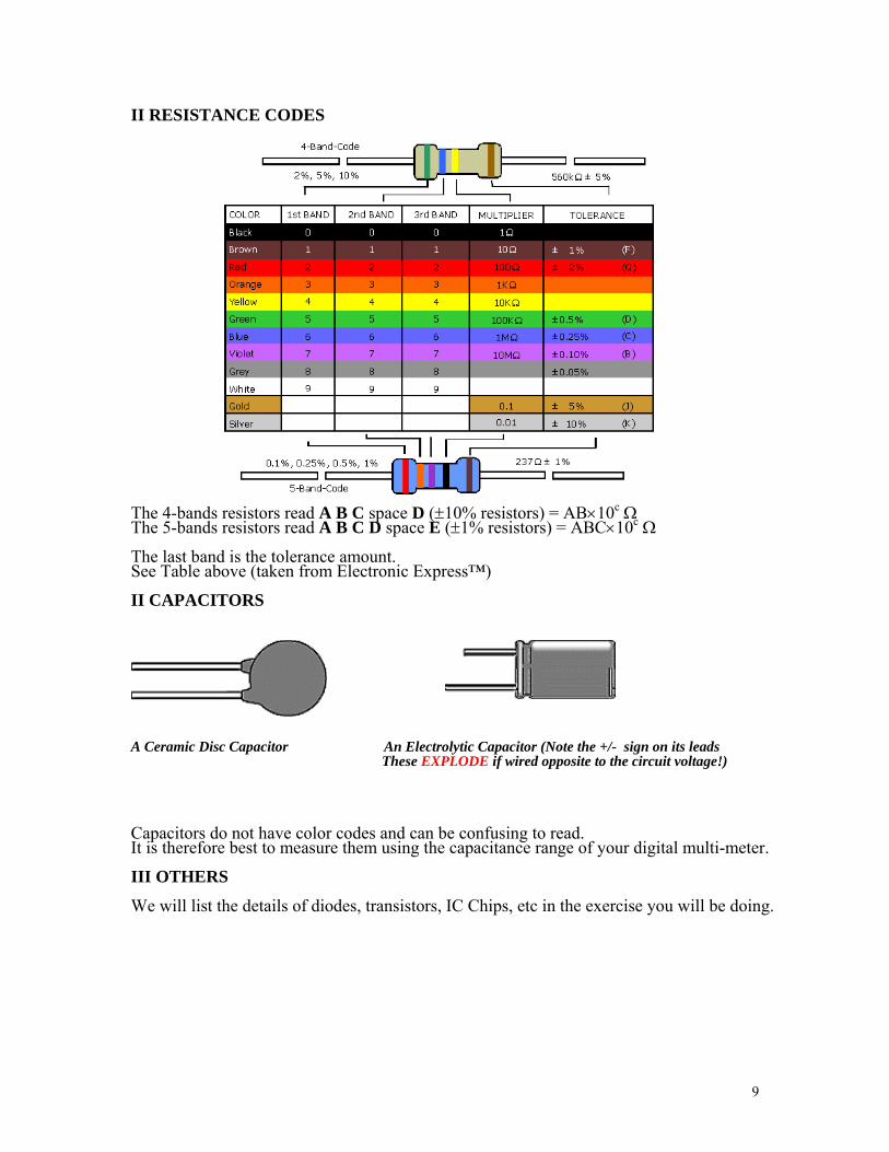
II RESISTANCE CODES
The 4-bands resistors read A B C space D (10% resistors) = AB10c The 5-bands resistors read A B C D space E (1% resistors) = ABC10c The last band is the tolerance amount. See Table above (taken from Electronic Express™) II CAPACITORS A Ceramic Disc Capacitor An Electrolytic Capacitor (Note the +/- sign on its leads These EXPLODE if wired opposite to the circuit voltage!) Capacitors do not have color codes and can be confusing to read. It is therefore best to measure them using the capacitance range of your digital multi-meter. III OTHERS We will list the details of diodes, transistors, IC Chips, etc in the exercise you will be doing.
10
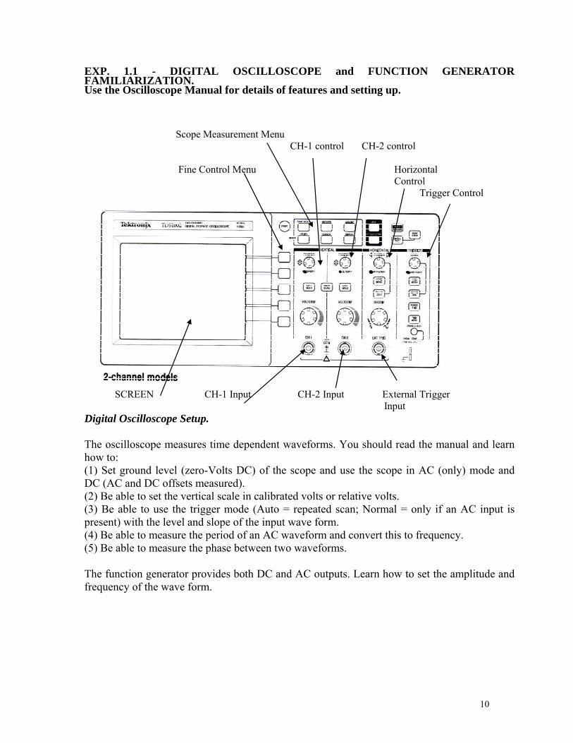
EXP. 1.1 - DIGITAL OSCILLOSCOPE and FUNCTION GENERATOR FAMILIARIZATION. Use the Oscilloscope Manual for details of features and setting up. Scope Measurement Menu CH-1 control CH-2 control Fine Control Menu Horizontal Control Trigger Control
SCREEN CH-1 Input CH-2 Input External Trigger Input
Digital Oscilloscope Setup. The oscilloscope measures time dependent waveforms. You should read the manual and learn how to: (1) Set ground level (zero-Volts DC) of the scope and use the scope in AC (only) mode and DC (AC and DC offsets measured). (2) Be able to set the vertical scale in calibrated volts or relative volts. (3) Be able to use the trigger mode (Auto = repeated scan; Normal = only if an AC input is present) with the level and slope of the input wave form. (4) Be able to measure the period of an AC waveform and convert this to frequency. (5) Be able to measure the phase between two waveforms. The function generator provides both DC and AC outputs. Learn how to set the amplitude and frequency of the wave form.
11
-3
-2
-1
0
1
2
3
0 1 2 3 4
t (ms)
V (
Vo
lts
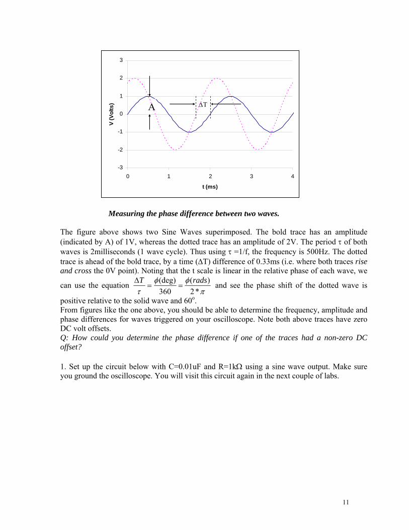
) A T
Measuring the phase difference between two waves. The figure above shows two Sine Waves superimposed. The bold trace has an amplitude (indicated by A) of 1V, whereas the dotted trace has an amplitude of 2V. The period of both waves is 2milliseconds (1 wave cycle). Thus using =1/f, the frequency is 500Hz. The dotted trace is ahead of the bold trace, by a time (T) difference of 0.33ms (i.e. where both traces rise and cross the 0V point). Noting that the t scale is linear in the relative phase of each wave, we
can use the equation
*2
)(
360
(deg) radsT
and see the phase shift of the dotted wave is
positive relative to the solid wave and 60o. From figures like the one above, you should be able to determine the frequency, amplitude and phase differences for waves triggered on your oscilloscope. Note both above traces have zero DC volt offsets. Q: How could you determine the phase difference if one of the traces had a non-zero DC offset? 1. Set up the circuit below with C=0.01uF and R=1k using a sine wave output. Make sure you ground the oscilloscope. You will visit this circuit again in the next couple of labs.
12
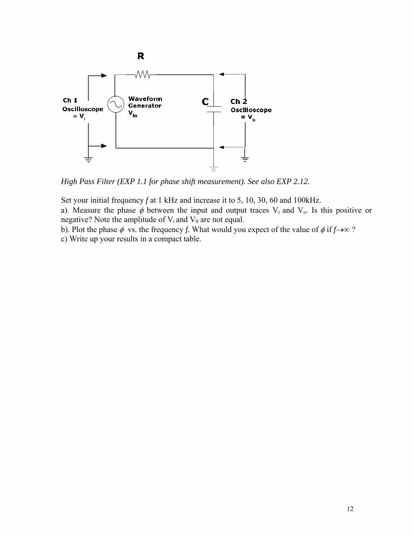
High Pass Filter (EXP 1.1 for phase shift measurement). See also EXP 2.12. Set your initial frequency f at 1 kHz and increase it to 5, 10, 30, 60 and 100kHz. a). Measure the phase between the input and output traces Vi and Vo. Is this positive or negative? Note the amplitude of Vi and V0 are not equal. b). Plot the phase vs. the frequency f. What would you expect of the value of if f?c) Write up your results in a compact table.
13
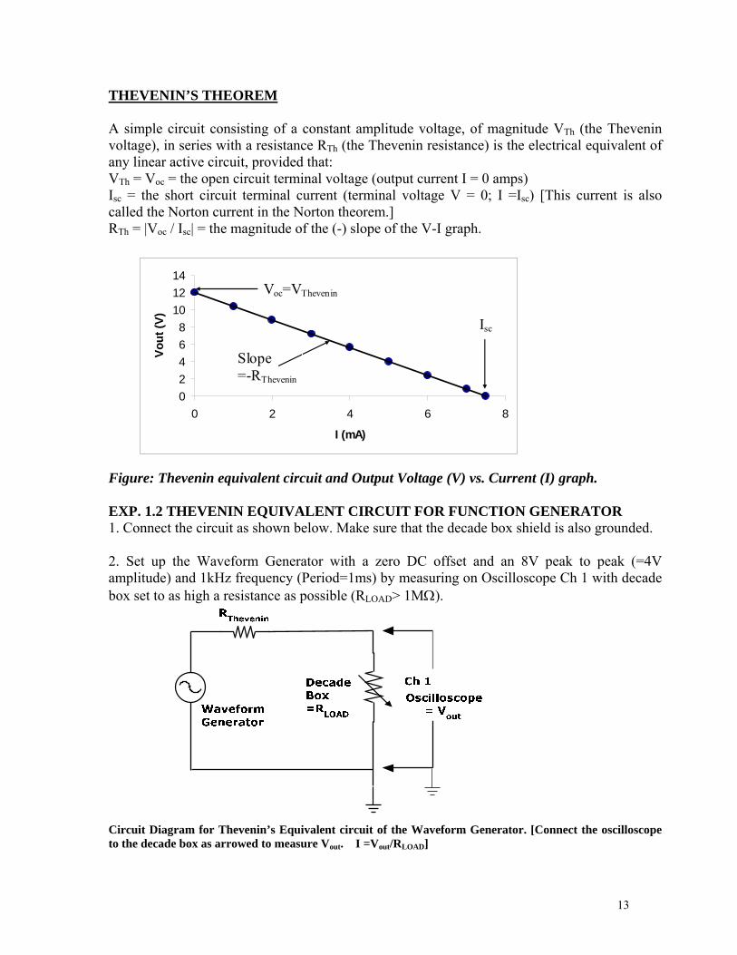
THEVENIN’S THEOREM A simple circuit consisting of a constant amplitude voltage, of magnitude VTh (the Thevenin voltage), in series with a resistance RTh (the Thevenin resistance) is the electrical equivalent of any linear active circuit, provided that: VTh = Voc = the open circuit terminal voltage (output current I = 0 amps) Isc = the short circuit terminal current (terminal voltage V = 0; I =Isc) [This current is also called the Norton current in the Norton theorem.] RTh = |Voc / Isc| = the magnitude of the (-) slope of the V-I graph.
0
2
4
6
8
10
12
14
0 2 4 6 8
I (mA)
Vo
ut
(V)
Voc=VThevenin
Isc
Slope =-RThevenin
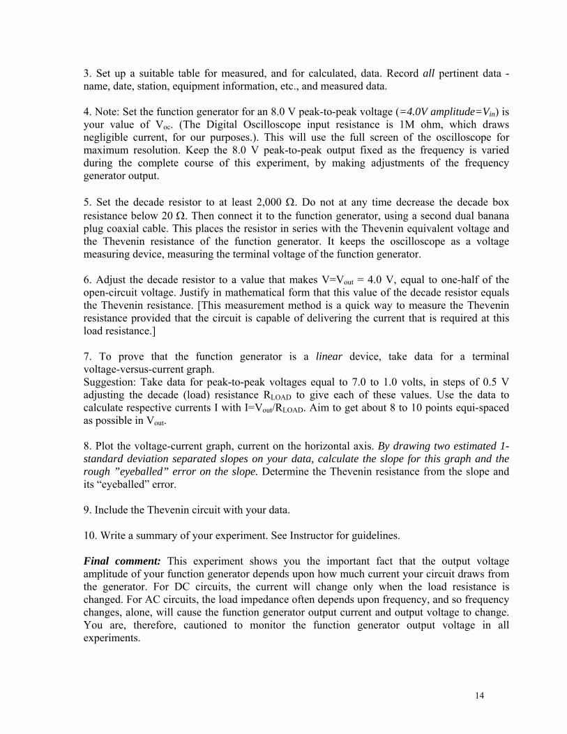
Figure: Thevenin equivalent circuit and Output Voltage (V) vs. Current (I) graph. EXP. 1.2 THEVENIN EQUIVALENT CIRCUIT FOR FUNCTION GENERATOR 1. Connect the circuit as shown below. Make sure that the decade box shield is also grounded. 2. Set up the Waveform Generator with a zero DC offset and an 8V peak to peak (=4V amplitude) and 1kHz frequency (Period=1ms) by measuring on Oscilloscope Ch 1 with decade box set to as high a resistance as possible (RLOAD> 1M).
Circuit Diagram for Thevenin’s Equivalent circuit of the Waveform Generator. [Connect the oscilloscope to the decade box as arrowed to measure Vout. I =Vout/RLOAD]
14
3. Set up a suitable table for measured, and for calculated, data. Record all pertinent data - name, date, station, equipment information, etc., and measured data. 4. Note: Set the function generator for an 8.0 V peak-to-peak voltage (=4.0V amplitude=Vin) is your value of Voc. (The Digital Oscilloscope input resistance is 1M ohm, which draws negligible current, for our purposes.). This will use the full screen of the oscilloscope for maximum resolution. Keep the 8.0 V peak-to-peak output fixed as the frequency is varied during the complete course of this experiment, by making adjustments of the frequency generator output. 5. Set the decade resistor to at least 2,000 . Do not at any time decrease the decade box resistance below 20 . Then connect it to the function generator, using a second dual banana plug coaxial cable. This places the resistor in series with the Thevenin equivalent voltage and the Thevenin resistance of the function generator. It keeps the oscilloscope as a voltage measuring device, measuring the terminal voltage of the function generator. 6. Adjust the decade resistor to a value that makes V=Vout = 4.0 V, equal to one-half of the open-circuit voltage. Justify in mathematical form that this value of the decade resistor equals the Thevenin resistance. [This measurement method is a quick way to measure the Thevenin resistance provided that the circuit is capable of delivering the current that is required at this load resistance.] 7. To prove that the function generator is a linear device, take data for a terminal voltage-versus-current graph. Suggestion: Take data for peak-to-peak voltages equal to 7.0 to 1.0 volts, in steps of 0.5 V adjusting the decade (load) resistance RLOAD to give each of these values. Use the data to calculate respective currents I with I=Vout/RLOAD. Aim to get about 8 to 10 points equi-spaced as possible in Vout. 8. Plot the voltage-current graph, current on the horizontal axis. By drawing two estimated 1-standard deviation separated slopes on your data, calculate the slope for this graph and the rough ”eyeballed” error on the slope. Determine the Thevenin resistance from the slope and its “eyeballed” error. 9. Include the Thevenin circuit with your data. 10. Write a summary of your experiment. See Instructor for guidelines. Final comment: This experiment shows you the important fact that the output voltage amplitude of your function generator depends upon how much current your circuit draws from the generator. For DC circuits, the current will change only when the load resistance is changed. For AC circuits, the load impedance often depends upon frequency, and so frequency changes, alone, will cause the function generator output current and output voltage to change. You are, therefore, cautioned to monitor the function generator output voltage in all experiments.
15
QUESTION: How do I write up my Lab. Report?
A SUGGESTED FORMAT FOR YOUR LABORATORY WRITE-UP:
8.1 Aim. State the aim of the experiment in brief and clear terms. Do not get personal. Stay
objective.
8.2 Setup/Apparatus. Describe the equipment used; a diagram, carefully/clearly labeled, easily
read and not crunched-up diagram is worth a thousand words.
8.3 Method. Describe very briefly what you did. Pay attention to things you worked out additional
to the laboratory handbook.
8.4 Measurements/Observations/Analysis. Discuss the data acquired and tabulate/plot them. Use
your unbounded investigative spirit and creativity. Label clearly your figures and graphs (do
not miss out the x and y coordinates’ variables and dimensions).
8.5 Conclusions. Discuss your conclusions. This should be the most creative part of the whole
exercise. It should elaborate on the overall discussions of your results from an objective
viewpoint, errors and points of argument concerning validity of hypotheses you made, in the
earlier sections of this write-up. Discussions of errors and improvement of experiments go
here. Be creative! This is the part that demonstrates to the reader how much you understood
about the laboratory exercise. It will the part I will judge you the most.
Remember to be objective and not personal and subjective. You should not write superfluous
statements as “I really liked this experiment” or “This was an experiment I hated” or “I was not
feeling very well during this experiment”. You can say things like “This experiment could be
greatly improved by ..” and then elaborate on your creative ideas to do the improvement.
Observations that look interesting (even better if accompanied with explanations) should be
included. Or “We observed this and it could be explained by this, giving a possible explanation
of your observation during the course of your experimental exercise. Impress the reader!
8.6 Finally, try to be as neat as you possibly can. If you make a mistake, just draw a line through
the mistake. Do not try to erase it. Your lab write-up should be mainly in ink and not pencil
(except for the graphs, drawings, etc).
16
EXP 2. RC CIRCUITS
Introduction EXP. 2.1 deals with RC circuits that are driven by periodic waveforms: sine waveforms for the filter circuits, and sine, square and triangle waveforms for the integrator and differentiator circuits. EXP. 2.2 deals with RC circuits when they are subject to sudden changes in input voltages, resulting in transient effects that die out rapidly with time. Discussion of EXP. 2.1 experiments Linear analog circuits are often driven by sinusoidal voltages or by other periodic voltages (which by the Fourier series theorem are a linear summation of sinusoidal voltages of many different harmonic frequencies). In such circuits, either by design or by necessity, RC filters are used to eliminate (or enhance) input voltages of selected frequencies. Principal types of filters are: 1. High pass filters: those that pass all frequencies higher than a crossover frequency, which is also, called the cut-off frequency. 2. Low pass filters: those that pass all frequencies lower than a crossover frequency. 3. Band pass filters: those that pass a range of frequencies between a lower cut-off frequency and a higher cut-off frequency. The pass band may be quite wide, or quite narrow. [We also have notch filters that pass all frequencies except for a narrow band of frequencies.] 4. Filter Properties: There are two properties of filters that are of particular importance in electronic circuits: 1. The attenuation of the filter as a function of frequency, usually expressed in decibels (dB). A passive filter usually (but not always) has the attenuation: Amplitude: dB=20 log |Vo/Vi| and Power: dB=10 log |Po/Pi| and equal to 0dB in the center of the pass band (i.e. no attenuation). A 3dB roll off in amplitude is an amplitude attenuation of 1/ 2=0.7071, and a 3dB roll off in power is a power attenuation of (1/ 2)2=0.5. Here “o” and “i” subscripts appertain to the output and input. Outside the pass band the attenuation rapidly increases for frequencies beyond the crossover frequency. 2. The phase shift of the output voltage, with reference to the phase of the input voltage, as a function of frequency. This property's importance will appear later when we discuss feedback circuits. However, you have already visited this in Expt. 1.1. In all our filter experiments, we shall measure both attenuation and phase shift.
17
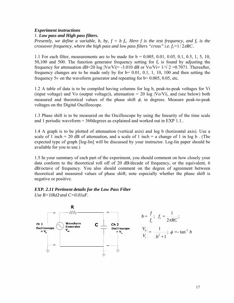
Experiment instructions 1. Low pass and High pass filters. Presently, we define a variable, b, by, f = b fc. Here f is the test frequency, and fc is the crossover frequency, where the high pass and low pass filters “cross” i.e. fc=1 2/ RC . 1.1 For each filter, measurements are to be made for b = 0.005, 0.01, 0.05, 0.1, 0.5, 1, 5, 10, 50,100 and 500. The function generator frequency setting for fc is found by adjusting the frequency for attenuation dB=20 log |Vo/Vi|= -3.010 dB or Vo/Vi= 1/√ 2 =0.7071. Thereafter, frequency changes are to be made only by for b= 0.01, 0.1, 1, 10, 100 and then setting the frequency 5 on the waveform generator and repeating for b= 0.005, 0.05, etc. 1.2 A table of data is to be compiled having columns for log b, peak-to-peak voltages for Vi (input voltage) and Vo (output voltage)), attenuation = 20 log |Vo/Vi|, and (see below) both measured and theoretical values of the phase shift , in degrees. Measure peak-to-peak voltages on the Digital Oscilloscope. 1.3 Phase shift is to be measured on the Oscilloscope by using the linearity of the time scale and 1 periodic waveform = 360degrees as explained and worked out in EXP 1.1.. 1.4 A graph is to be plotted of attenuation (vertical axis) and log b (horizontal axis). Use a scale of 1 inch = 20 dB of attenuation, and a scale of 1 inch = a change of 1 in log b . (The expected type of graph [log-lin] will be discussed by your instructor. Log-lin paper should be available for you to use.) 1.5 In your summary of each part of the experiment, you should comment on how closely your data conform to the theoretical roll off of 20 dB/decade of frequency, or the equivalent, 6 dB/octave of frequency. You also should comment on the degree of agreement between theoretical and measured values of phase shift; note especially whether the phase shift is negative or positive. EXP. 2.11 Pertinent details for the Low Pass Filter Use R=10k and C=0.01uF.
bf
ff
RC
V
V b
c
c
i
; ;
; - tan-1 b
1
2
1
1
0
2
18
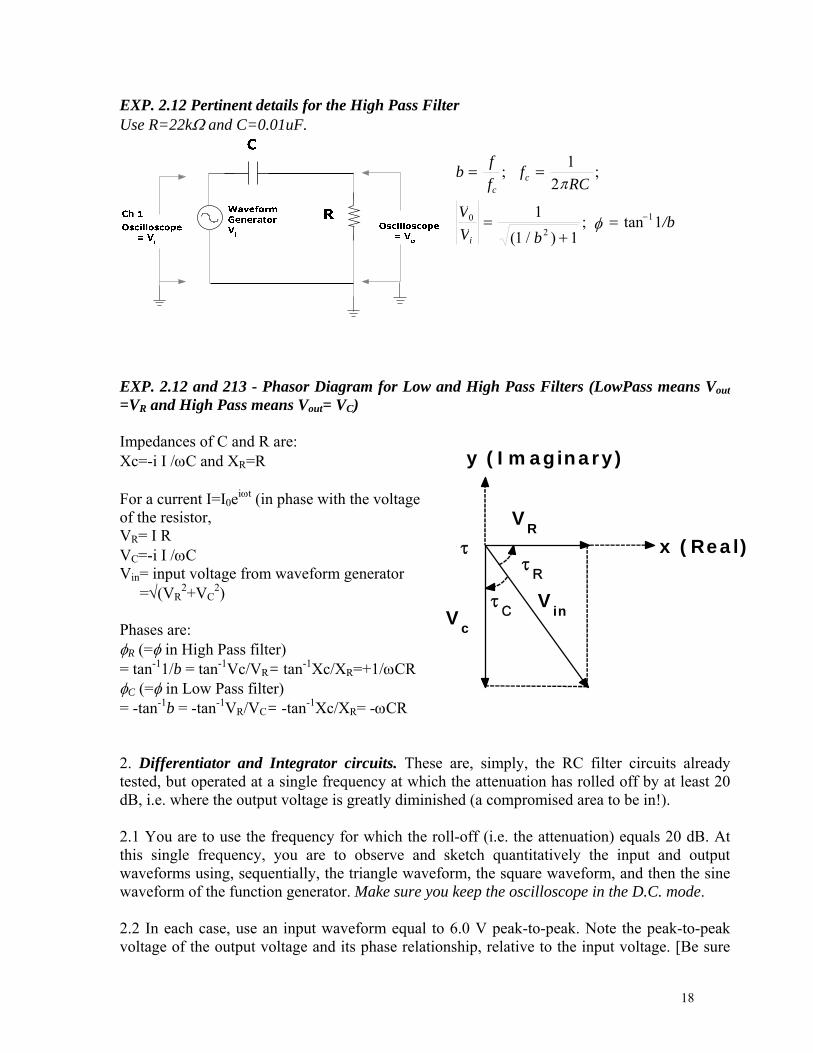
EXP. 2.12 Pertinent details for the High Pass Filter Use R=22k and C=0.01uF.
EXP. 2.12 and 213 - Phasor Diagram for Low and High Pass Filters (LowPass means Vout =VR and High Pass means Vout= VC) Impedances of C and R are: Xc=-i I /C and XR=R For a current I=I0e
it (in phase with the voltage of the resistor, VR= I R VC=-i I /C Vin= input voltage from waveform generator =(VR
2+VC2)
Phases are: R (=in High Pass filter) = tan-11/b = tan-1Vc/VR= tan-1Xc/XR=+1/CR C (=in Low Pass filter) = -tan-1b = -tan-1VR/VC= -tan-1Xc/XR= -CR 2. Differentiator and Integrator circuits. These are, simply, the RC filter circuits already tested, but operated at a single frequency at which the attenuation has rolled off by at least 20 dB, i.e. where the output voltage is greatly diminished (a compromised area to be in!). 2.1 You are to use the frequency for which the roll-off (i.e. the attenuation) equals 20 dB. At this single frequency, you are to observe and sketch quantitatively the input and output waveforms using, sequentially, the triangle waveform, the square waveform, and then the sine waveform of the function generator. Make sure you keep the oscilloscope in the D.C. mode. 2.2 In each case, use an input waveform equal to 6.0 V peak-to-peak. Note the peak-to-peak voltage of the output voltage and its phase relationship, relative to the input voltage. [Be sure
bf
ff
RC
V
V b
cc
i
; ;
( / ); tan 1/b
1
2
1
1 1 0
2
1
x (Real)
y (Imaginary)
VinV
c
VR
R
C
19
to use EXT TRIGGER mode with the input voltage as trigger source.] 2.3 Determine in each case what the output waveform should be (in waveform, amplitude and phase), by taking the derivative or the integral (as the case may be) of the input voltage and substituting it into the appropriate theoretical equation. 2.4 In your summary for each circuit, comment on the agreement, or lack of agreement, of experiment with theory. EXP. 2.13. Low Pass Filter as an Integrator (when b>10)
dtVRC
VRC
ff
fb ic
c
1ly consequent;
2
1; 0
(see EXP 2.11)
EXP. 2.14. High Pass Filter as a Differentiator. (when b<0.1)
dt
dVRCV
RCf
f
fb i
cc
0ly consequent;2
1;
(see EXP 2.12)
3. Band pass filter. Only if you have time, make frequency and phase shift measurements for the given band pass filter. This one is, simply, a high pass RC filter of lower cross-over frequency, followed by a low pass RC filter of higher cross-over frequency. This results in a band pass filter with cut-off frequencies that are, approximately, equal to the individual cutoff frequencies. ("Approximately" is used because the behavior of the first filter is modified by the loading on it produced by the second filter.) NOTE: This kind of band pass filter is not used when precise band width is desired, due to the lack of precision of common resistors and capacitors. When a very narrow band pass filter, centered on a precise frequency is desired (as is the case in radio and television receivers), circuits utilizing the resonance properties of inductance-capacitance circuits are used. 3.1 Unlike the previous filter circuit measurements, here you should make measurements in the range of attenuation between values of about -30 dB at each edge of the pass band, with about 3 measurements per decade at evenly spaced (log f) values, instead of only one measurement per decade, as before. 3.2 A limited number of phase shift measurements should be made; i.e., not made at every frequency for which attenuation is measured. A total of about 6-7 points should suffice. 3.3 Note that the attenuation, even at the center of the pass band, is less than 0 dB, i.e. you still attenuate at the center of the band pass.
20
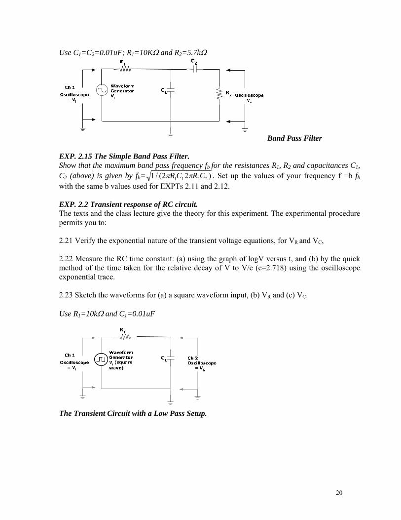
Use C1=C2=0.01uF; R1=10K and R2=5.7k
Band Pass Filter EXP. 2.15 The Simple Band Pass Filter. Show that the maximum band pass frequency fb for the resistances R1, R2 and capacitances C1, C2 (above) is given by fb= 1 2 21 1 2 2/ ( ) R C R C . Set up the values of your frequency f =b fb with the same b values used for EXPTs 2.11 and 2.12. EXP. 2.2 Transient response of RC circuit. The texts and the class lecture give the theory for this experiment. The experimental procedure permits you to: 2.21 Verify the exponential nature of the transient voltage equations, for VR and VC, 2.22 Measure the RC time constant: (a) using the graph of logV versus t, and (b) by the quick method of the time taken for the relative decay of V to V/e (e=2.718) using the oscilloscope exponential trace. 2.23 Sketch the waveforms for (a) a square waveform input, (b) VR and (c) VC. Use R1=10k and C1=0.01uF
The Transient Circuit with a Low Pass Setup.
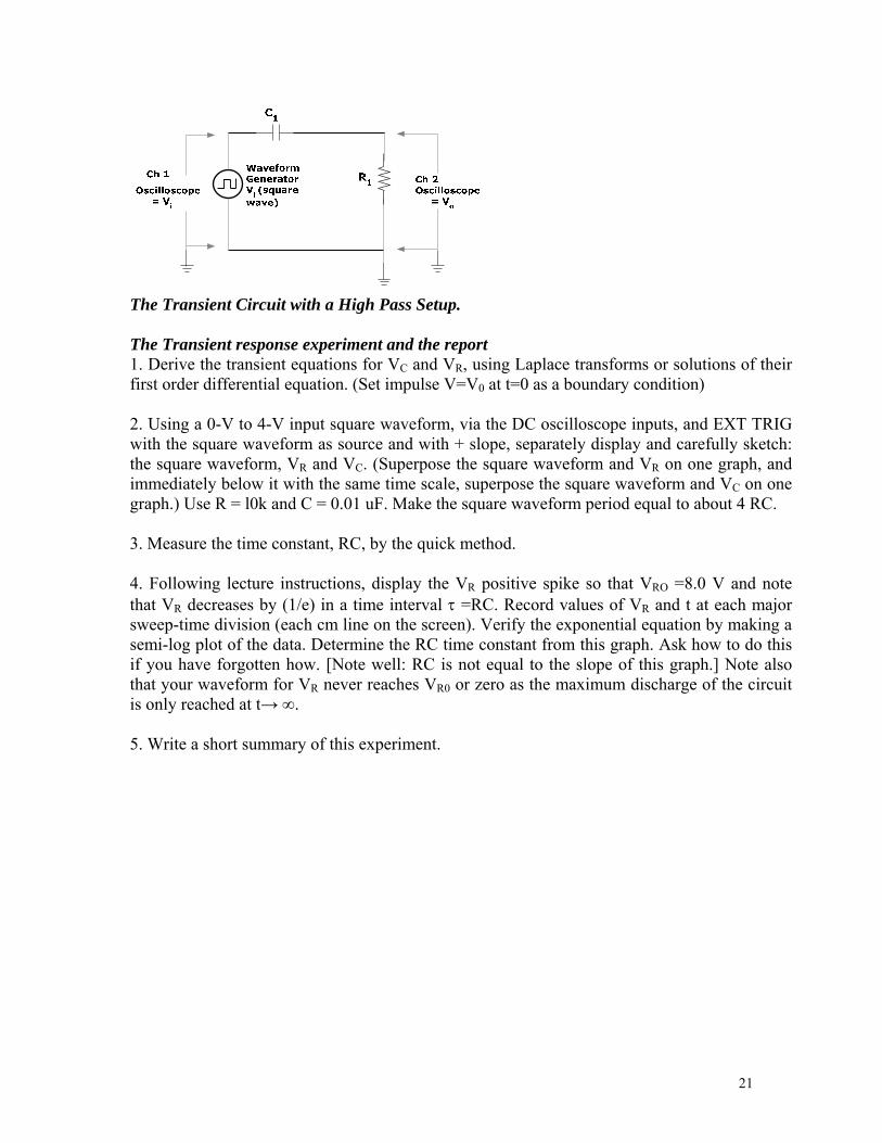
21
The Transient Circuit with a High Pass Setup. The Transient response experiment and the report 1. Derive the transient equations for VC and VR, using Laplace transforms or solutions of their first order differential equation. (Set impulse V=V0 at t=0 as a boundary condition) 2. Using a 0-V to 4-V input square waveform, via the DC oscilloscope inputs, and EXT TRIG with the square waveform as source and with + slope, separately display and carefully sketch: the square waveform, VR and VC. (Superpose the square waveform and VR on one graph, and immediately below it with the same time scale, superpose the square waveform and VC on one graph.) Use R = l0k and C = 0.01 uF. Make the square waveform period equal to about 4 RC. 3. Measure the time constant, RC, by the quick method. 4. Following lecture instructions, display the VR positive spike so that VRO =8.0 V and note that VR decreases by (1/e) in a time interval =RC. Record values of VR and t at each major sweep-time division (each cm line on the screen). Verify the exponential equation by making a semi-log plot of the data. Determine the RC time constant from this graph. Ask how to do this if you have forgotten how. [Note well: RC is not equal to the slope of this graph.] Note also that your waveform for VR never reaches VR0 or zero as the maximum discharge of the circuit is only reached at t→ ∞. 5. Write a short summary of this experiment.
22
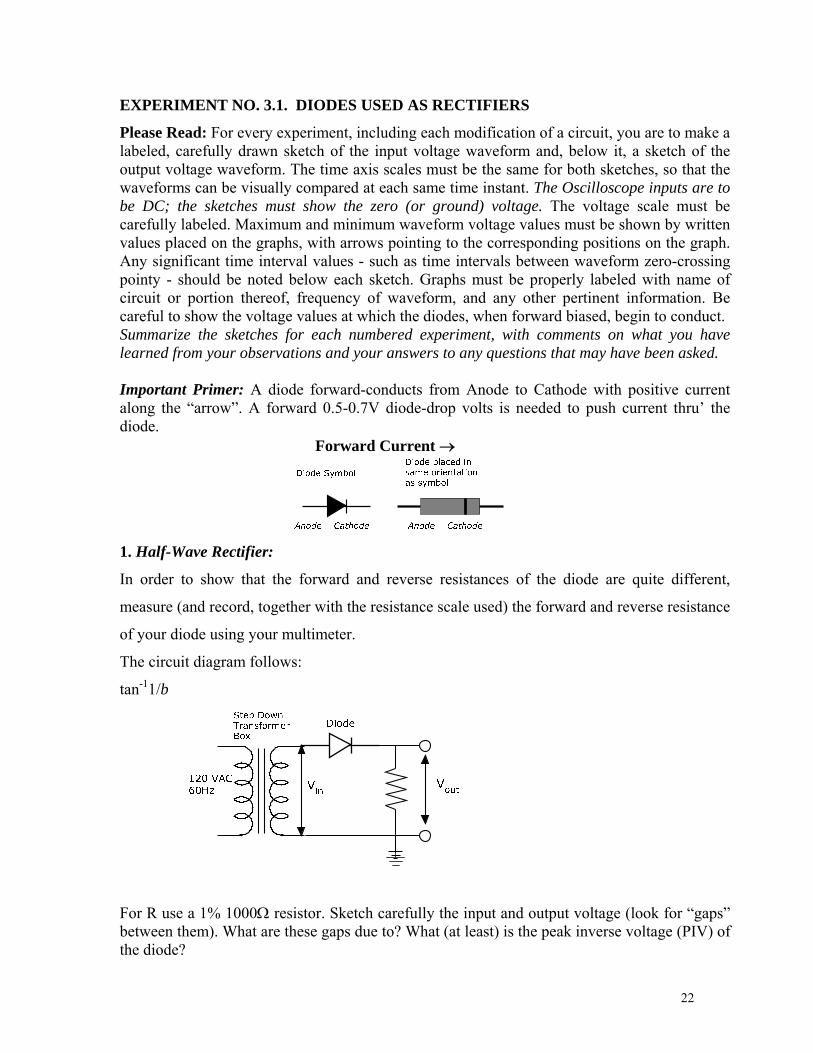
EXPERIMENT NO. 3.1. DIODES USED AS RECTIFIERS
Please Read: For every experiment, including each modification of a circuit, you are to make a labeled, carefully drawn sketch of the input voltage waveform and, below it, a sketch of the output voltage waveform. The time axis scales must be the same for both sketches, so that the waveforms can be visually compared at each same time instant. The Oscilloscope inputs are to be DC; the sketches must show the zero (or ground) voltage. The voltage scale must be carefully labeled. Maximum and minimum waveform voltage values must be shown by written values placed on the graphs, with arrows pointing to the corresponding positions on the graph. Any significant time interval values - such as time intervals between waveform zero-crossing pointy - should be noted below each sketch. Graphs must be properly labeled with name of circuit or portion thereof, frequency of waveform, and any other pertinent information. Be careful to show the voltage values at which the diodes, when forward biased, begin to conduct. Summarize the sketches for each numbered experiment, with comments on what you have learned from your observations and your answers to any questions that may have been asked. Important Primer: A diode forward-conducts from Anode to Cathode with positive current along the “arrow”. A forward 0.5-0.7V diode-drop volts is needed to push current thru’ the diode. Forward Current
1. Half-Wave Rectifier:
In order to show that the forward and reverse resistances of the diode are quite different,
measure (and record, together with the resistance scale used) the forward and reverse resistance
of your diode using your multimeter.
The circuit diagram follows:
tan-11/b
For R use a 1% 1000 resistor. Sketch carefully the input and output voltage (look for “gaps” between them). What are these gaps due to? What (at least) is the peak inverse voltage (PIV) of the diode?
23
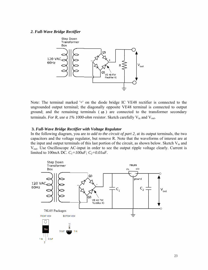
2. Full-Wave Bridge Rectifier
Note: The terminal marked '+' on the diode bridge IC VE48 rectifier is connected to the ungrounded output terminal; the diagonally opposite VE48 terminal is connected to output ground; and the remaining terminals ( ) are connected to the transformer secondary terminals. For R, use a 1% 1000-ohm resistor. Sketch carefully Vin and Vout.
3. Full-Wave Bridge Rectifier with Voltage Regulator In the following diagram, you are to add to the circuit of part 2, at its output terminals, the two capacitors and the voltage regulator, but remove R. Note that the waveforms of interest are at the input and output terminals of this last portion of the circuit, as shown below. Sketch Vin and Vout. Use Oscilloscope AC-input in order to see the output ripple voltage clearly. Current is limited to 100mA DC. C1=100uF; C2=0.01uF.
78L05
78L05 Packages
24
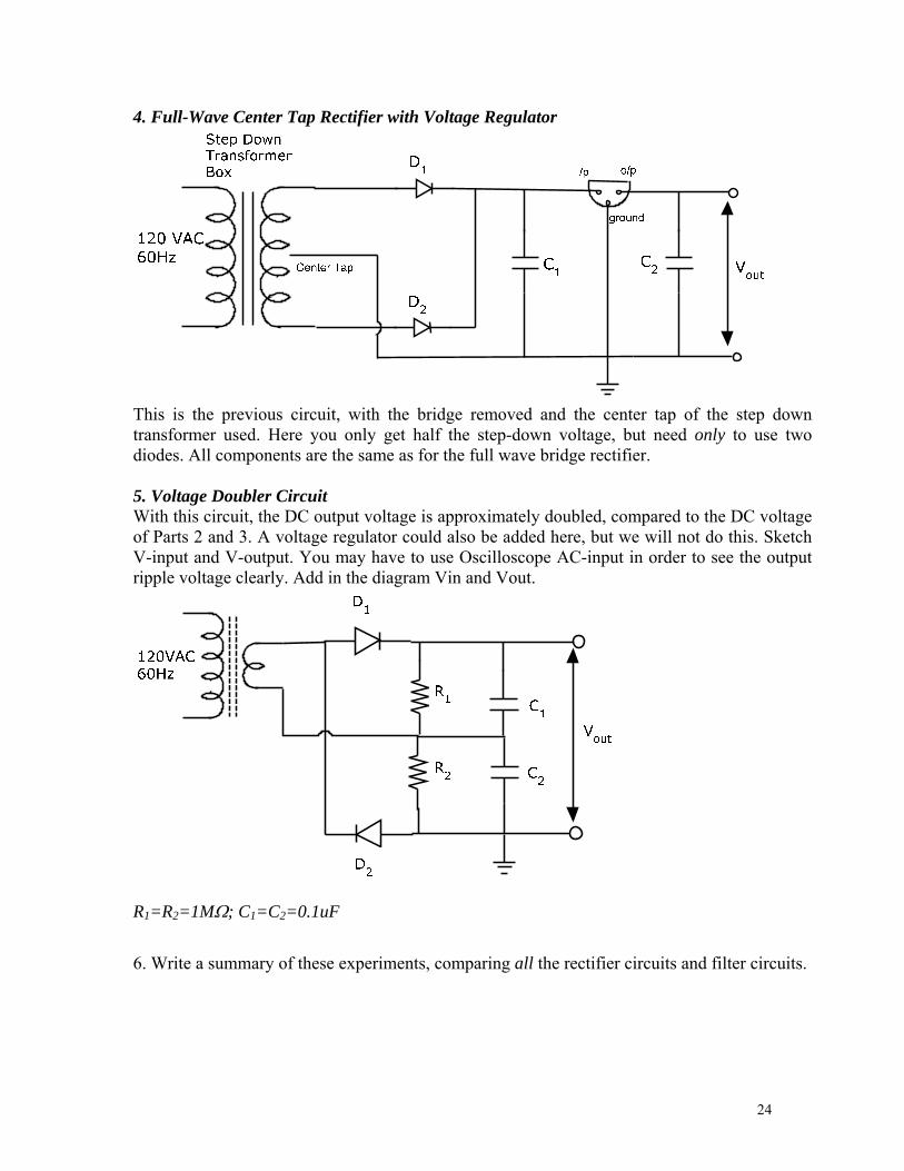
4. Full-Wave Center Tap Rectifier with Voltage Regulator
This is the previous circuit, with the bridge removed and the center tap of the step down transformer used. Here you only get half the step-down voltage, but need only to use two diodes. All components are the same as for the full wave bridge rectifier. 5. Voltage Doubler Circuit With this circuit, the DC output voltage is approximately doubled, compared to the DC voltage of Parts 2 and 3. A voltage regulator could also be added here, but we will not do this. Sketch V-input and V-output. You may have to use Oscilloscope AC-input in order to see the output ripple voltage clearly. Add in the diagram Vin and Vout.
R1=R2=1M; C1=C2=0.1uF
6. Write a summary of these experiments, comparing all the rectifier circuits and filter circuits.
25
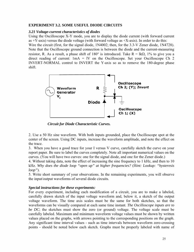
EXPERIMENT 3.2. SOME USEFUL DIODE CIRCUITS
3.21 Voltage-current characteristics of diodes Using the Oscilloscope X-Y mode, you are to display the diode current (with forward current as +Y-axis) versus the diode voltage (with forward voltage as +X-axis). In order to do this: Wire the circuit (first, for the signal diode, 1N4002; then, for the 3.3-V Zener diode, 1N4728). Note that the Oscilloscope ground connection is between the diode and the current-measuring resistor, R. As a result, a phase shift of 180° is introduced. Take R = lk, 1% to give you a direct reading of current: 1mA = lV on the Oscilloscope. Set your Oscilloscope Ch 2 INVERT-NORMAL control to INVERT the Y-axis so as to remove the 180-degree phase shift.
Circuit for Diode Characteristic Curves.
2. Use a 50 Hz sine waveform. With both inputs grounded, place the Oscilloscope spot at the center of the screen. Using DC inputs, increase the waveform amplitude, and note the effect on the trace. 3. When you have a good trace for your I versus V curve, carefully sketch the curve on your report paper. Be sure to label the curves completely. Note all important numerical values on the curves. (You will have two curves: one for the signal diode, and one for the Zener diode.) 4. Without taking data, note the effect of increasing the sine frequency to 1 kHz, and then to 10 kHz. Why does the diode loop “open up” at higher frequencies? (Hint: Lookup: “hysteresis loop”). 5. Write short summary of your observations. In the remaining experiments, you will observe the input/output waveforms of several diode circuits. Special instructions for these experiments: For every experiment, including each modification of a circuit, you are to make a labeled, carefully drawn sketch of the input voltage waveform and, below it, a sketch of the output voltage waveform. The time axis scales must be the same for both sketches, so that the waveforms can be visually compared at each same time instant. The Oscilloscope inputs are to be DC; the sketches must show the zero (or ground) voltage. The voltage scale must be carefully labeled. Maximum and minimum waveform voltage values must be shown by written values placed on the graphs, with arrows pointing to the corresponding positions on the graph. Any significant time interval values - such as time intervals between waveform zero-crossing points - should be noted below each sketch. Graphs must be properly labeled with name of
26
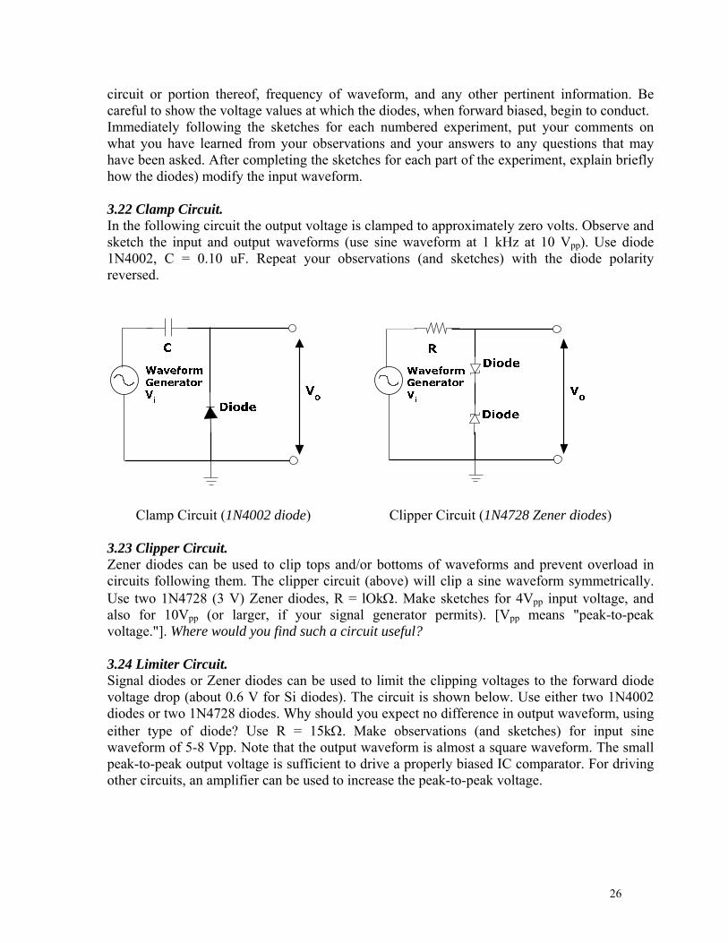
circuit or portion thereof, frequency of waveform, and any other pertinent information. Be careful to show the voltage values at which the diodes, when forward biased, begin to conduct. Immediately following the sketches for each numbered experiment, put your comments on what you have learned from your observations and your answers to any questions that may have been asked. After completing the sketches for each part of the experiment, explain briefly how the diodes) modify the input waveform. 3.22 Clamp Circuit. In the following circuit the output voltage is clamped to approximately zero volts. Observe and sketch the input and output waveforms (use sine waveform at 1 kHz at 10 Vpp). Use diode 1N4002, C = 0.10 uF. Repeat your observations (and sketches) with the diode polarity reversed.
Clamp Circuit (1N4002 diode) Clipper Circuit (1N4728 Zener diodes) 3.23 Clipper Circuit. Zener diodes can be used to clip tops and/or bottoms of waveforms and prevent overload in circuits following them. The clipper circuit (above) will clip a sine waveform symmetrically. Use two 1N4728 (3 V) Zener diodes, R = lOk. Make sketches for 4Vpp input voltage, and also for 10Vpp (or larger, if your signal generator permits). [Vpp means "peak-to-peak voltage."]. Where would you find such a circuit useful? 3.24 Limiter Circuit. Signal diodes or Zener diodes can be used to limit the clipping voltages to the forward diode voltage drop (about 0.6 V for Si diodes). The circuit is shown below. Use either two 1N4002 diodes or two 1N4728 diodes. Why should you expect no difference in output waveform, using either type of diode? Use R = 15k. Make observations (and sketches) for input sine waveform of 5-8 Vpp. Note that the output waveform is almost a square waveform. The small peak-to-peak output voltage is sufficient to drive a properly biased IC comparator. For driving other circuits, an amplifier can be used to increase the peak-to-peak voltage.
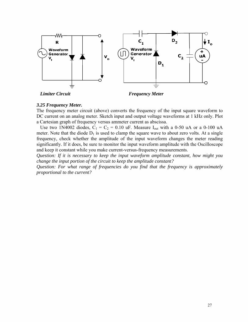
27
Limiter Circuit Frequency Meter 3.25 Frequency Meter. The frequency meter circuit (above) converts the frequency of the input square waveform to DC current on an analog meter. Sketch input and output voltage waveforms at 1 kHz only. Plot a Cartesian graph of frequency versus ammeter current as abscissa. Use two 1N4002 diodes, C1 = C2 = 0.10 uF. Measure Iout with a 0-50 uA or a 0-100 uA meter. Note that the diode D1 is used to clamp the square wave to about zero volts. At a single frequency, check whether the amplitude of the input waveform changes the meter reading significantly. If it does, be sure to monitor the input waveform amplitude with the Oscilloscope and keep it constant while you make current-versus-frequency measurements. Question: If it is necessary to keep the input waveform amplitude constant, how might you change the input portion of the circuit to keep the amplitude constant? Question: For what range of frequencies do you find that the frequency is approximately proportional to the current?
28
EXPERIMENT 4. SOME USEFUL TRANSISTOR CIRCUITS Object: To observe transistor function in the cutoff, linear and saturation regions. To observe the input/output waveforms of some transistor circuits. To measure low-frequency cutoff, input and output impedances of circuits. Special instructions: Use Engineer's Computation Pad sheets (National 42-583) for sketches and comments - one side of sheets only. 1. Copy each circuit on your paper. 2. Assemble each circuit in accord with the general instructions on measurement Procedures, EXP. 4 Appendix Page 4. Check your wiring carefully and set VCC power supply to correct voltage before attaching power leads to circuit board. 3. For every experiment, including each modification of a circuit, you are to make a labeled, carefully drawn sketch of the input voltage waveform and, below it, a sketch of the output voltage waveform. 3.1 The time axis must be the same for both sketches, so that the waveforms can be visually compared at each time instant. 3.2 The Oscilloscope inputs must be DC, unless otherwise specified; the sketches must show the zero (or ground) voltage. 3.3 The voltage and time scales must be carefully labeled. 3.4 Maximum and minimum voltages must be shown by written voltage values placed on the graphs with arrows pointing to the corresponding positions on the graph. 3.5 Any significant time interval values - such as time intervals between waveform zero-crossing points - should be noted below each sketch 3.6 Graphs must be properly labeled: name of circuit, or portion thereof; frequency of waveform; and any other pertinent information. Following the sketches) for each numbered experiment, place your comments on what you have learned from your observations and your answers to any questions that may have been asked. Carry out any other instructions given for an individual experiment. After completing the operations specified for each part of the experiment, write a short summary.
29
EXP. 4.1 Transistor Characteristic Curves. Only one laboratory station will be fitted out with a Cathode Ray Oscilloscope transistor curve tracer. You will have to share use of this CRO with others, so you may have to proceed with the remaining parts of the experiment while waiting to use the CRO. You are to display on the CRO the curves for the transistor (2N2222A, NPN) and sketch a reasonable facsimile on your paper. Label axes and curves. Determine from your sketch of the characteristic curves a value for the static forward current transfer ratio, hFE = IC/IB. Mark the points on your sketch that you used to determine this parameter. hFE is also called the static beta of the transistor. Using an arbitrary load resistance value, draw a load line on your graph. Show clearly on this line the cutoff point, the linear region and the saturation region. State the value of your load resistance. No further comment or summary is required for EXP. 4.1. Description of transistor saturation In most of our transistor circuits, the transistor is biased, and operated, so that the transistor is always between the saturation and the cut-off points. At both saturation and at cut-off, the collector current is no longer a linear function of the base current, and so these regions are avoided when linear amplification is desired. However, when current switching is desired, we deliberately drive the transistor from cut-off to saturation, and vice versa. Saturation in an NPN transistor is defined as the condition of the transistor when the base current and the collector current combine in such a way as to cause the collector voltage to drop below the base voltage. In this state, the three inter-electrode voltages, VBE, VBC and VCE, are all positive and all have values less than about one volt. Each of these voltages changes very little with large changes in IB (base current) and IC (collector current). [Such small inter-electrode voltage changes with changes in current are normally associated with forward-biased diodes in 2-terminal solid-state elements. Because of the internal structure of the transistor (very thin base thickness that separates the emitter and collector regions, and the different impurity doping of the emitter and collector regions), the similarity of inter-electrode behavior to diodes should not be pressed too far in attempts to explain the behavior of the transistor in saturation.] In the saturation region, because of the insensitivity of the inter-electrode voltages to IB and IC changes, the magnitude of IB is determined largely by its series resistor RB and its voltage supply VBB, independent of the magnitude of IC. In like manner, the magnitude of IC is determined largely by its series resistor RC and its voltage supply.
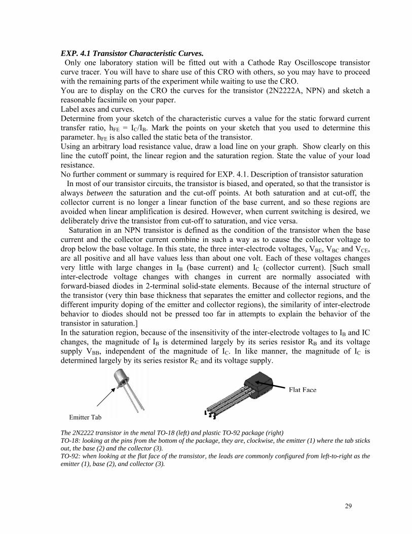
Emitter Tab The 2N2222 transistor in the metal TO-18 (left) and plastic TO-92 package (right) TO-18: looking at the pins from the bottom of the package, they are, clockwise, the emitter (1) where the tab sticks out, the base (2) and the collector (3). TO-92: when looking at the flat face of the transistor, the leads are commonly configured from left-to-right as the emitter (1), base (2), and collector (3).
Flat Face
30
Decade Box
D
Rc
B
C
E
Vcc
V1
RB
22k
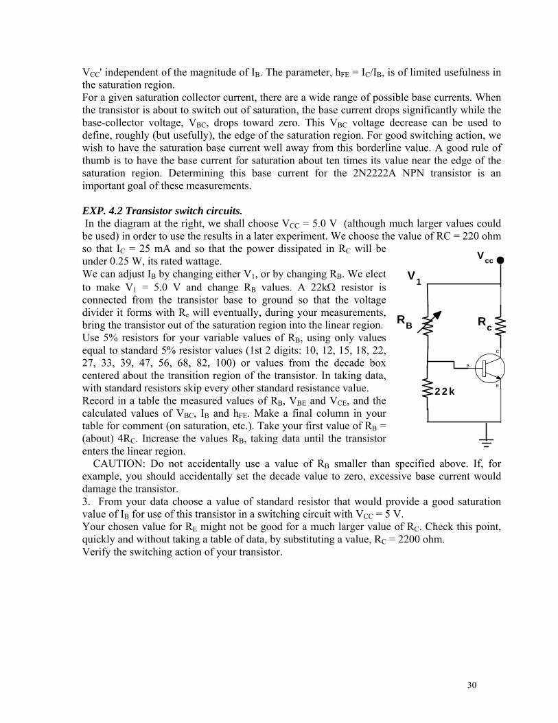
VCC' independent of the magnitude of IB. The parameter, hFE = IC/IB, is of limited usefulness in the saturation region. For a given saturation collector current, there are a wide range of possible base currents. When the transistor is about to switch out of saturation, the base current drops significantly while the base-collector voltage, VBC, drops toward zero. This VBC voltage decrease can be used to define, roughly (but usefully), the edge of the saturation region. For good switching action, we wish to have the saturation base current well away from this borderline value. A good rule of thumb is to have the base current for saturation about ten times its value near the edge of the saturation region. Determining this base current for the 2N2222A NPN transistor is an important goal of these measurements. EXP. 4.2 Transistor switch circuits. In the diagram at the right, we shall choose VCC = 5.0 V (although much larger values could be used) in order to use the results in a later experiment. We choose the value of RC = 220 ohm so that IC = 25 mA and so that the power dissipated in RC will be under 0.25 W, its rated wattage. We can adjust IB by changing either V1, or by changing RB. We elect to make V1 = 5.0 V and change RB values. A 22k resistor is connected from the transistor base to ground so that the voltage divider it forms with Re will eventually, during your measurements, bring the transistor out of the saturation region into the linear region. Use 5% resistors for your variable values of RB, using only values equal to standard 5% resistor values (1st 2 digits: 10, 12, 15, 18, 22, 27, 33, 39, 47, 56, 68, 82, 100) or values from the decade box centered about the transition region of the transistor. In taking data, with standard resistors skip every other standard resistance value. Record in a table the measured values of RB, VBE and VCE, and the calculated values of VBC, IB and hFE. Make a final column in your table for comment (on saturation, etc.). Take your first value of RB = (about) 4RC. Increase the values RB, taking data until the transistor enters the linear region. CAUTION: Do not accidentally use a value of RB smaller than specified above. If, for example, you should accidentally set the decade value to zero, excessive base current would damage the transistor. 3. From your data choose a value of standard resistor that would provide a good saturation value of IB for use of this transistor in a switching circuit with VCC = 5 V. Your chosen value for RE might not be good for a much larger value of RC. Check this point, quickly and without taking a table of data, by substituting a value, RC = 2200 ohm. Verify the switching action of your transistor.
31
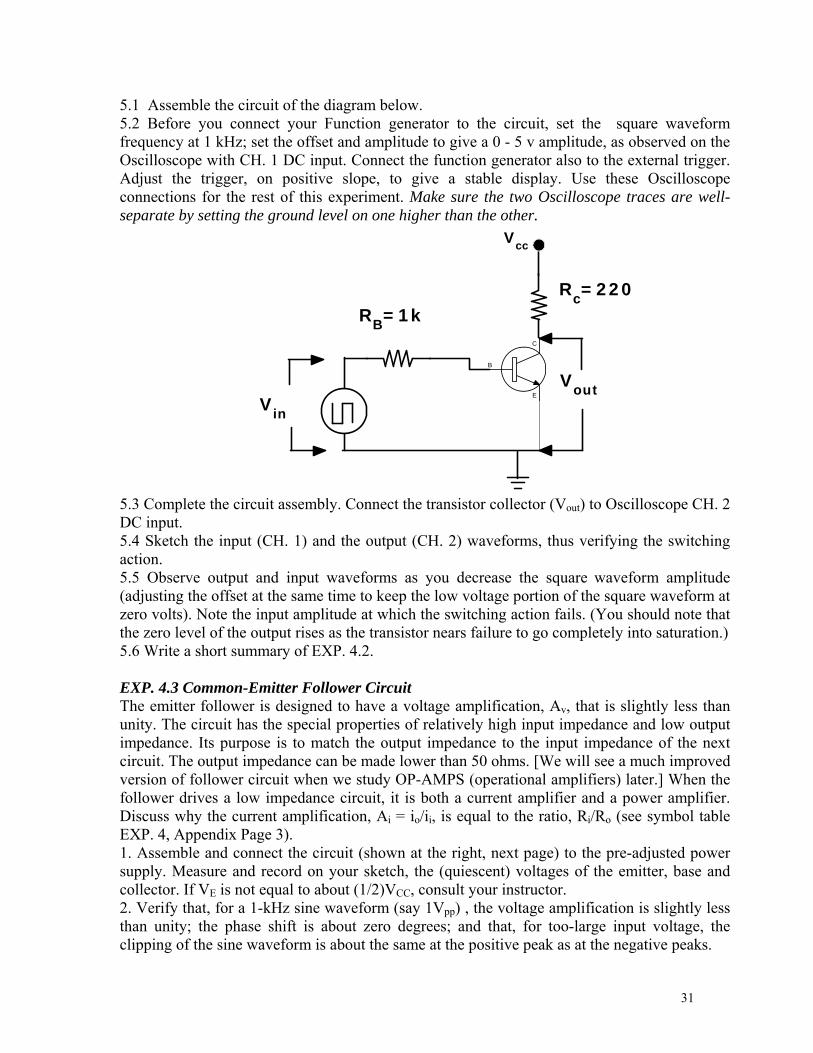
5.1 Assemble the circuit of the diagram below. 5.2 Before you connect your Function generator to the circuit, set the square waveform frequency at 1 kHz; set the offset and amplitude to give a 0 - 5 v amplitude, as observed on the Oscilloscope with CH. 1 DC input. Connect the function generator also to the external trigger. Adjust the trigger, on positive slope, to give a stable display. Use these Oscilloscope connections for the rest of this experiment. Make sure the two Oscilloscope traces are well-separate by setting the ground level on one higher than the other.
Decade Box
D
Rc=220
B
C
E
Vout
RB=1k
Vcc
Vin
5.3 Complete the circuit assembly. Connect the transistor collector (Vout) to Oscilloscope CH. 2 DC input. 5.4 Sketch the input (CH. 1) and the output (CH. 2) waveforms, thus verifying the switching action. 5.5 Observe output and input waveforms as you decrease the square waveform amplitude (adjusting the offset at the same time to keep the low voltage portion of the square waveform at zero volts). Note the input amplitude at which the switching action fails. (You should note that the zero level of the output rises as the transistor nears failure to go completely into saturation.) 5.6 Write a short summary of EXP. 4.2. EXP. 4.3 Common-Emitter Follower Circuit The emitter follower is designed to have a voltage amplification, Av, that is slightly less than unity. The circuit has the special properties of relatively high input impedance and low output impedance. Its purpose is to match the output impedance to the input impedance of the next circuit. The output impedance can be made lower than 50 ohms. [We will see a much improved version of follower circuit when we study OP-AMPS (operational amplifiers) later.] When the follower drives a low impedance circuit, it is both a current amplifier and a power amplifier. Discuss why the current amplification, Ai = io/ii, is equal to the ratio, Ri/Ro (see symbol table EXP. 4, Appendix Page 3). 1. Assemble and connect the circuit (shown at the right, next page) to the pre-adjusted power supply. Measure and record on your sketch, the (quiescent) voltages of the emitter, base and collector. If VE is not equal to about (1/2)VCC, consult your instructor. 2. Verify that, for a 1-kHz sine waveform (say 1Vpp) , the voltage amplification is slightly less than unity; the phase shift is about zero degrees; and that, for too-large input voltage, the clipping of the sine waveform is about the same at the positive peak as at the negative peaks.
32
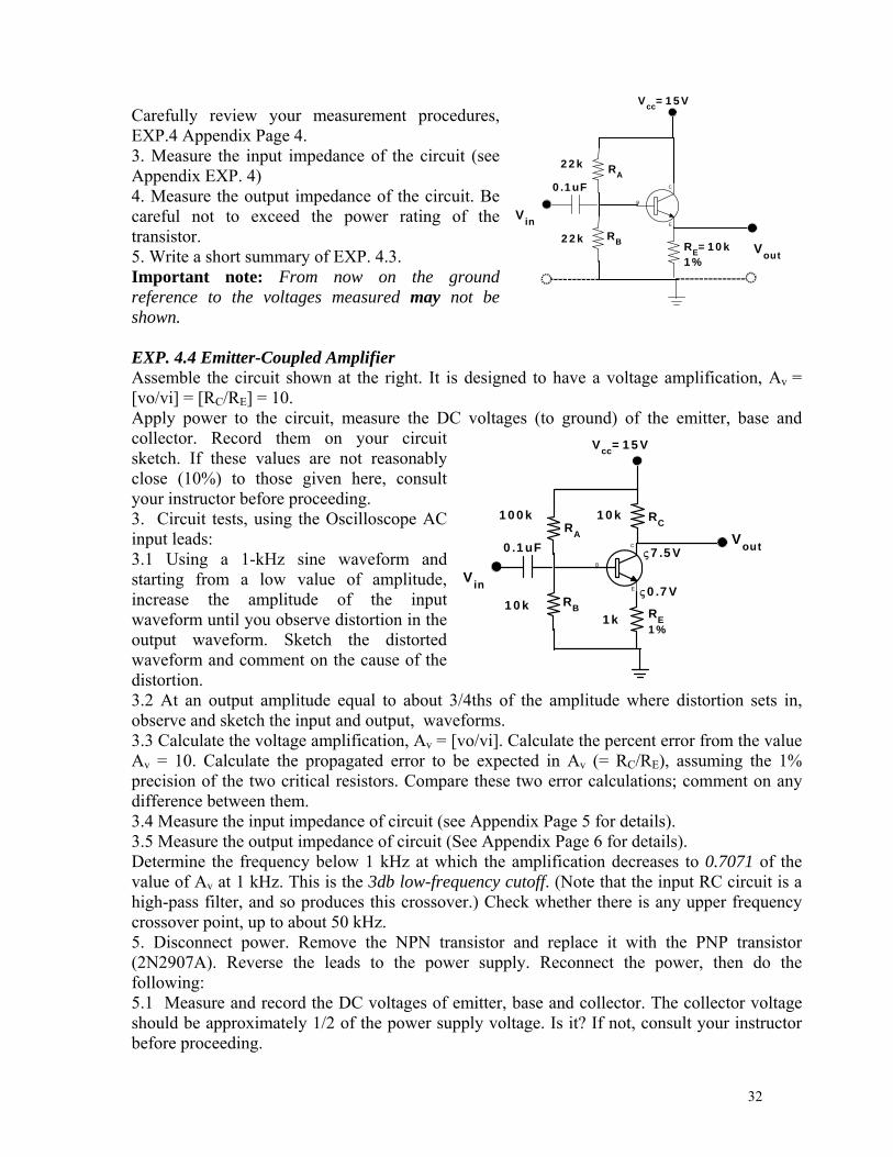
Carefully review your measurement procedures, EXP.4 Appendix Page 4. 3. Measure the input impedance of the circuit (see Appendix EXP. 4) 4. Measure the output impedance of the circuit. Be careful not to exceed the power rating of the transistor. 5. Write a short summary of EXP. 4.3. Important note: From now on the ground reference to the voltages measured may not be shown. EXP. 4.4 Emitter-Coupled Amplifier Assemble the circuit shown at the right. It is designed to have a voltage amplification, Av = [vo/vi] = [RC/RE] = 10. Apply power to the circuit, measure the DC voltages (to ground) of the emitter, base and collector. Record them on your circuit sketch. If these values are not reasonably close (10%) to those given here, consult your instructor before proceeding. 3. Circuit tests, using the Oscilloscope AC input leads: 3.1 Using a 1-kHz sine waveform and starting from a low value of amplitude, increase the amplitude of the input waveform until you observe distortion in the output waveform. Sketch the distorted waveform and comment on the cause of the distortion. 3.2 At an output amplitude equal to about 3/4ths of the amplitude where distortion sets in, observe and sketch the input and output, waveforms. 3.3 Calculate the voltage amplification, Av = [vo/vi]. Calculate the percent error from the value Av = 10. Calculate the propagated error to be expected in Av (= RC/RE), assuming the 1% precision of the two critical resistors. Compare these two error calculations; comment on any difference between them. 3.4 Measure the input impedance of circuit (see Appendix Page 5 for details). 3.5 Measure the output impedance of circuit (See Appendix Page 6 for details). Determine the frequency below 1 kHz at which the amplification decreases to 0.7071 of the value of Av at 1 kHz. This is the 3db low-frequency cutoff. (Note that the input RC circuit is a high-pass filter, and so produces this crossover.) Check whether there is any upper frequency crossover point, up to about 50 kHz. 5. Disconnect power. Remove the NPN transistor and replace it with the PNP transistor (2N2907A). Reverse the leads to the power supply. Reconnect the power, then do the following: 5.1 Measure and record the DC voltages of emitter, base and collector. The collector voltage should be approximately 1/2 of the power supply voltage. Is it? If not, consult your instructor before proceeding.
Decade Box
D
B
C
E
Vout
22kRE=10k1%
22k
Vin
Vcc=15V
RB
RA
0.1uF
Decade Box
DVout
10kRE1%
100k
Vin
Vcc=15V
RB
RA
RC10k
0.7V
7.5V
1k
0.1uFB
C
E
33
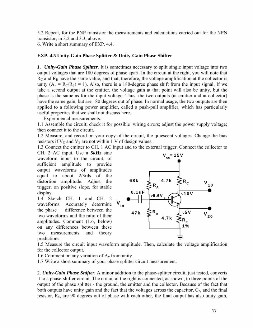
5.2 Repeat, for the PNP transistor the measurements and calculations carried out for the NPN transistor, in 3.2 and 3.3, above. 6. Write a short summary of EXP. 4.4. EXP. 4.5 Unity-Gain Phase Splitter & Unity-Gain Phase Shifter 1. Unity-Gain Phase Splitter. It is sometimes necessary to split single input voltage into two output voltages that are 180 degrees of phase apart. In the circuit at the right, you will note that RC and RE have the same value, and that, therefore, the voltage amplification at the collector is unity (Av = RC/RE) = 1). Also, there is a 180-degree phase shift from the input signal. If we take a second output at the emitter, the voltage gain at that point will also be unity, but the phase is the same as for the input voltage. Thus, the two outputs (at emitter and at collector) have the same gain, but are 180 degrees out of phase. In normal usage, the two outputs are then applied to a following power amplifier, called a push-pull amplifier, which has particularly useful properties that we shall not discuss here. Experimental measurements: 1.1 Assemble the circuit; check it for possible wiring errors; adjust the power supply voltage; then connect it to the circuit. 1.2 Measure, and record on your copy of the circuit, the quiescent voltages. Change the bias resistors if VC and VE are not within 1 V of design values. 1.3 Connect the emitter to CH. 1 AC input and to the external trigger. Connect the collector to CH. 2 AC input. Use a 5kHz sine waveform input to the circuit, of sufficient amplitude to provide output waveforms of amplitudes equal to about 2/3rds of the distortion amplitude. Adjust the trigger, on positive slope, for stable display. 1.4 Sketch CH. 1 and CH. 2 waveforms. Accurately determine the phase difference between the two waveforms and the ratio of their amplitudes. Comment (1.6, below) on any differences between these two measurements and theory predictions. 1.5 Measure the circuit input waveform amplitude. Then, calculate the voltage amplification for the collector output. 1.6 Comment on any variation of Av from unity. 1.7 Write a short summary of your phase-splitter circuit measurement. 2. Unity-Gain Phase Shifter. A minor addition to the phase-splitter circuit, just tested, converts it to a phase-shifter circuit. The circuit at the right is connected, as shown, to three points of the output of the phase splitter - the ground, the emitter and the collector. Because of the fact that both outputs have unity gain and the fact that the voltages across the capacitor, C2, and the final resistor, R5, are 90 degrees out of phase with each other, the final output has also unity gain,
Decade Box
D
V2047k
RE1%
68k
Vin
Vcc=15V
RB
RA
RC4.7k
5V
10V
4.7k
0.1uF
V10
5.6VB
C
E
34
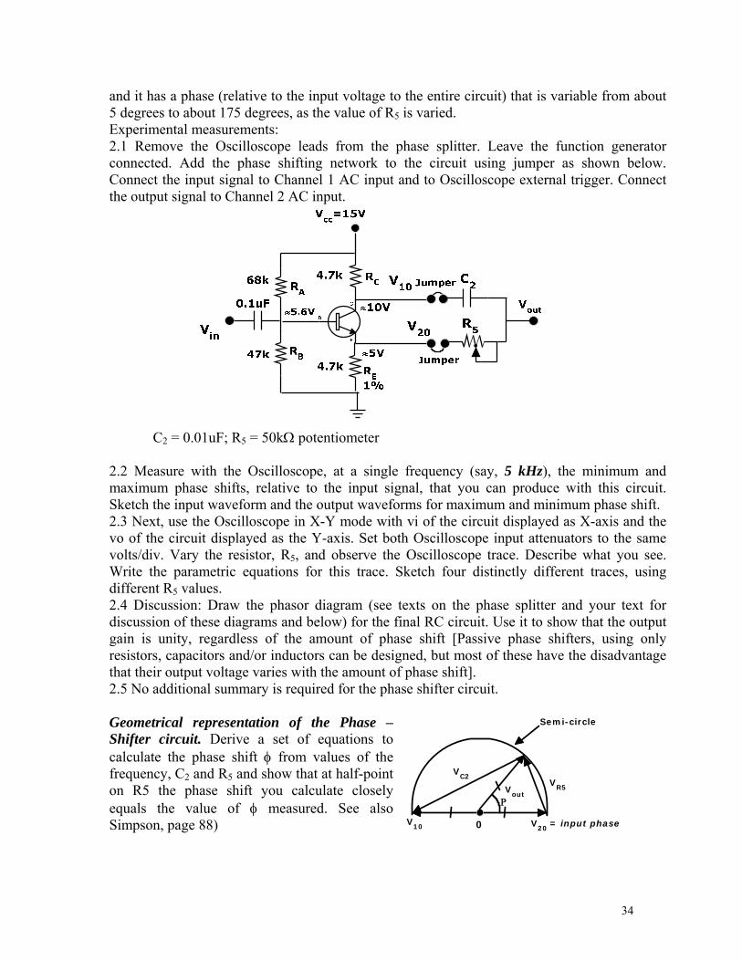
and it has a phase (relative to the input voltage to the entire circuit) that is variable from about 5 degrees to about 175 degrees, as the value of R5 is varied. Experimental measurements: 2.1 Remove the Oscilloscope leads from the phase splitter. Leave the function generator connected. Add the phase shifting network to the circuit using jumper as shown below. Connect the input signal to Channel 1 AC input and to Oscilloscope external trigger. Connect the output signal to Channel 2 AC input.
C2 = 0.01uF; R5 = 50k potentiometer
2.2 Measure with the Oscilloscope, at a single frequency (say, 5 kHz), the minimum and maximum phase shifts, relative to the input signal, that you can produce with this circuit. Sketch the input waveform and the output waveforms for maximum and minimum phase shift. 2.3 Next, use the Oscilloscope in X-Y mode with vi of the circuit displayed as X-axis and the vo of the circuit displayed as the Y-axis. Set both Oscilloscope input attenuators to the same volts/div. Vary the resistor, R5, and observe the Oscilloscope trace. Describe what you see. Write the parametric equations for this trace. Sketch four distinctly different traces, using different R5 values. 2.4 Discussion: Draw the phasor diagram (see texts on the phase splitter and your text for discussion of these diagrams and below) for the final RC circuit. Use it to show that the output gain is unity, regardless of the amount of phase shift [Passive phase shifters, using only resistors, capacitors and/or inductors can be designed, but most of these have the disadvantage that their output voltage varies with the amount of phase shift]. 2.5 No additional summary is required for the phase shifter circuit. Geometrical representation of the Phase –Shifter circuit. Derive a set of equations to calculate the phase shift from values of the frequency, C2 and R5 and show that at half-point on R5 the phase shift you calculate closely equals the value of measured. See also Simpson, page 88)
0V10 V20 = input phase
VR5Vout
VC2
Semi-circle
35
APPENDIX EXPERIMENT 4 Absolute Maximum Ratings of the NPN silicon 2N2222A transistor Each transistor type has limitations on voltages, current and power dissipation that cannot be exceeded without permanent damage to the transistor (and quite likely, damage to associated circuit components). These limitations are called absolute maximum ratings, a phrase that has obvious meaning. The following are taken from the manufacturer's data sheets. collector-base voltage (breakdown) 75 V collector-emitter voltage (breakdown) 40 V (IC = 0-500 mA, IBE = 0) emitter-base voltage (breakdown) 6 V continuous collector current 800 mA continuous power dissipation 500 mW (@ 25°C free air temp.) continuous power dissipation 1800 mW (@ 25°C CASE temp.) operating collector junction temp. -65 to 175°C soldering) lead temperature 230°C (1/16" from case for l0s) Absolute Maximum Ratings of the PNP silicon 2N2907A Transistor (PNP) Each transistor type has limitations on voltages, current and power dissipation that cannot be exceeded without permanent damage to the transistor (and quite likely, damage to associated circuit components). These limitations are called absolute maximum ratings, a phrase that has obvious meaning. The following are taken from the manufacturer's data sheets. collector-base voltage (breakdown) -60 V collector-emitter voltage (breakdown) -60 V (IC =0-100 mA, IBE =0) emitter-base voltage (breakdown) -5 V continuous collector current -600 mA continuous power dissipation 400 mW (@ 25°C free air temp.) continuous power dissipation 1800 mW (@ 25°C CASE temp.) operating collector junction temp. -65 to 200°C (soldering) lead temperature 230°C (1/16" from case for l0s)
36
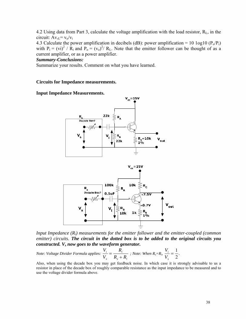
MEASUREMENT OF INPUT IMPEDANCE, OUTPUT IMPEDANCE, VOLTAGE AMPLIFICATION This discussion is given in the context of measuring the input impedance, output impedance and voltage amplification of the emitter follower circuit, for which, destruction of the transistor by heat is easily possible if precautions are not taken, as discussed below. The methods given can be adapted to other amplifier circuits with minor changes. Measurement Procedures The measurements must be carefully done, with care being given to the proper procedure to use in order to avoid serious errors. Refer to basic diagrams on Appendix Page 37-8. Specifically, the following must be done: Circuit assembly: circuits are to be assembled on the circuit board so that the layout of parts, the internal connections, and the input and output portions of the circuit are readily visible. Attention is to be given to the following: 1.1 ALL ground connections are to go to the bottom row of the board. 1.2 ALL Vcc connections are to go to the top row of the board. .3 Jumper wires are to be used to bring connections to circuit elements from awkward locations to other locations that will clearly permit a left-to-right sequence of circuit element input-to-output juxtaposition. 1.4 Jumper wires and bare-wire terminals are to be provided for the proper location and attachment of all external leads - power supply leads at top and bottom of board, input voltage leads at left side of board, Oscilloscope lead from input at left of transistor, Oscilloscope lead from output at right of transistor. 1.5 Measurements are to be made in such manner as to eliminate the high-pass filter effects of capacitors, unless you are instructed otherwise. 1.6 Measurements are to be made so as to eliminate the effects due to the internal resistance of the function generator. 1.7 To show that the above factors have been eliminated, the values of Av, Ri and R0 measured at 1 kHz and 10 kHz are to be compared. 2. Input resistance, Ri, is to be measured with no external load resistor, RL, connected to the circuit. 2.1 The input voltage, vi, applied to the circuit is to be measured with the Oscilloscope AC input terminal connected directly to the base of the transistor, following the input capacitor. 2.2 The input voltage, vi, is to be limited to 0.100 Vpp. The function generator amplitude may need adjustment to keep vi at a single value in all measurements. (This low value of input voltage will result in reasonable power dissipation in the transistor, as will be discussed below.) 2.3 In order that unwanted feedback from output to input be avoided, aim not to use the decade box in measuring the input or output resistance. Instead, opt to use one of the 1% resistors (10, 100, lk, l0k or 100k ohm, chosen to be of the order of the expected Ri), properly mounted an the circuit board. The input resistance can be calculated from this resistance value, Rs, and the measured values of input voltage, vs, and circuit input voltage, vi, as will be described below. To further reduce unwanted feedback, use shielded leads for all external connections to the circuit. You can determine Ri and R0 using the voltage divider formula (Pages 37-8). 2.4 If you note a high frequency oscillation of the circuit (which is due to positive feedback), connect a small capacitor (100 pF to 470 pF) from the input terminal of the circuit to ground. This will short out this high frequency oscillation. It may also be necessary (especially while measuring the output resistance) to connect another small capacitor between the output
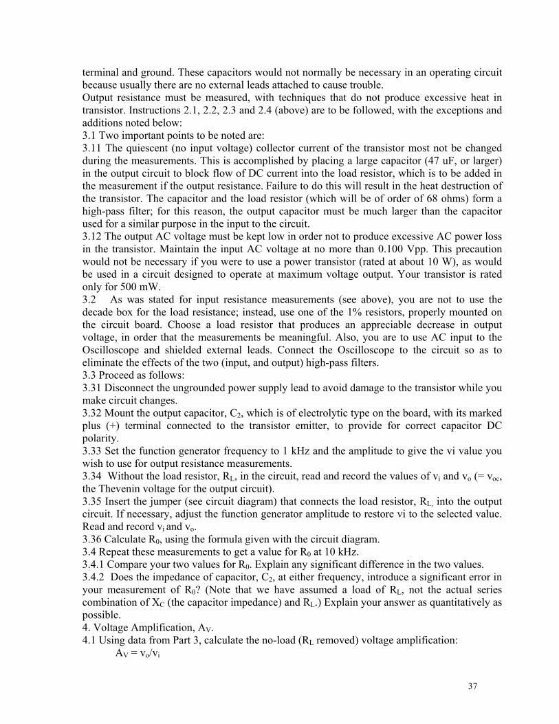
37
terminal and ground. These capacitors would not normally be necessary in an operating circuit because usually there are no external leads attached to cause trouble. Output resistance must be measured, with techniques that do not produce excessive heat in transistor. Instructions 2.1, 2.2, 2.3 and 2.4 (above) are to be followed, with the exceptions and additions noted below: 3.1 Two important points to be noted are: 3.11 The quiescent (no input voltage) collector current of the transistor most not be changed during the measurements. This is accomplished by placing a large capacitor (47 uF, or larger) in the output circuit to block flow of DC current into the load resistor, which is to be added in the measurement if the output resistance. Failure to do this will result in the heat destruction of the transistor. The capacitor and the load resistor (which will be of order of 68 ohms) form a high-pass filter; for this reason, the output capacitor must be much larger than the capacitor used for a similar purpose in the input to the circuit. 3.12 The output AC voltage must be kept low in order not to produce excessive AC power loss in the transistor. Maintain the input AC voltage at no more than 0.100 Vpp. This precaution would not be necessary if you were to use a power transistor (rated at about 10 W), as would be used in a circuit designed to operate at maximum voltage output. Your transistor is rated only for 500 mW. 3.2 As was stated for input resistance measurements (see above), you are not to use the decade box for the load resistance; instead, use one of the 1% resistors, properly mounted on the circuit board. Choose a load resistor that produces an appreciable decrease in output voltage, in order that the measurements be meaningful. Also, you are to use AC input to the Oscilloscope and shielded external leads. Connect the Oscilloscope to the circuit so as to eliminate the effects of the two (input, and output) high-pass filters. 3.3 Proceed as follows: 3.31 Disconnect the ungrounded power supply lead to avoid damage to the transistor while you make circuit changes. 3.32 Mount the output capacitor, C2, which is of electrolytic type on the board, with its marked plus (+) terminal connected to the transistor emitter, to provide for correct capacitor DC polarity. 3.33 Set the function generator frequency to 1 kHz and the amplitude to give the vi value you wish to use for output resistance measurements. 3.34 Without the load resistor, RL, in the circuit, read and record the values of vi and vo (= voc, the Thevenin voltage for the output circuit). 3.35 Insert the jumper (see circuit diagram) that connects the load resistor, RL, into the output circuit. If necessary, adjust the function generator amplitude to restore vi to the selected value. Read and record vi and vo. 3.36 Calculate R0, using the formula given with the circuit diagram. 3.4 Repeat these measurements to get a value for R0 at 10 kHz. 3.4.1 Compare your two values for R0. Explain any significant difference in the two values. 3.4.2 Does the impedance of capacitor, C2, at either frequency, introduce a significant error in your measurement of R0? (Note that we have assumed a load of RL, not the actual series combination of XC (the capacitor impedance) and RL.) Explain your answer as quantitatively as possible. 4. Voltage Amplification, AV. 4.1 Using data from Part 3, calculate the no-load (RL removed) voltage amplification:
AV = vo/vi
38
4.2 Using data from Part 3, calculate the voltage amplification with the load resistor, RL, in the circuit: Av,L= vo/vi 4.3 Calculate the power amplification in decibels (dB): power amplification = 10 1og10 (Po/Pi) with Pi = (vi)2 / Ri and Po = (vo)
2/ RL. Note that the emitter follower can be thought of as a current amplifier, or as a power amplifier. Summary-Conclusions: Summarize your results. Comment on what you have learned. Circuits for Impedance measurements. Input Impedance Measurements.
Input Impedance (Ri) measurements for the emitter follower and the emitter-coupled (common emitter) circuits. The circuit in the dotted box is to be added to the original circuits you constructed. Vs now goes to the waveform generator.
Note: Voltage Divider Formula applies: is
i
s
i
RR
R
V
V
; Note: When Rs=Ri, .
2
1
s
i
V
V
Also, when using the decade box you may get feedback noise. In which case it is strongly advisable to us a resistor in place of the decade box of roughly comparable resistance as the input impedance to be measured and to use the voltage divider formula above.
39
Output Impedance Measurements.
Output Impedance (R0) measurements for the emitter follower and the emitter-coupled (common emitter) circuits. The circuit in the dotted box is to be added to the original circuits you constructed. Vs now goes to the waveform generator. Since the output impedance is less than1k, you are advised to use a large C2 value and operate at a higher frequency than our usual 1kHz, i.e. use 5kHz frequency (make small Xc=1/2fC2). Also measure Voc before inserting the (shorting) jumper wire and then measuring Vout.
Note: Voltage Divider Formula applies: oL
o
oc
out
RR
R
V
V
; Note: When RL=R0, .
2
1
OC
out
V
V
Also, when using the decade box you may get feedback noise. In which case it is strongly advisable to us a resistor in place of the decade box of roughly comparable resistance as the output impedance to be measured and to use the voltage divider formula above.
40
EXP. 5 OPERATIONAL AMPLIFIER CIRCUITS Basic Feedback Theory The following basic feedback concepts, for use with op-amp circuits, are excerpted from your text references. Derivations for output voltage formulas for the various circuits are given in the text. Take notes while you study because, at the end of each set of circuit measurements, you are to include in your summary, the derivation of the applicable output voltage formula. The ideal operational amplifier (hereinafter called op-amp) has the following characteristics: 1. Infinite voltage gain 2. Infinite input impedance 3. Infinite bandwidth 4. Zero output impedance These defined properties lead to two important theorems, called the golden rules: Rule 1. No current flows in or out of the input terminals. Rule 2. When negative feedback is applied the differential input voltage is reduced to zero. Using the above rules, the equations relating the circuit output voltage (or current) to the circuit input voltage (or current) are easily (yes!) derived. In some circuits, the assumptions of infinite input impedance and/or zero output impedance must be relaxed in order to calculate input impedance or output impedance of the circuit. These derivations, most of which will be found in the text, will not be repeated in this manual. The necessary equations for calculating the output voltage in each case will be given with the circuit diagrams. The general theory of feedback is interesting, but it is not necessary for our derivations. The golden rules and Kirchhoff's two circuit laws are all that we require. Kirchhoff's laws are: 1. At any circuit node, the sum of the currents entering the node equals the sum of the currents leaving the node. A circuit node is any junction of 3, or more, wire connections. 2. Around any closed loop of a circuit, the algebraic sum of the potential differences across each loop element is zero. [For passive circuit elements - resistance, capacitance, inductance, most solid state elements - this potential difference is taken to be negative — if the passive element is (mentally) traversed in the same direction as the conventional positive current, and inversely. For active circuit elements - power supplies, function generators, etc. - the potential difference is taken positive if the active element is internally traversed from its negative output terminal to its positive output terminal, and inversely. Circuit Assembly Instructions Except when you are occasionally instructed otherwise, each student at a station is to assemble and test his/her own circuit. At any station having more than one student, the students are not partners in the experiment; they must equally share test equipment and construction work. Circuit assembly must be neat, and must be carried out following instructions given in lecture by the instructor, and in this manual. Your instructor will tell you to disassemble your circuit and start over if you fail to follow instructions. The basic assembly of the op-amp circuits is the same for all of the circuits you will test. Careful attention to this basic assembly - once completed and not disassembled until all experiments are completed - will save you much time :
41
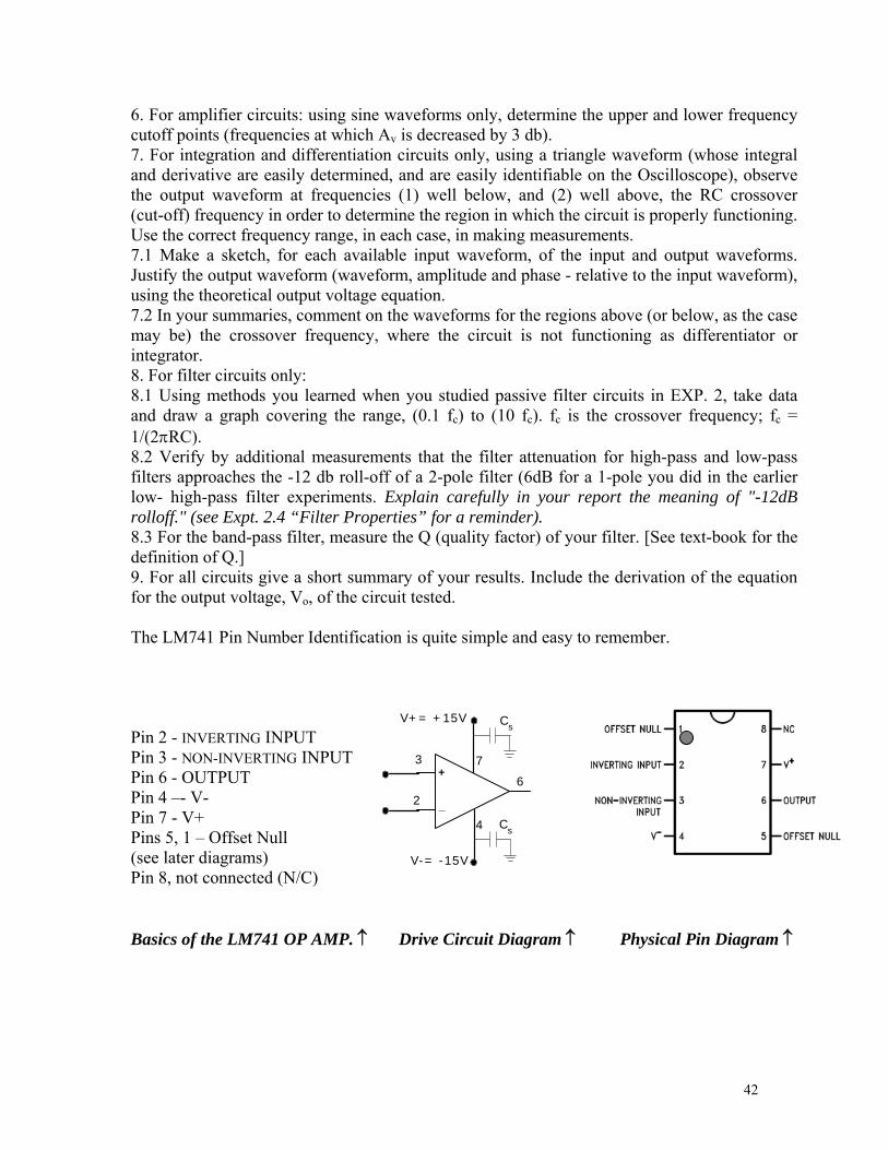
1. Place the 0.1 uF capacitors Cs, used to bypass power supply spikes to ground, as close to the op-amp terminals as possible. The uF value of these capacitors is not critical. 2. Place the 39-pF compensation capacitor as close to the op-amp terminals as possible. 3. Offset-null adjustments are to be made in some circuits, as discussed below. The output DC voltage level. should be zero in a circuit when the circuit input is shorted to ground. A suitably connected 50k potentiometer and a series 220k-ohm resistor will be used to bring the output to zero VDC, when needed. Preliminary circuit assembly 1. Assemble the basic op-amp circuit (power supply connections, ground connectionss shown in the Basic Circuit Diagram on Page 7. 2. Check your wiring carefully. 3. Before connecting to power supply plus and minus terminals, use a voltmeter or your Oscilloscope to set VCC= +15.0 V and VEE = -15.0 V. Turn off the power supply; then connect the power supply ground first, and then connect the plus and minus leads. It is alright to turn on and shut off the power supply while the op-amp is connected, as long as the voltage settings are correct. (Neither voltage must ever exceed 18 volts magnitude.) Also set the current limit (if available) to 1-2mA maximum. 4. Turn on the power supply. Shut it off fast if heat develops in your circuit, excessive heat means that you have made a serious wiring mistake. To test for heating, put your finger (lightly!) on the op-amp. It should feel cool, or slightly warm. 5. You are ready to proceed. NOTE WELL: The power supply voltages should be set in the above manner any time that you start a new day's experiments, or any time that you suspect the settings have been changed. It is well to check these voltages at your circuit nodes before you make any measurements. General Instructions for Experiments Draw the circuit diagram for the experiment, including the offset-null potentiometer and resistor, but omitting the rest of the basic circuit elements in the diagram on page 7. Turn off power supply. Assemble the rest of the circuit. Check wiring carefully. Turn on power. Check power supply voltages at the circuit nodes. Observe input voltage on Oscilloscope CH1 DC input; observe output voltage on Oscilloscope CH2 DC input; trigger on CH1. Adjust trigger LEVEL (usually, on positive slope) for a stable display. (Trigger on CH2 if CH1 input voltage does not give stable display. Record this fact whenever you do this.) Ground the circuit input voltage terminal with a short lead (exception: for a differential amplifier, short the 2 input terminals to each other with a short lead, but not to ground) and check the output voltage for zero offset. If applicable, adjust null-offset circuit. (Normally, this setting will be OK after the first adjustment.). Now un-short these leads. For all circuits except the active filters, check circuit response at 1 kHz for sine, triangle and square waveforms. Be sure to adjust the function generator output each time for suitable amplitude and for zero offset. 5.1 Increase the function generator amplitude in order to find the output voltage distortion point. Then decrease to about 3/4ths of this output amplitude so as to have an undistorted waveform. 5.2 Make labeled sketches of input and output waveforms for all three input waveforms. 5.3 For amplifier circuits, take necessary measurements and calculate Av = Vo/Vi 5.4 Measure input resistance and output resistance only if directed to do so later.
42
6. For amplifier circuits: using sine waveforms only, determine the upper and lower frequency cutoff points (frequencies at which Av is decreased by 3 db). 7. For integration and differentiation circuits only, using a triangle waveform (whose integral and derivative are easily determined, and are easily identifiable on the Oscilloscope), observe the output waveform at frequencies (1) well below, and (2) well above, the RC crossover (cut-off) frequency in order to determine the region in which the circuit is properly functioning. Use the correct frequency range, in each case, in making measurements. 7.1 Make a sketch, for each available input waveform, of the input and output waveforms. Justify the output waveform (waveform, amplitude and phase - relative to the input waveform), using the theoretical output voltage equation. 7.2 In your summaries, comment on the waveforms for the regions above (or below, as the case may be) the crossover frequency, where the circuit is not functioning as differentiator or integrator. 8. For filter circuits only: 8.1 Using methods you learned when you studied passive filter circuits in EXP. 2, take data and draw a graph covering the range, (0.1 fc) to (10 fc). fc is the crossover frequency; fc = 1/(2RC). 8.2 Verify by additional measurements that the filter attenuation for high-pass and low-pass filters approaches the -12 db roll-off of a 2-pole filter (6dB for a 1-pole you did in the earlier low- high-pass filter experiments. Explain carefully in your report the meaning of "-12dB rolloff." (see Expt. 2.4 “Filter Properties” for a reminder). 8.3 For the band-pass filter, measure the Q (quality factor) of your filter. [See text-book for the definition of Q.] 9. For all circuits give a short summary of your results. Include the derivation of the equation for the output voltage, Vo, of the circuit tested. The LM741 Pin Number Identification is quite simple and easy to remember. Pin 2 - INVERTING INPUT Pin 3 - NON-INVERTING INPUT Pin 6 - OUTPUT Pin 4 –- V- Pin 7 - V+ Pins 5, 1 – Offset Null (see later diagrams) Pin 8, not connected (N/C) Basics of the LM741 OP AMP. Drive Circuit Diagram Physical Pin Diagram
LM741CN2
6
3 7
4
V+= +15V
V-= -15V
Cs
Cs
LM741
+
_
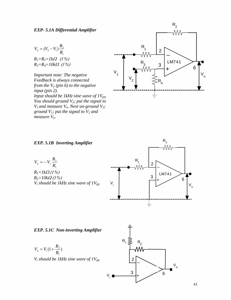
43
EXP- 5.1A Differential Amplifier
1
212 )(
R
RVVVo
R1=R3=1k R2=R4=10k Important note: The negative Feedback is always connected from the Vo (pin 6) to the negative input (pin 2). Input should be 1kHz sine wave of 1Vpp. You should ground V2; put the signal to V1 and measure Vo. Next un-ground V2; ground V1; put the signal to V2 and measure Vo. EXP. 5.1B Inverting Amplifier
1
2
R
RVV io
R1=1k R2=10kVi should be 1kHz sine wave of 1Vpp EXP. 5.1C Non-inverting Amplifier
)1(1
2
R
RVV io
Vi should be 1kHz sine wave of 1Vpp
LM741CN
2
63
R1
R2
Vi V
o
LM741
_
+
LM741CN
2
63R3
R4
R1
R2
V1V2
Vo
LM741
_
+
2
63
R1
Vi
LM741
_
+
R2
Vo
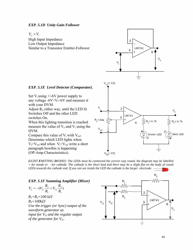
44
EXP. 5.1D Unity Gain Follower
io VV
High Input Impedance Low Output Impedance Similar to a Transistor Emitter-Follower EXP. 5.1E Level Detector (Comparator). Set Vi using +/-6V power supply to any voltage -6V<Vi<6V and measure it with your DVM. Adjust Ro either way, until the LED lit Switches Off and the other LED switches On. When this lighting transition is reached measure the value of Vo and Vi using the DVM. Compare this value of Vi with Vref. Determine which LED lights when Vi>Vref and when Vi<Vref write a short paragraph howthis is happening (OP-Amp Characteristics). LIGHT EMITTING DIODES: The LEDs must be connected the correct way round, the diagram may be labelled + for anode or - for cathode. The cathode is the short lead and there may be a slight flat on the body of round LEDs towards the cathode end. If you can see inside the LED the cathode is the larger electrode. EXP. 5.1F Summing Amplifier (Mixer)
)(1
32
1
31 R
RV
R
RVV iio
R1=R2=100 k R3=100k Use the trigger (or Sync) output of the waveform generator as input for Vi2 and the regular output of the generator for Vi1.
LM741CN
2
63
Vi
Vo
LM741
_
+
LM741CN
2
6
3R
o=50k
LM741
Vcc(+15)
VEE(-15)
Vi
R2=4.7kR1=4.7k
Red LEDGreen LED
Vref
+
_ Vo
-+
+-
LM741CN
2
63
R1
R2
Vi2
Vo
LM741Vi1 +
_
R3
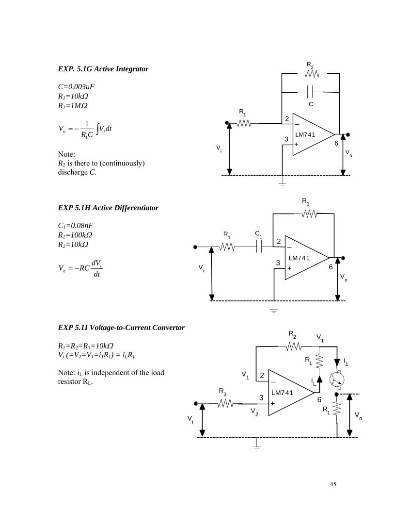
45
EXP. 5.1G Active Integrator C=0.003uF R1=10k R2=1M
dtVCR
V io 1
1
Note: R2 is there to (continuously) discharge C. EXP 5.1H Active Differentiator C1=0.08nF R1=100k R2=10k
dt
dVRCV i
o
EXP 5.1I Voltage-to-Current Convertor R1=R2=R3=10k Vi (=V2=V1=i1R1) = iLR1 Note: iL is independent of the load resistor RL.
LM741CN
2
63
R1
Vo
LM741
Vi
R2
C
+
_
LM741CN
2
63
R1
Vo
LM741Vi
R2
C1
+
_
LM741CN
2
63
Vo
LM741
Vi
R2
RL
R1
R3
i1
iLV1
V2
V1
+
_
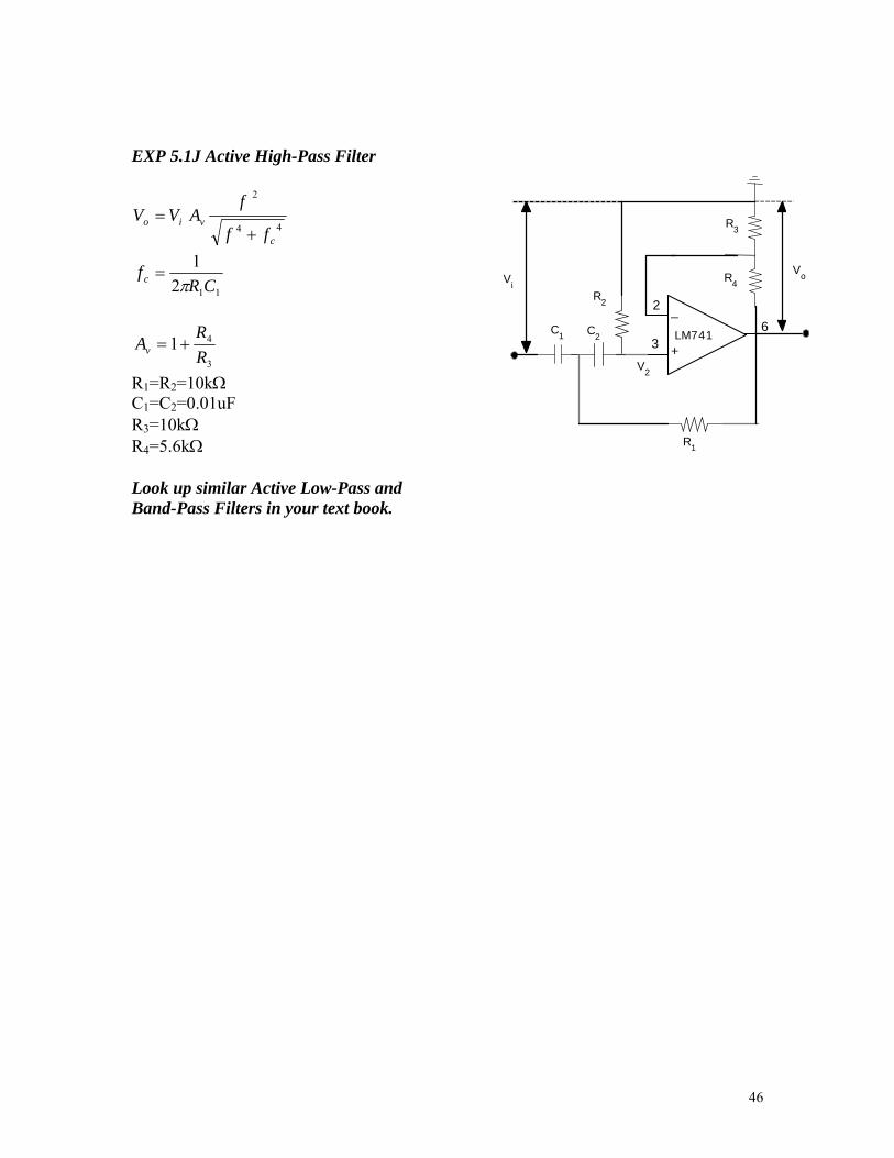
46
EXP 5.1J Active High-Pass Filter
44
2
c
vio
ff
fAVV
112
1
CRfc
3
41R
RAv
R1=R2=10k C1=C2=0.01uF R3=10k R4=5.6kLook up similar Active Low-Pass and Band-Pass Filters in your text book.
LM741CN
2
63
Vo
LM741
Vi
R1
R2
R3
V2
C1
R4
C2
+
_
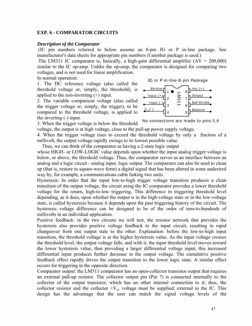
47
EXP. 6 - COMPARATOR CIRCUITS Description of the Comparator (IC pin numbers referred to below assume an 8-pin JG or P in-line package. See manufacturer's data sheets for appropriate pin numbers if another package is used.) The LM311 IC comparator is, basically, a high-gain differential amplifier (AV = 200,000) similar to the IC op-amp. Unlike the op-amp, the comparator is designed for comparing two voltages, and is not used for linear amplification. In normal operation: 1. The DC reference voltage (also called the threshold voltage or, simply, the threshold), is applied to the non-inverting (+) input. 2. The variable comparison voltage (also called the trigger voltage or, simply, the trigger), to be compared to the threshold voltage, is applied to the inverting (-) input. 3. When the trigger voltage is below the threshold voltage, the output is at high voltage, close to the pull-up power supply voltage. 4. When the trigger voltage rises to exceed the threshold voltage by only a fraction of a millivolt, the output voltage rapidly swings to its lowest possible value. Thus, we can think of the comparator as having a 2-state logic output whose HIGH- or LOW-LOGIC value depends upon whether the input analog trigger voltage is below, or above, the threshold voltage. Thus, the comparator serves as an interface between an analog and a logic circuit - analog input, logic output. The comparator can also be used to clean up (that is, restore to square-wave form) a digital signal that has been altered in some undesired way by, for example, a communications cable linking two units. Hysteresis: In order that the input low-to-high trigger voltage transition produces a clean transition of the output voltage, the circuit using the IC comparator provides a lower threshold voltage for the return, high-to-low triggering. This difference in triggering threshold level depending, as it does, upon whether the output is in the high-voltage state or in the low-voltage state, is called hysteresis because it depends upon the past triggering history of the circuit. The hysteresis voltage difference can be designed to be of the order of tens-to-hundreds of millivolts in an individual application. Positive feedback: in the two circuits we will test, the resistor network that provides the hysteresis also provides positive voltage feedback to the input circuit, resulting in rapid changeover from one output state to the other. Explanation: before the low-to-high input transition, the threshold voltage is at the higher hysteresis value. As the input voltage crosses the threshold level, the output voltage falls, and with it, the input threshold level moves toward the lower hysteresis value, thus providing a larger differential voltage input; this increased differential input produces further decrease in the output voltage. The cumulative positive feedback effect rapidly drives the output transition to the lower logic state. A similar effect occurs for triggering in the opposite direction. Comparator output: the LM311 comparator has an open-collector transistor output that requires an external pull-up resistor. The collector output pin (Pin 7) is connected internally to the collector of the output transistor, which has no other internal connection to it; thus, the collector resistor and the collector +Vcc voltage must be supplied, external to the IC. This design has the advantage that the user can match the signal voltage levels of the
No connections are made to pins 5,6
Vcc (+)
Output
Bal/Strobe
Balance
Emitter
Input (+)
Input (-)
Vcc(-)
1 8
2 7
3 6
4 5
LM311
JG or P in-line 8-pin Package
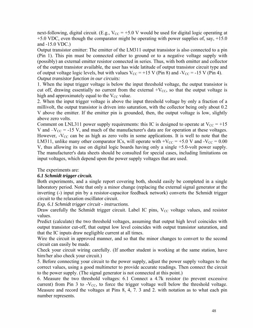
48
next-following, digital circuit. (E.g., VCC = +5.0 V would be used for digital logic operating at +5.0 VDC, even though the comparator might be operating with power supplies of, say, +15.0 and -15.0 VDC.) Output transistor emitter: The emitter of the LM311 output transistor is also connected to a pin (Pin 1). This pin must be connected either to ground or to a negative voltage supply with (possibly) an external emitter resistor connected in series. Thus, with both emitter and collector of the output transistor available, the user has wide latitude of output transistor circuit type and of output voltage logic levels, but with values VCC = +15 V (Pin 8) and -VCC = -15 V (Pin 4). Output transistor function in our circuits: 1. When the input trigger voltage is below the input threshold voltage, the output transistor is cut off, drawing essentially no current from the external +VCC, so that the output voltage is high and approximately equal to the VCC value. 2. When the input trigger voltage is above the input threshold voltage by only a fraction of a millivolt, the output transistor is driven into saturation, with the collector being only about 0.2 V above the emitter. If the emitter pin is grounded, then, the output voltage is low, slightly above zero volts. Comment on LNL311 power supply requirements: this IC is designed to operate at VCC = +15 V and –VCC = -15 V, and much of the manufacturer's data are for operation at these voltages. However, -VCC can be as high as zero volts in some applications. It is well to note that the LM311, unlike many other comparator ICs, will operate with +VCC = +5.0 V and -VCC = 0.00 V, thus allowing its use on digital logic boards having only a single +5.0-volt power supply. The manufacturer's data sheets should be consulted for special cases, including limitations on input voltages, which depend upon the power supply voltages that are used. The experiments are: 6.1 Schmidt trigger circuit. Both experiments, and a single report covering both, should easily be completed in a single laboratory period. Note that only a minor change (replacing the external signal generator at the inverting (-) input pin by a resistor-capacitor feedback network) converts the Schmidt trigger circuit to the relaxation oscillator circuit. Exp. 6.1 Schmidt trigger circuit - instructions. Draw carefully the Schmidt trigger circuit. Label IC pins, VCC voltage values, and resistor values. Predict (calculate) the two threshold voltages, assuming that output high level coincides with output transistor cut-off, that output low level coincides with output transistor saturation, and that the IC inputs draw negligible current at all times. Wire the circuit in approved manner, and so that the minor changes to convert to the second circuit can easily be made. Check your circuit wiring carefully. (If another student is working at the same station, have him/her also check your circuit.) 5. Before connecting your circuit to the power supply, adjust the power supply voltages to the correct values, using a good multimeter to provide accurate readings. Then connect the circuit to the power supply. (The signal generator is not connected at this point.) 6. Measure the two threshold voltages: 6.1 Connect a 4.7k resistor (to prevent excessive current) from Pin 3 to -VCC, to force the trigger voltage well below the threshold voltage. Measure and record the voltages at Pins 8, 4, 7. 3 and 2. with notation as to what each pin number represents.
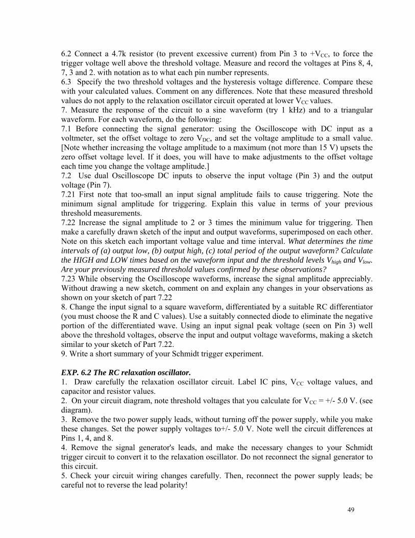
49
6.2 Connect a 4.7k resistor (to prevent excessive current) from Pin 3 to +VCC, to force the trigger voltage well above the threshold voltage. Measure and record the voltages at Pins 8, 4, 7, 3 and 2. with notation as to what each pin number represents. 6.3 Specify the two threshold voltages and the hysteresis voltage difference. Compare these with your calculated values. Comment on any differences. Note that these measured threshold values do not apply to the relaxation oscillator circuit operated at lower VCC values. 7. Measure the response of the circuit to a sine waveform (try 1 kHz) and to a triangular waveform. For each waveform, do the following: 7.1 Before connecting the signal generator: using the Oscilloscope with DC input as a voltmeter, set the offset voltage to zero VDC, and set the voltage amplitude to a small value. [Note whether increasing the voltage amplitude to a maximum (not more than 15 V) upsets the zero offset voltage level. If it does, you will have to make adjustments to the offset voltage each time you change the voltage amplitude.] 7.2 Use dual Oscilloscope DC inputs to observe the input voltage (Pin 3) and the output voltage (Pin 7). 7.21 First note that too-small an input signal amplitude fails to cause triggering. Note the minimum signal amplitude for triggering. Explain this value in terms of your previous threshold measurements. 7.22 Increase the signal amplitude to 2 or 3 times the minimum value for triggering. Then make a carefully drawn sketch of the input and output waveforms, superimposed on each other. Note on this sketch each important voltage value and time interval. What determines the time intervals of (a) output low, (b) output high, (c) total period of the output waveform? Calculate the HIGH and LOW times based on the waveform input and the threshold levels Vhigh and Vlow. Are your previously measured threshold values confirmed by these observations? 7.23 While observing the Oscilloscope waveforms, increase the signal amplitude appreciably. Without drawing a new sketch, comment on and explain any changes in your observations as shown on your sketch of part 7.22 8. Change the input signal to a square waveform, differentiated by a suitable RC differentiator (you must choose the R and C values). Use a suitably connected diode to eliminate the negative portion of the differentiated wave. Using an input signal peak voltage (seen on Pin 3) well above the threshold voltages, observe the input and output voltage waveforms, making a sketch similar to your sketch of Part 7.22. 9. Write a short summary of your Schmidt trigger experiment. EXP. 6.2 The RC relaxation oscillator. 1. Draw carefully the relaxation oscillator circuit. Label IC pins, VCC voltage values, and capacitor and resistor values. 2. On your circuit diagram, note threshold voltages that you calculate for VCC = +/- 5.0 V. (see diagram). 3. Remove the two power supply leads, without turning off the power supply, while you make these changes. Set the power supply voltages to+/- 5.0 V. Note well the circuit differences at Pins 1, 4, and 8. 4. Remove the signal generator's leads, and make the necessary changes to your Schmidt trigger circuit to convert it to the relaxation oscillator. Do not reconnect the signal generator to this circuit. 5. Check your circuit wiring changes carefully. Then, reconnect the power supply leads; be careful not to reverse the lead polarity!
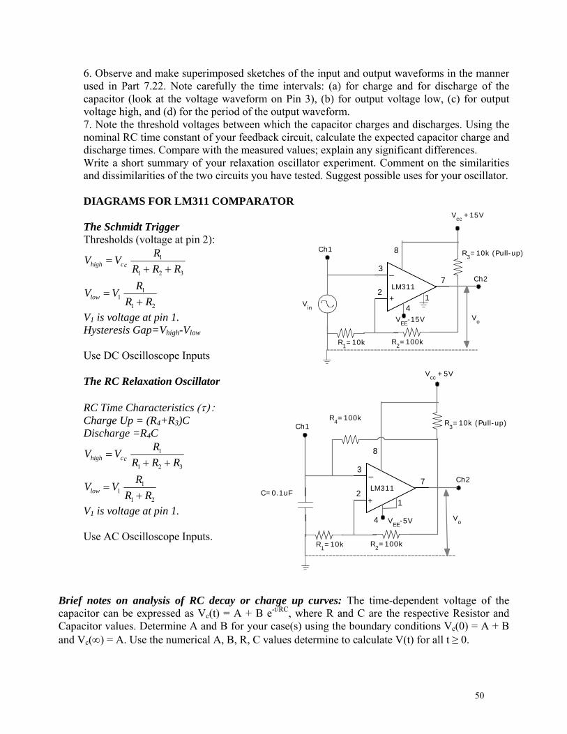
50
6. Observe and make superimposed sketches of the input and output waveforms in the manner used in Part 7.22. Note carefully the time intervals: (a) for charge and for discharge of the capacitor (look at the voltage waveform on Pin 3), (b) for output voltage low, (c) for output voltage high, and (d) for the period of the output waveform. 7. Note the threshold voltages between which the capacitor charges and discharges. Using the nominal RC time constant of your feedback circuit, calculate the expected capacitor charge and discharge times. Compare with the measured values; explain any significant differences. Write a short summary of your relaxation oscillator experiment. Comment on the similarities and dissimilarities of the two circuits you have tested. Suggest possible uses for your oscillator. DIAGRAMS FOR LM311 COMPARATOR The Schmidt Trigger Thresholds (voltage at pin 2):
21
11
321
1
RR
RVV
RRR
RVV
low
cchigh
V1 is voltage at pin 1. Hysteresis Gap=Vhigh-Vlow Use DC Oscilloscope Inputs The RC Relaxation Oscillator RC Time Characteristics Charge Up = (R4+R3)C Discharge =R4C
21
11
321
1
RR
RVV
RRR
RVV
low
cchigh
V1 is voltage at pin 1. Use AC Oscilloscope Inputs.
Brief notes on analysis of RC decay or charge up curves: The time-dependent voltage of the capacitor can be expressed as Vc(t) = A + B e-t/RC, where R and C are the respective Resistor and Capacitor values. Determine A and B for your case(s) using the boundary conditions Vc(0) = A + B and Vc() = A. Use the numerical A, B, R, C values determine to calculate V(t) for all t ≥ 0.
LM741CN
37
2
Ch1
Vo
LM311
Vin
Vcc +15V
14
8
VEE
-15V
R1=10k R2=100k
R3=10k (Pull-up)
Ch2_
+
LM741CN
37
2
Ch1
Vo
LM311C=0.1uF
Vcc +5V
1
4
8
VEE
-5V
R1=10k R2=100k
R3=10k (Pull-up)
Ch2
R4=100k
+
_
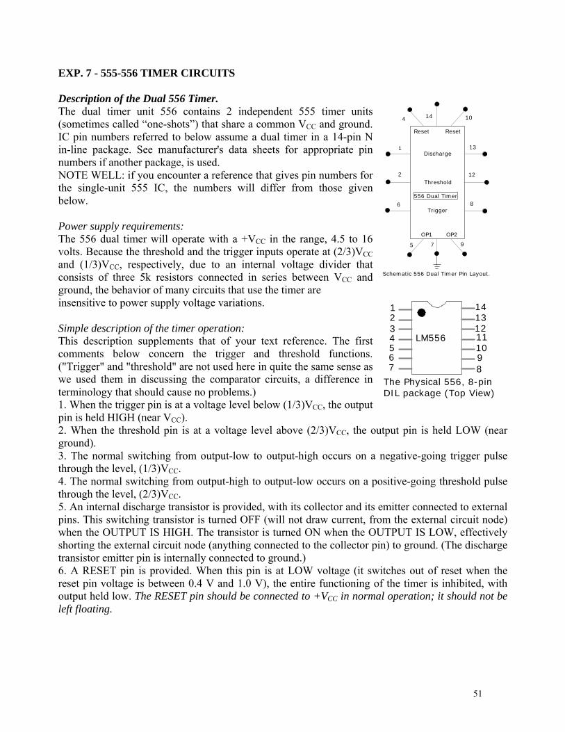
51
EXP. 7 - 555-556 TIMER CIRCUITS Description of the Dual 556 Timer. The dual timer unit 556 contains 2 independent 555 timer units (sometimes called “one-shots”) that share a common VCC and ground. IC pin numbers referred to below assume a dual timer in a 14-pin N in-line package. See manufacturer's data sheets for appropriate pin numbers if another package, is used. NOTE WELL: if you encounter a reference that gives pin numbers for the single-unit 555 IC, the numbers will differ from those given below. Power supply requirements: The 556 dual timer will operate with a +VCC in the range, 4.5 to 16 volts. Because the threshold and the trigger inputs operate at (2/3)VCC and (1/3)VCC, respectively, due to an internal voltage divider that consists of three 5k resistors connected in series between VCC and ground, the behavior of many circuits that use the timer are insensitive to power supply voltage variations. Simple description of the timer operation: This description supplements that of your text reference. The first comments below concern the trigger and threshold functions. ("Trigger" and "threshold" are not used here in quite the same sense as we used them in discussing the comparator circuits, a difference in terminology that should cause no problems.) 1. When the trigger pin is at a voltage level below (1/3)VCC, the output pin is held HIGH (near VCC). 2. When the threshold pin is at a voltage level above (2/3)VCC, the output pin is held LOW (near ground). 3. The normal switching from output-low to output-high occurs on a negative-going trigger pulse through the level, (1/3)VCC. 4. The normal switching from output-high to output-low occurs on a positive-going threshold pulse through the level, (2/3)VCC. 5. An internal discharge transistor is provided, with its collector and its emitter connected to external pins. This switching transistor is turned OFF (will not draw current, from the external circuit node) when the OUTPUT IS HIGH. The transistor is turned ON when the OUTPUT IS LOW, effectively shorting the external circuit node (anything connected to the collector pin) to ground. (The discharge transistor emitter pin is internally connected to ground.) 6. A RESET pin is provided. When this pin is at LOW voltage (it switches out of reset when the reset pin voltage is between 0.4 V and 1.0 V), the entire functioning of the timer is inhibited, with output held low. The RESET pin should be connected to +VCC in normal operation; it should not be left floating.
1
Reset
10
2
4
9
12
14
8
13
6
5
Trigger
OP1
Discharge
Threshold
Reset
OP2
7
556 Dual Timer
Schematic 556 Dual Timer Pin Layout.
1
121110987
65432
1413
LM556
The Physical 556, 8-pinDIL package (Top View)
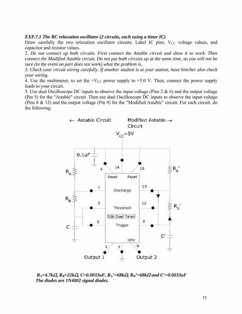
52
EXP.7.1 The RC relaxation oscillator (2 circuits, each using a timer IC) Draw carefully the two relaxation oscillator circuits. Label IC pins, VCC voltage values, and capacitor and resistor values. 2. Do not connect up both circuits. First connect the Astable circuit and show it to work. Then connect the Modified Astable circuit. Do not put both circuits up at the same time, as you will not be sure (in the event on part does not work) what the problem is. 3. Check your circuit wiring carefully. If another student is at your station, have him/her also check your wiring. 4. Use the multimeter, to set the +VCC power supply to +5.0 V. Then, connect the power supply leads to your circuit. 5. Use dual Oscilloscope DC inputs to observe the input voltage (Pins 2 & 6) and the output voltage (Pin 5) for the "Astable" circuit. Then use dual Oscilloscope DC inputs to observe the input voltage (Pins 8 & 12) and the output voltage (Pin 9) for the "Modified Astable" circuit. For each circuit, do the following.
RA=4.7kRB=22kC=0.0033uF, RA’=68k, RB’=68k and C’=0.0033uF The diodes are 1N4002 signal diodes.
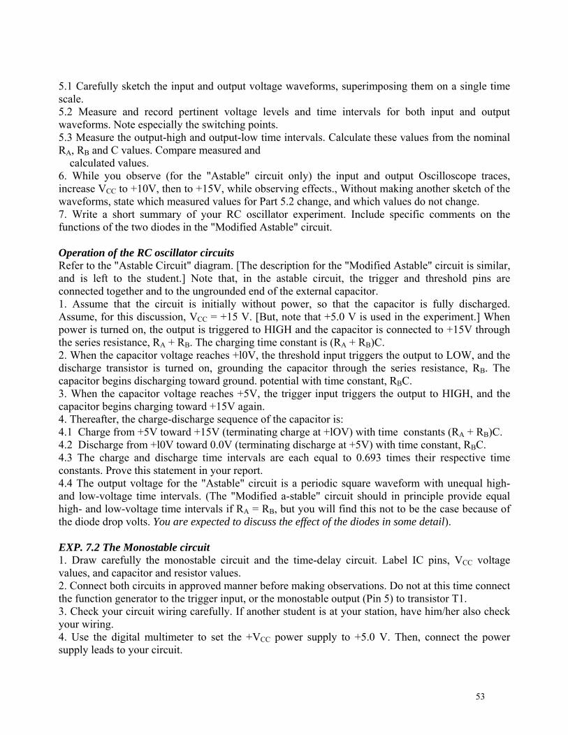
53
5.1 Carefully sketch the input and output voltage waveforms, superimposing them on a single time scale. 5.2 Measure and record pertinent voltage levels and time intervals for both input and output waveforms. Note especially the switching points. 5.3 Measure the output-high and output-low time intervals. Calculate these values from the nominal RA, RB and C values. Compare measured and calculated values. 6. While you observe (for the "Astable" circuit only) the input and output Oscilloscope traces, increase VCC to +10V, then to +15V, while observing effects., Without making another sketch of the waveforms, state which measured values for Part 5.2 change, and which values do not change. 7. Write a short summary of your RC oscillator experiment. Include specific comments on the functions of the two diodes in the "Modified Astable" circuit. Operation of the RC oscillator circuits Refer to the "Astable Circuit" diagram. [The description for the "Modified Astable" circuit is similar, and is left to the student.] Note that, in the astable circuit, the trigger and threshold pins are connected together and to the ungrounded end of the external capacitor. 1. Assume that the circuit is initially without power, so that the capacitor is fully discharged. Assume, for this discussion, VCC = +15 V. [But, note that +5.0 V is used in the experiment.] When power is turned on, the output is triggered to HIGH and the capacitor is connected to +15V through the series resistance, RA + RB. The charging time constant is (RA + RB)C. 2. When the capacitor voltage reaches +l0V, the threshold input triggers the output to LOW, and the discharge transistor is turned on, grounding the capacitor through the series resistance, RB. The capacitor begins discharging toward ground. potential with time constant, RBC. 3. When the capacitor voltage reaches +5V, the trigger input triggers the output to HIGH, and the capacitor begins charging toward +15V again. 4. Thereafter, the charge-discharge sequence of the capacitor is: 4.1 Charge from +5V toward +15V (terminating charge at +lOV) with time constants (RA + RB)C. 4.2 Discharge from +l0V toward 0.0V (terminating discharge at +5V) with time constant, RBC. 4.3 The charge and discharge time intervals are each equal to 0.693 times their respective time constants. Prove this statement in your report. 4.4 The output voltage for the "Astable" circuit is a periodic square waveform with unequal high- and low-voltage time intervals. (The "Modified a-stable" circuit should in principle provide equal high- and low-voltage time intervals if RA = RB, but you will find this not to be the case because of the diode drop volts. You are expected to discuss the effect of the diodes in some detail). EXP. 7.2 The Monostable circuit 1. Draw carefully the monostable circuit and the time-delay circuit. Label IC pins, VCC voltage values, and capacitor and resistor values. 2. Connect both circuits in approved manner before making observations. Do not at this time connect the function generator to the trigger input, or the monostable output (Pin 5) to transistor T1. 3. Check your circuit wiring carefully. If another student is at your station, have him/her also check your wiring. 4. Use the digital multimeter to set the +VCC power supply to +5.0 V. Then, connect the power supply leads to your circuit.
54
5. Record in a table the DC voltages of Pins 1, 2, 6, 5, 7 and 10, 13, 12, 8, 9. Identify each pin function in the table. Check these voltages are expected voltages for the monostable state of the circuit. 6. Before you connect the function generator to the circuit, adjust it for a square waveform output of 0V to +4.0V, at a frequency of about 400 Hz. Then, connect the function generator output to the capacitor CD of the differentiating RC filter, to provide the negative-going trigger pulse to Pin 6. Note that both a negative pulse and a positive pulse are generated at Pin 6; only the negative pulse affects the circuit. Although it is not here necessary, a suitably connected signal diode could be used to remove the positive pulse.
RD=4.7kCD=0.01uFC1=0.01uF, R1 is varied (see text) C1=0.01uF R2 is varied (see text)C2=0.01uFRB should be less than 1k
7. Use dual Oscilloscope DC inputs to observe three waveforms (as described below) for the mono-stable circuit. "Observe" means you are to make careful, well-labeled sketches of the three waveforms, superimposing them so that their relative time scales-are evident. Make these sketches for ONLY ONE value of R1 (use 22k), using 0.01 uF for Cl. 7.1 Connect the output (Pin 5) to Oscilloscope, Channel 1 and trigger on CH1. Adjust the Oscilloscope trigger level for stable triggering on positive slope. Do not change this CH1 connection
55
or the triggering, except for the trigger level if the display becomes unstable, while completing your waveform sketches. 7.2 First, connect the trigger (Pin 6) and, second, the external capacitor (Pins 1 & 2) to Oscilloscope Channel 2 in order to observe their waveforms. 7.3 Check that the 400-Hz frequency of your square wave is not critical by slowly increasing the generator frequency until interference with the mono-stable circuit operation occurs. 7.4 Analog-to-digital (resistance-to-time) conversion: 7.41 Record in a table the following data: (Col. 1) nominal value of Rl, (Col. 2) value of Rl measured with a Beckman digital multi-meter, (Col. 3) Oscilloscope-measured mono-stable output-high time, and (Col. 4) calculated output-high time (1.10 R1Cl). 7.42 Take data for R1 = 4.7k, 15k, 22k, 47k, 68k and 100k. 7.43 Make a Cartesian graph of R1 (Col. 2) versus measured output-high time (Col. 3), as horizontal axis. What does this graph tell you? Obtain the slope of the graph in ohms/microsecond, as your calibration constant for the circuit. 8. Write a short summary of your monostable circuit experiment. Operation of the Mono-stable Circuit. This mono-stable circuit has a single stable state, with the output (Pin 5) at LOW voltage, zero volts. This state is assured by the positive voltage VCC applied to the trigger (Pin 6) through the resistor RD, and by the zero voltage at the threshold (Pin 2) produced by the timer's internal discharge transistor, which shorts Pin 2 and the external capacitor Cl to ground potential. The discharge transistor (acting as a switch) is always on (equivalent to a closed switch) when the output is low, and is always off (equivalent to an open switch) when the output pin is high. A trigger pulse that is sufficiently negative-going to bring the trigger pin just below (1/3)VCC causes the circuit to switch to the state of output HIGH for the time interval, 1.10 R1C1, after which the circuit returns to its mono-stable state of output LOW until the next trigger pulse arrives. The trigger pulse produces the following sequence of events: 1. The output (Pin 5) immediately goes HIGH; 2. The discharge transistor turns off (removing the short to ground potential), allowing capacitor C1 to start charging toward VCC through resistor Rl. The threshold (Pin 1) is connected to Cl, and so its voltage also moves toward VCC. 3. When the capacitor-threshold voltage reaches (2/3)VCC, the output pin returns to its stable zero-volts state and the discharge transistor is turned on. 4. The discharge transistor effectively shorts Cl to ground and holds it and the threshold (Pin 1) at zero volts, thus completing the return of the circuit to its mono-stable state. In your report, prove that the length of the output-HIGH state is indeed equal to (1.10)R1C1. Note that 1.10 = -ln(1/3). The fact that a short, negative-going input trigger results in an output-high pulse, of duration that is proportional to the resistance R1, permits use of this circuit to convert a physical analog resistance measurement into a digital number. This is done by measuring the pulse length with a high speed digital timer, a simple feat for a computer module. The fact that many transducers convert such things as temperature changes, pressure changes, strain changes, etc. into resistance changes makes this circuit very useful in a wide range of analog-to-digital conversions. . EXP. 7.3 The Time-Delay circuit 1. Your time-delay circuit should already be wired, and the first mono-stable circuit should be functional so that its output pulse can be used to trigger the time-delay circuit. Replace the resistor
56
R1 by the value, 22k. Record, as part of your data for the time-delay circuit, your measured value of the first mono-stable output-high time for the 22k resistor. 2. Connect the output (Pin 5) of the mono-stable to the 470-ohm base resistor of the switching transistor Tl, as shown on the circuit diagram. 3. Connect the output (Pin 9) to Oscilloscope Channel 1 and trigger on CH1. Adjust the trigger level for stable triggering on positive slope. Do not change the CH1 connection or the triggering, except for the trigger level if the display becomes unstable, while completing your waveform sketches. 4. Connect the trigger, the threshold and the external capacitor (Pins 8 & 12) to Oscilloscope Channel 2 in order to observe the waveform. 5. With power on, R2=68k and the first monostable circuit providing the time-delay circuit trigger (the monostable, in turn, being triggered by the differentiated output of the function generator, as before), you should now be able to see a display that shows a delay of time, equal to the first monostable output-high time, before the capacitor C2 begins to charge (=1.10R2C2). During this time, the time-delay circuit output is high. The capacitor C2 then charges from zero toward 5.0 V with time constant, R2C2, while the time-delay output remains high. When the capacitor reaches (2/3)VCC, in time, 1.10 R2C2, the output triggers back to its zero-level monostable state. Sketch all waveforms carefully. 6. Verify that the time-delay output remains high for a time equal to the sum of the trigger pulse time (the output-high time of the first monostable circuit) and the charging time to (2/3)VCC of the capacitor C2. 7. Repeat 5-6 for R1 still fixed at 22k and R2 values of 22k, 47k, 100k and 220k. 8. Write a short summary of your time-delay circuit experiment. Description of the Time-Delay Circuit Refer to the circuit diagram. Note that this circuit, which is also a monostable circuit, differs from the first monostable circuit in two details. (1) The external capacitor and the threshold input are connected to the trigger input instead of to the discharge transistor, which is not used. (2) Before the external switching transistor T1 is triggered, it is initially biased to cutoff, allowing the capacitor and threshold input to rise above (2/3)VCC (actually, to about 4V), producing a stable output-LOW state. The sequence of operation follows: 1. The transistor Tl is turned on by an external, logical HIGH, triggering pulse that lasts for a duration determined by the circuit designer. This external transistor grounds the capacitor C2, quickly discharging it and forcing the trigger input (Pin 8) LOW, which in turn triggers the output (Pin 9) to the output-HIGH state. 2. The output-HIGH state continues until the external pulse turns transistor T1 off, then and only then allowing the capacitor C2 to charge from zero volts toward VCC through the series resistor R2, with time constant R2C2. The output-HIGH state continues for the additional time interval that is required for the capacitor to charge to (2/3)VCC, namely, 1.10R2C2. At this time, the circuit triggers back to its stable, output-LOW state. 3. Note that the total time of the output-HIGH state is the sum/of the external transistor on-time T1 and the R2C2 capacitor charging time. Thus, the RC timing is delayed until after the user's T1 on-time is terminated. 4. A convenient test source giving a known trigger pulse length is the output (Pin 5) of the first mono-stable circuit. Delay circuits similar to this one are used in microcomputers to delay RESET functions until power supplies have reached stable potentials

57
Final Comments The 555 single-unit timer and the 556 dual-unit timer have three fundamental operating modes. You have now wired and tested all three: 1. The free-running RC oscillator (the a-stable circuit and the modified a-stable circuit), 2. The mono-stable circuit, and 3. The time-delay circuit. Using these fundamental circuit types, experimenters have developed a wide range of interesting and useful circuits such as tachometers, burglar alarms, assorted time delay circuits, and generators of various audio sounds. The student is referred to applications notes of manufacturers for more details.
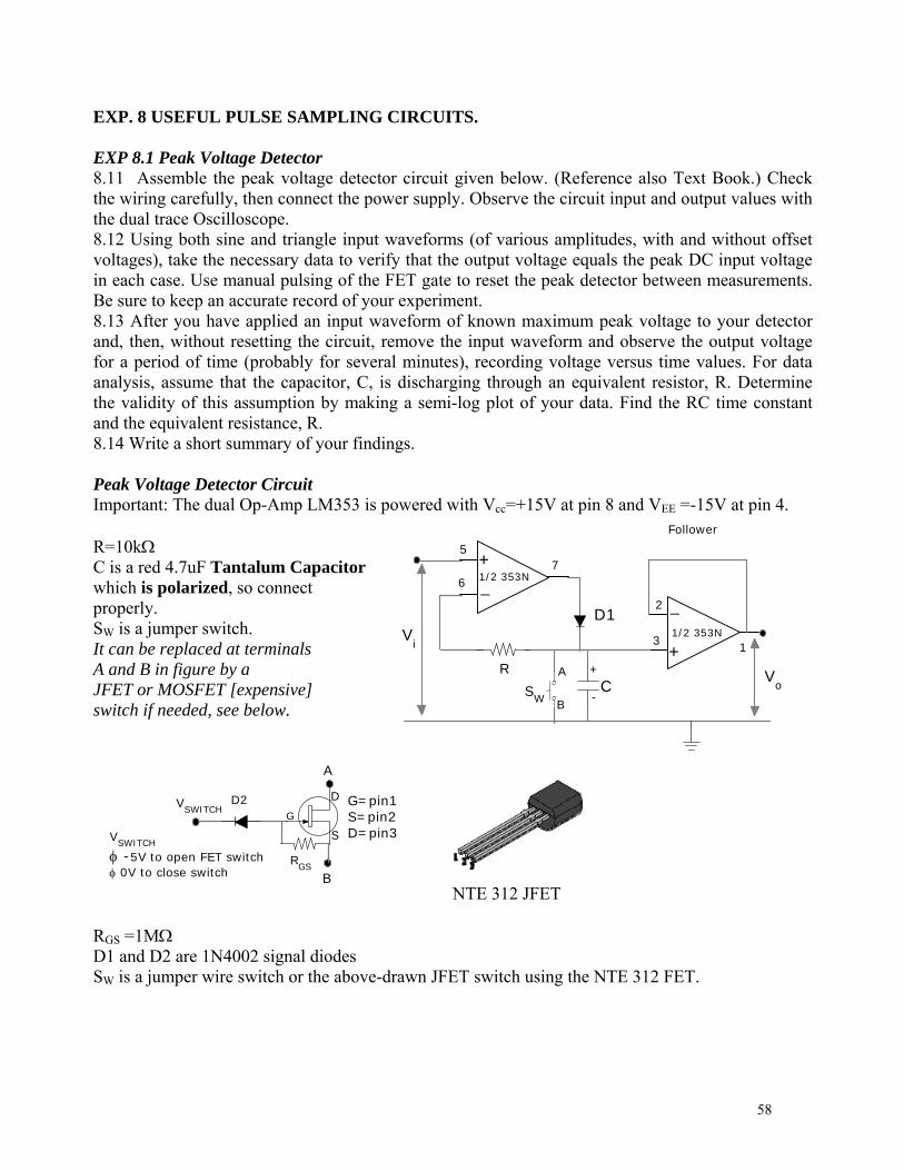
58
EXP. 8 USEFUL PULSE SAMPLING CIRCUITS. EXP 8.1 Peak Voltage Detector 8.11 Assemble the peak voltage detector circuit given below. (Reference also Text Book.) Check the wiring carefully, then connect the power supply. Observe the circuit input and output values with the dual trace Oscilloscope. 8.12 Using both sine and triangle input waveforms (of various amplitudes, with and without offset voltages), take the necessary data to verify that the output voltage equals the peak DC input voltage in each case. Use manual pulsing of the FET gate to reset the peak detector between measurements. Be sure to keep an accurate record of your experiment. 8.13 After you have applied an input waveform of known maximum peak voltage to your detector and, then, without resetting the circuit, remove the input waveform and observe the output voltage for a period of time (probably for several minutes), recording voltage versus time values. For data analysis, assume that the capacitor, C, is discharging through an equivalent resistor, R. Determine the validity of this assumption by making a semi-log plot of your data. Find the RC time constant and the equivalent resistance, R. 8.14 Write a short summary of your findings. Peak Voltage Detector Circuit Important: The dual Op-Amp LM353 is powered with Vcc=+15V at pin 8 and VEE =-15V at pin 4. R=10k C is a red 4.7uF Tantalum Capacitor which is polarized, so connect properly. SW is a jumper switch. It can be replaced at terminals A and B in figure by a JFET or MOSFET [expensive] switch if needed, see below.
NTE 312 JFET RGS =1MD1 and D2 are 1N4002 signal diodes SW is a jumper wire switch or the above-drawn JFET switch using the NTE 312 FET.
A
B
G=pin1S=pin2D=pin3
G
D
SVSWITCH
-5V to open FET switch 0V to close switch
VSWITCH
RGS
D2
LM741CN
2
13
Vo
1/2 353NVi
D1
R
SWC
+
-
1/2 353N7
6
5
Follower
A
B
+
+
__1/2 353N
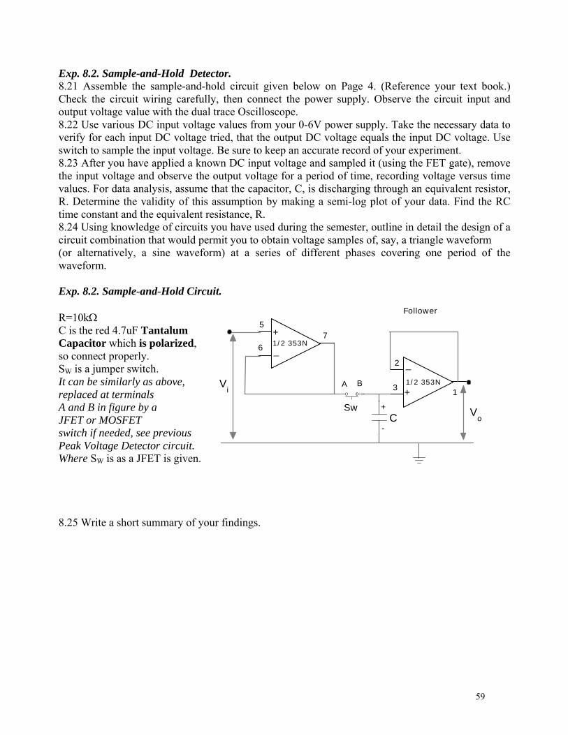
59
Exp. 8.2. Sample-and-Hold Detector. 8.21 Assemble the sample-and-hold circuit given below on Page 4. (Reference your text book.) Check the circuit wiring carefully, then connect the power supply. Observe the circuit input and output voltage value with the dual trace Oscilloscope. 8.22 Use various DC input voltage values from your 0-6V power supply. Take the necessary data to verify for each input DC voltage tried, that the output DC voltage equals the input DC voltage. Use switch to sample the input voltage. Be sure to keep an accurate record of your experiment. 8.23 After you have applied a known DC input voltage and sampled it (using the FET gate), remove the input voltage and observe the output voltage for a period of time, recording voltage versus time values. For data analysis, assume that the capacitor, C, is discharging through an equivalent resistor, R. Determine the validity of this assumption by making a semi-log plot of your data. Find the RC time constant and the equivalent resistance, R. 8.24 Using knowledge of circuits you have used during the semester, outline in detail the design of a circuit combination that would permit you to obtain voltage samples of, say, a triangle waveform (or alternatively, a sine waveform) at a series of different phases covering one period of the waveform. Exp. 8.2. Sample-and-Hold Circuit. R=10k C is the red 4.7uF Tantalum Capacitor which is polarized, so connect properly. SW is a jumper switch. It can be similarly as above, replaced at terminals A and B in figure by a JFET or MOSFET switch if needed, see previous Peak Voltage Detector circuit. Where SW is as a JFET is given. 8.25 Write a short summary of your findings.
LM741CN
2
13
Vo
1/2 353NVi
SwC
+
-
1/2 353N7
6
5
Follower
A B
+
_
+
_
1/2 353N
60
EXP. 9 DIGITAL CIRCUITS General Instructions: 1. For all experiments, do the following (details in the Appendix): 1.1 Draw the logic circuit diagrams. 1.2 Use the logic pulser for all inputs. (Exceptions may be called for in an individual experiment.) Note: An inverter (a NOT gate) placed in series with, say, the pulser QA output, converts it to QA’. 1.3 Make voltage vs. time sketches of Oscilloscope DC input traces for (a) the pulser clock, (b) all input pulse sequences used, and (c) output(s). 1.4 Give truth tables, as checked by your input/output sketches. 1.5 Answer any questions that may be asked in individual experiments. Answer all questions with complete sentences. 1.6 Write a short summary for each experiment group (6 summaries, in all). 2. For EXPS. 9.1 and 9.2, do the following: 2.1 Starting from the experimental truth table, write a Boolean expression consisting of AND statements for each Q = 1 line of the table, with all of the AND statements OR'd together. Then, use Boolean algebra identities (see your text book) to reduce this expression to simplest form. 2.2 Carry out any other Boolean algebra asked for (Karnaugh Maps). 3. EXP. 9.3 3.1 Give a detailed description of the sequential operation of each circuit. 3.2 In your summary, state the distinctive features in which the un-clocked RSFF and the clocked RSFF differ from each other. Comment on the advantages and disadvantages resulting from these differences. 4. EXPS. 9.4, 9.5, 9.6 if needed. Follow any special instructions that are given. List of Experiments and Special Instructions All diagrams for experiments, when given, will be found sequentially in the Appendix, starting on Page 1-10. If no comments or special instructions are given for any listed experiment, assume that the General Instructions given above are sufficient. NOTE WELL: Both your text and the Appendix contain important theoretical and experimental details, and precautions for carrying out digital logic experiments. Refer frequently to these sources while you are doing the experiments. Symbolism Used in the Laboratory Manual This discussion assumes positive logic, that is, Q = 1 if the logic result is true (T), and Q = 0 if the result is false (F). In terms of circuit 2-state voltages (H = high and L = low), logic-1 = H and logic-0 = L. Q = the output state resulting from any logic statement, Qn+1 = the output state that follows state, Qn, in sequence. LOGIC operations, summarized below, are defined by Truth Tables, as well as by words (see your text book):
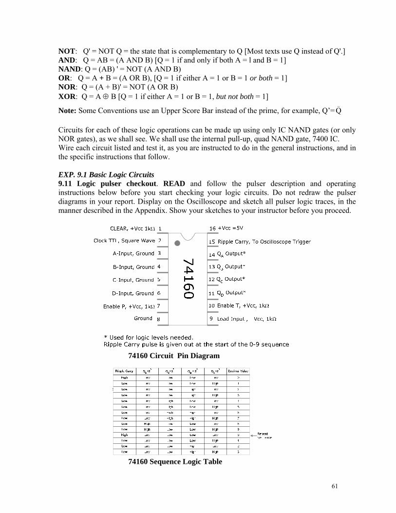
61
NOT: Q' = NOT Q = the state that is complementary to Q [Most texts use Q instead of Q'.] AND: Q = AB = (A AND B) [Q = 1 if and only if both A = l and B = 1] NAND: Q = (AB) ' = NOT (A AND B) OR: Q = A + B = (A OR B), [Q = 1 if either A = 1 or B = 1 or both = 1] NOR: Q = (A + B)' = NOT (A OR B) XOR: Q = A B [Q = 1 if either A = 1 or B = 1, but not both = 1]
Note: Some Conventions use an Upper Score Bar instead of the prime, for example, Q’=_
Q Circuits for each of these logic operations can be made up using only IC NAND gates (or only NOR gates), as we shall see. We shall use the internal pull-up, quad NAND gate, 7400 IC. Wire each circuit listed and test it, as you are instructed to do in the general instructions, and in the specific instructions that follow. EXP. 9.1 Basic Logic Circuits 9.11 Logic pulser checkout. READ and follow the pulser description and operating instructions below before you start checking your logic circuits. Do not redraw the pulser diagrams in your report. Display on the Oscilloscope and sketch all pulser logic traces, in the manner described in the Appendix. Show your sketches to your instructor before you proceed.
74160 Circuit Pin Diagram
74160 Sequence Logic Table
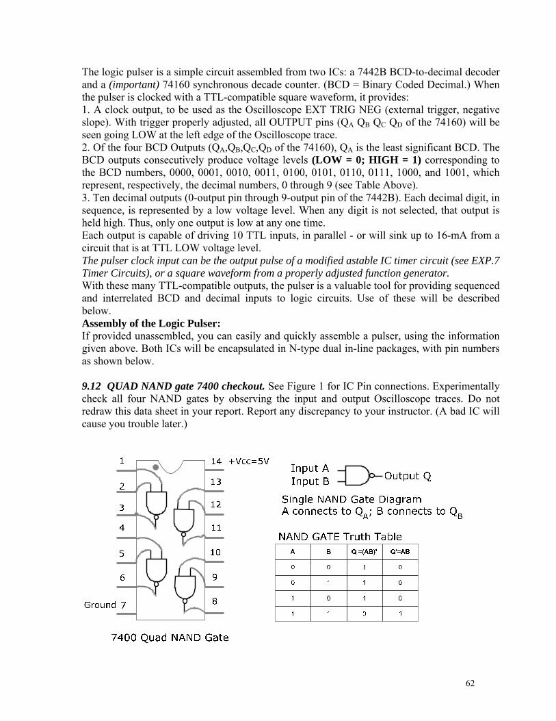
62
The logic pulser is a simple circuit assembled from two ICs: a 7442B BCD-to-decimal decoder and a (important) 74160 synchronous decade counter. (BCD = Binary Coded Decimal.) When the pulser is clocked with a TTL-compatible square waveform, it provides: 1. A clock output, to be used as the Oscilloscope EXT TRIG NEG (external trigger, negative slope). With trigger properly adjusted, all OUTPUT pins (QA QB QC QD of the 74160) will be seen going LOW at the left edge of the Oscilloscope trace. 2. Of the four BCD Outputs (QA,QB,QC,QD of the 74160), QA is the least significant BCD. The BCD outputs consecutively produce voltage levels (LOW = 0; HIGH = 1) corresponding to the BCD numbers, 0000, 0001, 0010, 0011, 0100, 0101, 0110, 0111, 1000, and 1001, which represent, respectively, the decimal numbers, 0 through 9 (see Table Above). 3. Ten decimal outputs (0-output pin through 9-output pin of the 7442B). Each decimal digit, in sequence, is represented by a low voltage level. When any digit is not selected, that output is held high. Thus, only one output is low at any one time. Each output is capable of driving 10 TTL inputs, in parallel - or will sink up to 16-mA from a circuit that is at TTL LOW voltage level. The pulser clock input can be the output pulse of a modified astable IC timer circuit (see EXP.7 Timer Circuits), or a square waveform from a properly adjusted function generator. With these many TTL-compatible outputs, the pulser is a valuable tool for providing sequenced and interrelated BCD and decimal inputs to logic circuits. Use of these will be described below. Assembly of the Logic Pulser: If provided unassembled, you can easily and quickly assemble a pulser, using the information given above. Both ICs will be encapsulated in N-type dual in-line packages, with pin numbers as shown below. 9.12 QUAD NAND gate 7400 checkout. See Figure 1 for IC Pin connections. Experimentally check all four NAND gates by observing the input and output Oscilloscope traces. Do not redraw this data sheet in your report. Report any discrepancy to your instructor. (A bad IC will cause you trouble later.)
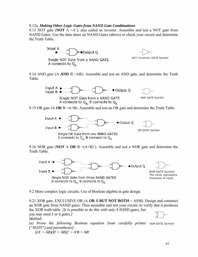
63
9.12a. Making Other Logic Gates from NAND Gate Combinations 9.13 NOT gate (NOT A =A’), also called an inverter. Assemble and test a NOT gate from NAND Gates. Use the data sheet on NAND Gates (above) to check your circuit and determine the Truth Table.
9.14 AND gate (A AND B =AB). Assemble and test an AND gate, and determine the Truth Table.
9.15 OR gate (A OR B =A+B). Assemble and test an OR gate and determine the Truth Table.
9.16 NOR gate (NOT A OR B =(A+B)’). Assemble and test a NOR gate and determine the Truth Table.
9.2 More complex logic circuits. Use of Boolean algebra in gate design. 9.21 XOR gate. EXCLUSIVE OR (A OR B BUT NOT BOTH = AB). Design and construct an XOR gate from NAND gates. Then assemble and test your circuit, to verify that it produces the XOR truth table. [It is possible to do this with only 4 NAND gates, but you may need 5 or 6 gates.] Method: (a) Prove the following Boolean equation [note carefully primes (“NOTS”) and parentheses]: [(A' + AB)(B' + AB)]' = A'B + AB'
NOT (Inverter) GATE Symbol
AND GATE Symbol
OR GATE Symbol
XOR GATE Symbol
NOR GATE SymbolThe circle representsInversion of Input
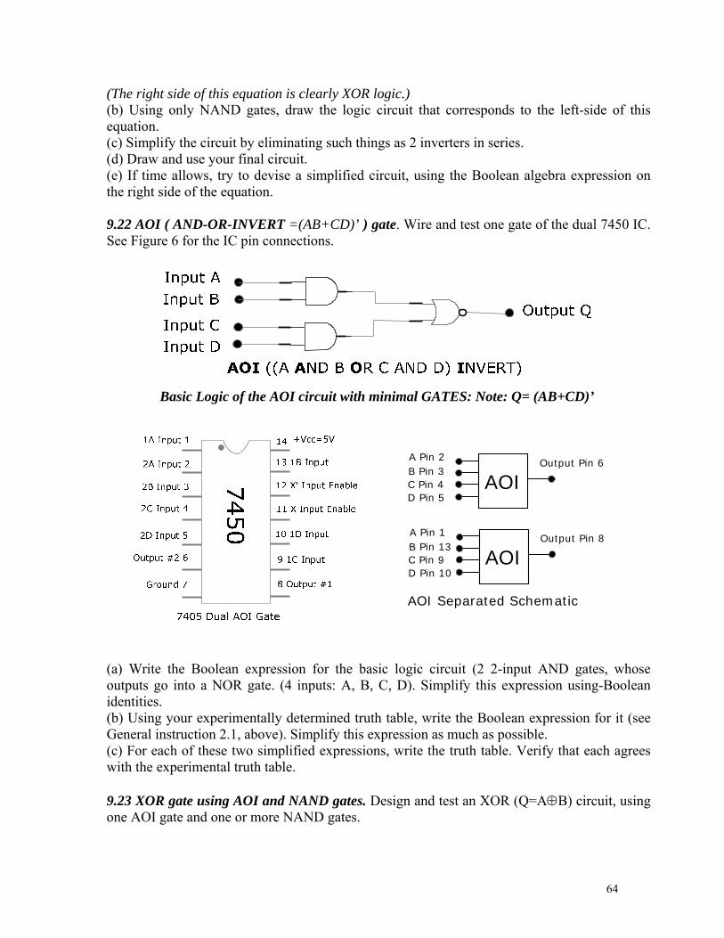
64
(The right side of this equation is clearly XOR logic.) (b) Using only NAND gates, draw the logic circuit that corresponds to the left-side of this equation. (c) Simplify the circuit by eliminating such things as 2 inverters in series. (d) Draw and use your final circuit. (e) If time allows, try to devise a simplified circuit, using the Boolean algebra expression on the right side of the equation. 9.22 AOI ( AND-OR-INVERT =(AB+CD)’ ) gate. Wire and test one gate of the dual 7450 IC. See Figure 6 for the IC pin connections.
Basic Logic of the AOI circuit with minimal GATES: Note: Q= (AB+CD)’
(a) Write the Boolean expression for the basic logic circuit (2 2-input AND gates, whose outputs go into a NOR gate. (4 inputs: A, B, C, D). Simplify this expression using-Boolean identities. (b) Using your experimentally determined truth table, write the Boolean expression for it (see General instruction 2.1, above). Simplify this expression as much as possible. (c) For each of these two simplified expressions, write the truth table. Verify that each agrees with the experimental truth table. 9.23 XOR gate using AOI and NAND gates. Design and test an XOR (Q=AB) circuit, using one AOI gate and one or more NAND gates.
AOIA Pin 2B Pin 3C Pin 4D Pin 5
Output Pin 6
AOIA Pin 1B Pin 13C Pin 9D Pin 10
Output Pin 8
AOI Separated Schematic
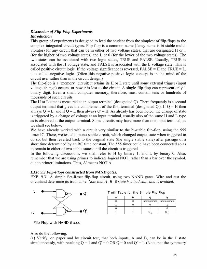
65
Discussion of Flip-Flop Experiments Introduction This group of experiments is designed to lead the student from the simplest of flip-flops to the complex integrated circuit types. Flip-flop is a common name (fancy name is bi-stable multi-vibrator) for any circuit that can be in either of two voltage states, that are designated H or 1 (for the higher of two voltage states) and L or 0 (for the lower of the two voltage states). The two states can be associated with two logic states, TRUE and FALSE. Usually, TRUE is associated with the H voltage state, and FALSE is associated with the L voltage state. This is called positive circuit logic. If the voltage significance is reversed, FALSE = H and TRUE = L, it is called negative logic. (Often this negative-positive logic concept is in the mind of the circuit user rather than in the circuit design.) The flip-flop is a "memory" circuit; it retains its H or L state until some external trigger (input voltage change) occurs, or power is lost to the circuit. A single flip-flop can represent only 1 binary digit. Even a small computer memory, therefore, must contain tens or hundreds of thousands of such circuits. The H or L state is measured at an output terminal (designated Q). There frequently is a second output terminal that gives the complement of the first terminal (designated Q'). If Q = H then always Q' = L, and if Q = L then always Q' = H. As already has been noted, the change of state is triggered by a change of voltage at an input terminal, usually also of the same H and L type as is observed at the output terminal. Some circuits may have more than one input terminal, as we shall see below. We have already worked with a circuit very similar to the bi-stable flip-flop, using the 555 timer IC. There, we tested a mono-stable circuit, which changed output state when triggered to do so, but then reverted back to the original state (the single stable state) after passage of a short time determined by an RC time constant. The 555 timer could have been connected so as to remain in either of two stable states until the circuit is triggered. In the following discussions, we shall refer to H by binary 1, and L by binary 0. Also, remember that we are using primes to indicate logical NOT, rather than a bar over the symbol, due to printer limitations. Thus, A' means NOT A. EXP. 9.3 Flip-Flops constructed from NAND gates. EXP. 9.31 A simple Set-Reset flip-flop circuit, using two NAND gates. Wire and test the circuitand determine its truth table. Note that A=B=0 state is a bad state and is avoided.
Also do the following: (a) Verify, on paper and by circuit test, that both inputs, A and B, can be in the 1 state simultaneously, with resulting Q = 1 and Q' = 0 OR Q = 0 and Q' = 1. (Note that the symmetry
A B Q Q'
0 0 Indeterminate Indeterminate
1 0 0 1
0 1 1 0
1 1 Q-1
Q-1
'
Truth Table for the Simple Flip Flop
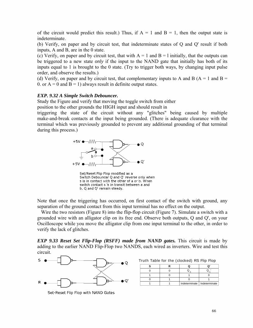
66
of the circuit would predict this result.) Thus, if A = 1 and B = 1, then the output state is indeterminate. (b) Verify, on paper and by circuit test, that indeterminate states of Q and Q' result if both inputs, A and B, are in the 0 state. (c) Verify, on paper and by circuit test, that with A = 1 and B = l initially, that the outputs can be triggered to a new state only if the input to the NAND gate that initially has both of its inputs equal to 1 is brought to the 0 state. (Try to trigger both ways, by changing input pulse order, and observe the results.) (d) Verify, on paper and by circuit test, that complementary inputs to A and B (A = 1 and B = 0. or A = 0 and B = 1) always result in definite output states. EXP. 9.32 A Simple Switch Debouncer. Study the Figure and verify that moving the toggle switch from either position to the other grounds the HIGH input and should result in triggering the state of the circuit without any "glitches" being caused by multiple make-and-break contacts at the input being grounded. (There is adequate clearance with the terminal which was previously grounded to prevent any additional grounding of that terminal during this process.)
Note that once the triggering has occurred, on first contact of the switch with ground, any separation of the ground contact from this input terminal has no effect on the output. Wire the two resistors (Figure 8) into the flip-flop circuit (Figure 7). Simulate a switch with a grounded wire with an alligator clip on its free end. Observe both outputs, Q and Q', on your Oscilloscope while you move the alligator clip from one input terminal to the other, in order to verify the lack of glitches. EXP 9.33 Reset Set Flip-Flop (RSFF) made from NAND gates. This circuit is made by adding to the earlier NAND Flip-Flop two NANDS, each wired as inverters. Wire and test this circuit.
S R Q Q'
0 0 Q-1
Q-1
'
1 0 1 0
0 1 0 1
1 1 Indeterminate Indeterminate
Truth Table for the (clocked) RS Flip Flop
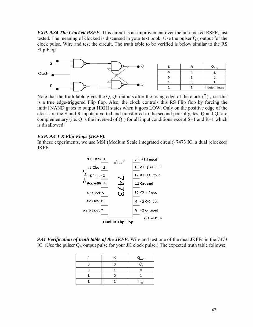
67
EXP. 9.34 The Clocked RSFF. This circuit is an improvement over the un-clocked RSFF, just tested. The meaning of clocked is discussed in your text book. Use the pulser QA output for the clock pulse. Wire and test the circuit. The truth table to be verified is below similar to the RS Flip Flop.
Note that the truth table gives the Q, Q’ outputs after the rising edge of the clock () , i.e. this is a true edge-triggered Flip flop. Also, the clock controls this RS Flip flop by forcing the initial NAND gates to output HIGH states when it goes LOW. Only on the positive edge of the clock are the S and R inputs inverted and transferred to the second pair of gates. Q and Q’ are complementary (i.e. Q is the inversed of Q’) for all input conditions except S=1 and R=1 which is disallowed. EXP. 9.4 J-K Flip-Flops (JKFF). In these experiments, we use MSI (Medium Scale integrated circuit) 7473 IC, a dual (clocked) JKFF.
9.41 Verification of truth table of the JKFF. Wire and test one of the dual JKFFs in the 7473 IC. (Use the pulser QA output pulse for your JK clock pulse.) The expected truth table follows:
S R Qn+1
0 0 Qn
0 1 0
1 0 1
1 1 Indeterminate
J K Qn+1
0 0 Qn
0 1 0
1 0 1
1 1 Qn'
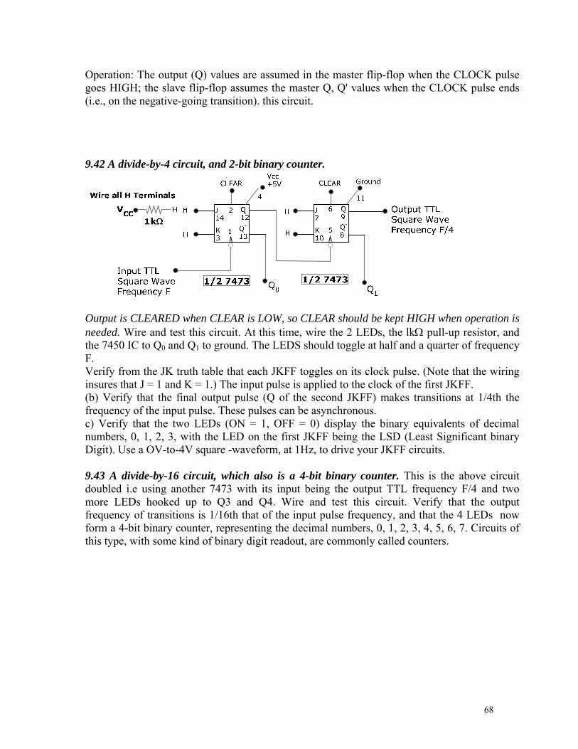
68
Operation: The output (Q) values are assumed in the master flip-flop when the CLOCK pulse goes HIGH; the slave flip-flop assumes the master Q, Q' values when the CLOCK pulse ends (i.e., on the negative-going transition). this circuit. 9.42 A divide-by-4 circuit, and 2-bit binary counter.
Output is CLEARED when CLEAR is LOW, so CLEAR should be kept HIGH when operation is needed. Wire and test this circuit. At this time, wire the 2 LEDs, the lk pull-up resistor, and the 7450 IC to Q0 and Q1 to ground. The LEDS should toggle at half and a quarter of frequency F. Verify from the JK truth table that each JKFF toggles on its clock pulse. (Note that the wiring insures that J = 1 and K = 1.) The input pulse is applied to the clock of the first JKFF. (b) Verify that the final output pulse (Q of the second JKFF) makes transitions at 1/4th the frequency of the input pulse. These pulses can be asynchronous. c) Verify that the two LEDs (ON = 1, OFF = 0) display the binary equivalents of decimal numbers, 0, 1, 2, 3, with the LED on the first JKFF being the LSD (Least Significant binary Digit). Use a OV-to-4V square -waveform, at 1Hz, to drive your JKFF circuits. 9.43 A divide-by-16 circuit, which also is a 4-bit binary counter. This is the above circuit doubled i.e using another 7473 with its input being the output TTL frequency F/4 and two more LEDs hooked up to Q3 and Q4. Wire and test this circuit. Verify that the output frequency of transitions is 1/16th that of the input pulse frequency, and that the 4 LEDs now form a 4-bit binary counter, representing the decimal numbers, 0, 1, 2, 3, 4, 5, 6, 7. Circuits of this type, with some kind of binary digit readout, are commonly called counters.
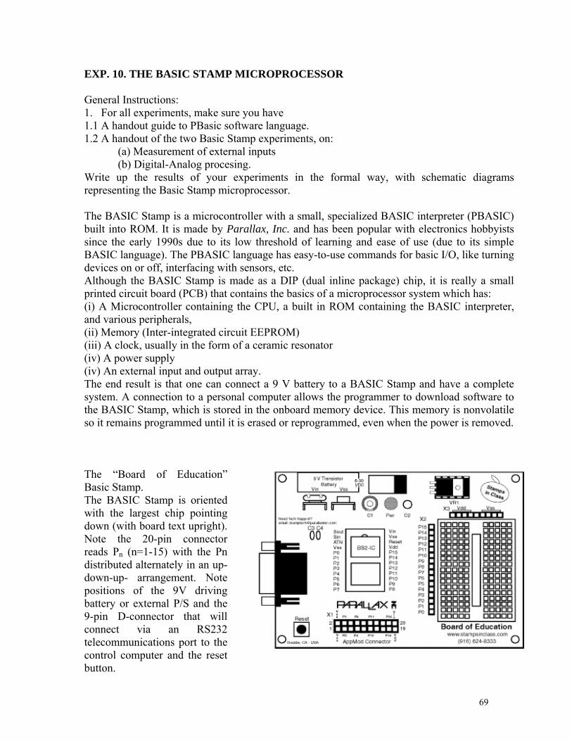
69
EXP. 10. THE BASIC STAMP MICROPROCESSOR General Instructions: 1. For all experiments, make sure you have 1.1 A handout guide to PBasic software language. 1.2 A handout of the two Basic Stamp experiments, on: (a) Measurement of external inputs (b) Digital-Analog procesing. Write up the results of your experiments in the formal way, with schematic diagrams representing the Basic Stamp microprocessor. The BASIC Stamp is a microcontroller with a small, specialized BASIC interpreter (PBASIC) built into ROM. It is made by Parallax, Inc. and has been popular with electronics hobbyists since the early 1990s due to its low threshold of learning and ease of use (due to its simple BASIC language). The PBASIC language has easy-to-use commands for basic I/O, like turning devices on or off, interfacing with sensors, etc. Although the BASIC Stamp is made as a DIP (dual inline package) chip, it is really a small printed circuit board (PCB) that contains the basics of a microprocessor system which has: (i) A Microcontroller containing the CPU, a built in ROM containing the BASIC interpreter, and various peripherals, (ii) Memory (Inter-integrated circuit EEPROM) (iii) A clock, usually in the form of a ceramic resonator (iv) A power supply (iv) An external input and output array. The end result is that one can connect a 9 V battery to a BASIC Stamp and have a complete system. A connection to a personal computer allows the programmer to download software to the BASIC Stamp, which is stored in the onboard memory device. This memory is nonvolatile so it remains programmed until it is erased or reprogrammed, even when the power is removed. The “Board of Education” Basic Stamp. The BASIC Stamp is oriented with the largest chip pointing down (with board text upright). Note the 20-pin connector reads Pn (n=1-15) with the Pn distributed alternately in an up-down-up- arrangement. Note positions of the 9V driving battery or external P/S and the 9-pin D-connector that will connect via an RS232 telecommunications port to the control computer and the reset button.
70
APPENDIX 1. PBASIC Quick Reference Guide
BRANCHING IF...THEN IF condition THEN addressLabel Evaluate condition and, if true, go to the point in the program marked by addressLabel. · Condition is a statement, such as “x=7” that can be evaluated as true of false. · AddressLabel is a label that specifies where to go in the event that the condition is true. BRANCH BRANCH offset, [address0, address1, …address N] Go to the address specified by offset (if in range). · Offset is a variable / constant that specifies which of the listed address to go to (0-N). · Addresses are labels that specify where to go. GOTO GOTO addressLabel Go to the point in the program specified by addressLabel. · AddressLabel is a label that specifies where to go. GOSUB GOSUB addressLabel Store the address of the next instruction after GOSUB, then go to the point in the program specified by addressLabel. · AddressLabel is a label that specifies where to go. RETURN Return from subroutine – sends the program back to the address (instruction) immediately following the most recent GOSUB. Page 98 • “What’s a Microcontroller?” Student Guide Version 1.5
LOOPING FOR...NEXT FOR variable = start to end {stepVal} …NEXT Create a repeating loop that executes the program lines between FOR and NEXT, incrementing or decrementing variable according to stepVal until the value of the variable pases the end value. · Variable is a bit, nib, byte, or word variable used as a counter. · Start is a variable or constant that specifies the initial value of the variable. · End is a variable or constant that specifies the end value of the variable. When the value of the variable passes end, the FOR . . . NEXT loop stops executing and the program goes on to the instruction after NEXT. · StepVal is an optional variable or constant by which the variable increases or decreases with each trip through the FOR / NEXT loop. If start is larger than end, PBASIC2 understands stepVal to be negative, even though no minus sign is used.
71
NUMERICS LOOKUP LOOKUP index, [value0, value1,... valueN], variable Look up the value specified by the index and store it in a variable. If the index exceeds the highest index value of the items in the list, variable is unaffected. A maximum of 256 values can be included in the list. · index is a constant, expression or a bit, nibble, byte or word variable. · value0, value1, etc. are constants, expressions or bit, nibble, byte or word variables. · variable is a bit, nibble, byte or word variable. LOOKDOWN LOOKDOWN value, {??,} [value0, value1,... valueN], variable · value is a constant, expression or a bit, nibble, byte or word variable. · ?? is =, <>, >, <, <=, =>. (= is the default). · value0, value1, etc. are constants, expressions or bit, nibble, byte or word variables. · variable is a bit, nibble, byte or word variable. RANDOM RANDOM variable Generate a pseudo-random number. · variable is a byte or word variable in the range 0..65535.
DIGITAL I/O INPUT INPUT pin Make the specified pin an input (write a 0 to the corresponding bit of DIRS). · pin is a constant, expression or a bit, nibble, byte or word variable in the range 0..15. OUTPUT OUTPUT pin Make the specified pin an output (write a 1 to the corresponding bit of DIRS). · pin is a constant, expression or a bit, nibble, byte or word variable in the range 0..15. REVERSE REVERSE pin If pin is an output, make it an input. If pin is an input, make it an output. · pin is a constant, expression or a bit, nibble, byte or word variable in the range 0..15. LOW LOW pin Make pin output low (write 1 to the corresponding bit of DIRS and 0 to the corresponding bit of OUTS). · pin is a constant, expression or a bit, nibble, byte or word variable in the range 0..15.
72
HIGH HIGH pin Make the specified pin output high (write 1s to the corresponding bits of both DIRS and OUTS). · pin is a constant, expression or a bit, nibble, byte or word variable in the range 0..15. TOGGLE TOGGLE pin Invert the state of a pin. · pin is a constant, expression or a bit, nibble, byte or word variable in the range 0..15. Appendix B: PBASIC Quick Reference Guide Page 100 • “What’s a Microcontroller?” Student Guide Version 1.5 PULSIN PULSIN pin, state, variable Measure an input pulse (resolution of 2 µs). · pin is a constant, expression or a bit, nibble, byte or word variable in the range 0..15. · state is a constant, expression or a bit, nibble, byte or word variable in the range 0..1. · variable is a bit, nibble, byte or word variable. Measurements are in 2uS intervals and the instruction will time out in 0.13107 seconds. PULSOUT PULSOUT pin, period Output a timed pulse by inverting a pin for some time (resolution of 2 µs). · pin is a constant, expression or a bit, nibble, byte or word variable in the range 0..15. · period is a constant, expression or a bit, nibble, byte or word · variable in the range 0..65535 representing the pulse width in 2uS units. BUTTON BUTTON pin, downstate, delay, rate, workspace, targetstate, label Debounce button, perform auto-repeat, and branch to address if button is in target state. · pin is a constant, expression or a bit, nibble, byte or word variable in the range 0..15. · downstate is a constant, expression or a bit, nibble, byte or word variable in the range 0..1. · delay is a constant, expression or a bit, nibble, byte or word variable in the range 0..255. · rate is a constant, expression or a bit, nibble, byte or word variable in the range 0..255. · workspace is a byte or word variable. · targetstate is a constant, expression or a bit, nibble, byte or word variable in the range 0..1. · label is a valid label to jump to in the event of a button press. SHIFTIN SHIFTIN dpin, cpin, mode, [result{\bits} { ,result{\bits}... }] Shift bits in from parallel-to-serial shift register. · dpin is a constant, expression or a bit, nibble, byte or word variable in the range 0..15 specifying the data pin. · cpin is a constant, expression or a bit, nibble, byte or word variable in the range 0..15 specifying the clock pin.
73
· mode is a constant, symbol, expression or a bit, nibble, byte or word variable in the range 0..4 specifying the bit order and clock mode. 0 or MSBPRE = msb first, pre-clock, 1 or LSBPRE = lsb first, pre-clock, 2 or MSBPOST = msb first, post-clock, 3 or LSBPOST = lsb first, post-clock. · result is a bit, nibble, byte or word variable where the received data is stored. · bits is a constant, expression or a bit, nibble, byte or word variable in the range 1..16 specifying the number of bits to receive in result. The default is 8. SHIFTOUT SHIFTOUT dpin, cpin, mode, [data{\bits} {, data{\bits}... }] Shift bits out to serial-to-parallel shift register. · dpin is a constant, expression or a bit, nibble, byte or word variable in the range 0..15 specifying the data pin. · cpin is a constant, expression or a bit, nibble, byte or word variable in the range 0..15 specifying the clock pin. · mode is a constant, symbol, expression or a bit, nibble, byte or word variable in the range 0..1 specifying the bit order. 0 or LSBFIRST = lsb first, 1 or MSBFIRST = msb first. · data is a constant, expression or a bit, nibble, byte or word variable containing the data to send out. · bits is a constant, expression or a bit, nibble, byte or word variable in the range 1..16 specifying the number of bits of data to send. The default is 8. COUNT COUNT pin, period, result Count cycles on a pin for a given amount of time (0 - 125 kHz, assuming a 50/50 duty cycle). · pin is a constant, expression or a bit, nibble, byte or word variable in the range 0..15. · period is a constant, expression or a bit, nibble, byte or word variable in the range 0..65535. · result is a bit, nibble, byte or word variable. XOUT XOUT mpin, zpin, [house\keyorcommand{\cycles} {, house\keyorcommand{\cycles}... }] Generate X-10 powerline control codes. For use with TW523 or TW513 powerline interface module. · mpin is a constant, expression or a bit, nibble, byte or word variable in the range 0..15 specifying the modulation pin. · zpin is a constant, expression or a bit, nibble, byte or word variable in the range 0..15 specifying the zerocrossing pin. · house is a constant, expression or a bit, nibble, byte or word variable in the range 0..15 specifying the house code A..P respectively. · keycommand is a constant, expression or a bit, nibble, byte or word variable in the range 0..15 specifying keys 1..16 respectively or is one of the commands shown for X-10 light control in the BASIC Stamp Manual Version 1.9. These commands include lights on, off, dim and bright. · cycles is a constant, expression or a bit, nibble, byte or word variable in the range 2..65535 specifying the number of cycles to send. (Default is 2).
74
SERIAL I/O
SERIN SERIN rpin{\fpin}, baudmode, {plabel,} {timeout, tlabel,} [inputdata] Serial input with optional qualifiers, time-out, and flow control. If qualifiers are given, then the instruction will wait until they are received before filling variables or continuing to the next instruction. If a time-out value is given, then the instruction will abort after receiving nothing for a given amount of time. Baud rates of 300 - 50,000 are possible (0 - 19,200 with flow control). Data received must be N81 (no parity, 8 data bits, 1 stop bit) or E71 (even parity, 7 data bits, 1 stop bit). · rpin is a constant, expression or a bit, nibble, byte or word variable in the range 0..16. · fpin is a constant, expression or a bit, nibble, byte or word variable in the range 0..15. · baudmode is a constant, expression or a bit, nibble, byte or word variable in the range 0..65535. · plabel is a label to jump to in case of a parity error. · timeout is a constant, expression or a bit, nibble, byte or word variable in the range 0..65535 representing the number of milliseconds to wait for an incoming message. · tlabel is a label to jump to in case of a timeout. · inputdata is a set of constants, expressions and variable names separated by commas and optionally proceeded by the formatters available in the DEBUG command, except the ASC and REP formatters. Additionally, the following formatters are available: 1. STR bytearray\L{\E} input a string into bytearray of length L with optional end-character of E. (0’s will fill remaining bytes). 2. SKIP L input and ignore L bytes. 3. WAITSTR bytearray{\L} Wait for bytearray string (ofL length, or terminated by 0 if parameter is not specified and is 6 bytes maximum). 4. WAIT (value {,value...}) Wait for up to a six-byte se-quence. SEROUT SEROUT tpin{\fpin}, baudmode, {pace,} {timeout, tlabel,} [outputdata] Send data serially with optional byte pacing and flow control. If a pace value is given, then the instruction will insert a specified delay between each byte sent (pacing is not available with flow control). Baud rates of 300 - 50,000 are possible (0 - 19,200 with flow control). Data is sent as N81 (no parity, 8 data bits, 1 stop bit) or E71 (even parity, 7 data bits, 1 stop bit). · tpin is a constant, expression or a bit, nibble, byte or word variable in the range 0..16. · fpin is a constant, expression or a bit, nibble, byte or word variable in the range 0..15. · baudmode is a constant, expression or a bit, nibble, byte or word variable in the range 0..60657. · pace is a constant, expression or a bit, nibble, byte or word variable in the range 0..65535 specifying a time (in milliseconds) to delay between transmitted bytes. This value can only be specified if the fpin is not specified. · timeout is a constant, expression or a bit, nibble, byte or word variable in the range 0..65535
75
representing the number of milliseconds to wait for the signal to transmit the message. This value can only be specified if the fpin is specified. · tlabel is a label to jump to in case of a timeout. This can only be specified if the fpin is specified. · outputdata is a set of constants, expressions and variable names separated by commas and optionally proceeded by the formatters available in the DEBUG command.
ANALOG I/O
PWM PWM pin, duty, cycles Output PWM, then return pin to input. This can be used to output analog voltages (0-5V) using a capacitor and resistor. · pin is a constant, expression or a bit, nibble, byte or word variable in the range 0..15. · duty is a constant, expression or a bit, nibble, byte or word variable in the range 0..255. · cycles is a constant, expression or a bit, nibble, byte or word variable in the range 0..255 representing the number of 1ms cycles to output. RCTIME RCTIME pin, state, variable Measure an RC charge/discharge time. Can be used to measure potentiometers. · pin is a constant, expression or a bit, nibble, byte or word variable in the range 0..15. · state is a constant, expression or a bit, nibble, byte or word variable in the range 0..1. · variable is a bit, nibble, byte or word variable.
SOUND
FREQOUT FREQOUT pin, milliseconds, freq1 {,freq2} Generate one or two sinewaves of specified frequencies (each from 0 - 32767 hz.). · pin is a constant, expression or a bit, nibble, byte or word variable in the range of 0..15. · milliseconds is a constant, expression or a bit, nibble, byte or word variable. · freq1 and freq2 are constant, expression or bit, nibble, byte or word variables in the range 0..32767 representing the correspond-ing frequencies. DTMFOUT DTMFOUT pin, {ontime, offtime,}[key{,key...}] Generate DTMF telephone tones. · pin is a constant, expression or a bit, nibble, byte or word variable in the range 0..15. · ontime and offtime are constants, expressions or bit, nibble, byte or word variables in the range 0..65535. · key is a constant, expression or a bit, nibble, byte or word variable in the range 0..15.
EEPROM ACCESS
DATA DATA {pointer} DATA {@location,} {WORD} {data}{(size)} {, { WORD} {data}{(size)}...} Store data in EEPROM before downloading PBASIC program. · pointer is an optional undefined constant name or a bit, nibble, byte or word variable which is assigned the value of the first memory location in which data is written.
76
· location is an optional constant, expression or a bit, nibble, byte or word variable which designates the first memory location in which data is to be written. · word is an optional switch which causes DATA to be stored as two separate bytes in memory. · data is an optional constant or expression to be written to memory. · size is an optional constant or expression which designates the number of bytes of defined or undefined data to write/reserve in memory. If DATA is not specified then undefined data space is reserved and if DATA is specified then SIZE bytes of data equal to DATA are written to memory. READ READ location, variable Read EEPROM byte into variable. · location is a constant, expression or a bit, nibble, byte or word variable in the range 0..2047. · variable is a bit, nibble, byte or word variable. WRITE WRITE location, data Write byte into EEPROM. · location is a constant, expression or a bit, nibble, byte or word variable in the range 0..2047. · data is a constant, expression or a bit, nibble, byte or word variable. TIME PAUSE PAUSE milliseconds Pause execution for 0–65535 milliseconds. · milliseconds is a constant, expression or a bit, nibble, byte or word variable in the range 0..65535.
POWER CONTROL NAP NAP period Nap for a short period. Power consumption is reduced to 50 uA (assuming no loads). · period is a constant, expression or a bit, nibble, byte or word variable in the range 0..7 representing 18ms intervals. SLEEP SLEEP seconds Sleep for 1-65535 seconds. Power consumption is reduced to approximately 50 µA. · seconds is a constant, expression or a bit, nibble, byte or word variable in the range 0..65535 specifying the number of seconds to sleep. END END · Sleep until the power cycles or the PC connects. Power consumption is reduced to approximately 50 µA.
PROGRAM DEBUGGING DEBUG DEBUG outputdata{,outputdata...} Send variables to PC for viewing.

77
· outputdata is a text string, constant or a bit, nibble, byte or word variable. If no formatters are specified DEBUG defaults to ASCII character display without spaces or carriage returns following the value.