Embed Size (px)
Citation preview

Third Year Computer Engineering Electrical Dept.
1
Introduction to Computer Architecture
Organization and Architecture Computer Architecture refers to those attributes of a system that have a direct impact on the logical execution of a program. Examples:
• the instruction set • the number of bits used to represent various data types • I/O mechanisms • memory addressing techniques
Computer Organization refers to the operational units and their interconnections that realize the architectural specifications. Examples are things that are transparent to the programmer:
• control signals • interfaces between computer and peripherals • the memory technology being used
Structure and Function Modem computers contain millions of electronic components The key to describing such systems is to recognize their hierarchical nature
• They are a set of layers or levels of interrelated subsystems • Each level consists of a set of components and their inter-relationships
The behavior of each level depends only on a simplified, abstracted characterization of the system at the next lower level At each level, the designer is concerned with:
• Structure: The way in which the components are interrelated • Function: The operation of each individual component as part of the
Structure.
BASIC COMPUTER COMPONENTS Basic Computer Components are:
• Input devices (sends data to the CPU) • Secondary Storage Devices (stores programs and data) • Central Processing Unit (CPU) (execute instructions) • Output Devices (shows us information )
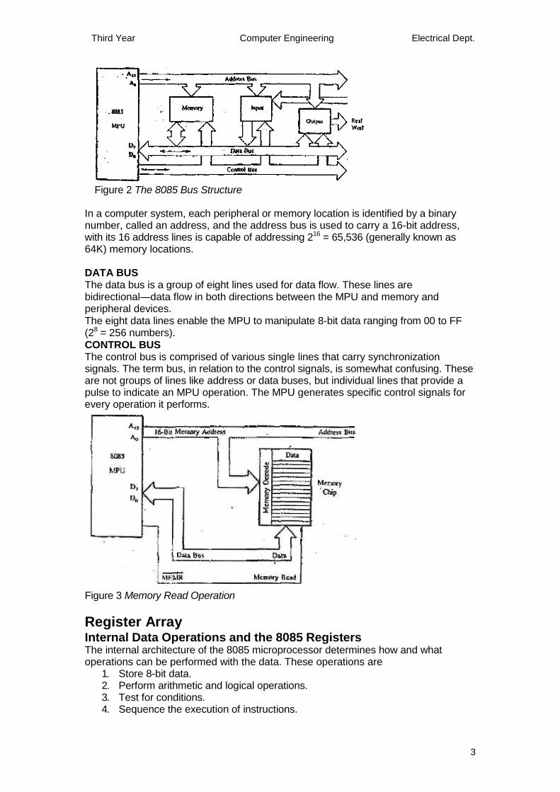
Organization of a Microprocessor-Based System Figure 1 shows a simplified but formal structure of a microprocessor-based system. It includes three components: microprocessor, I/O (input/output), and memory (read/write memory and read-only memory). These components are organized around a common communication path called a bus. The entire group of components is also referred to as a system or a microcomputer system. It is necessary to differentiate between the terms microprocessor and microcomputer. The microprocessor is one component of the microcomputer. On the other hand, the microcomputer is a complete computer, except that CPU functions of the microcomputer are performed by the microprocessor. Similarly, the term peripheral is used for input/output devices.

Third Year Computer Engineering Electrical Dept.
2
Figure 1 Microprocessor-Based System with Bus Architecture
MICROPROCESSOR The microprocessor is capable of performing various computing functions and making decisions to change the sequence of program execution. In large computers, a CPU implemented on one or more circuit boards performs these computing functions. The microprocessor is in many ways similar to the CPU, but includes all the logic circuitry, including the control unit, on one chip. The microprocessor can be divided into three segments, as shown in Figure 1: arithmetic/logic unit (ALU), register array, and control unit. Arithmetic/Logic Unit This is the area of the microprocessor where various computing functions are performed on data. The ALU unit performs such arithmetic operations as addition and subtraction, and such logic operations as AND, OR, and NOT. SYSTEM BUS The system bus is a communication path between the microprocessor and peripherals; it is nothing but a group of wires to carry bits. All peripherals (and memory) share the same bus; however, the microprocessor communicates with only one peripheral at a time. The timing is provided by the control unit of the microprocessor.
8085 Bus Organization The MPU performs primarily four operations:
1. Memory Read: Reads data (or instructions) from memory. 2. Memory Write: Writes data (or instructions) into memory. 3. I/O Read: Accepts data from input devices. 4. I/O Write: Sends data to output devices.
To communicate with a peripheral (or a memory location), the MPU needs to perform the following steps:
• Step 1: Identify the peripheral or the memory location (with its address). • Step 2: Transfer data. • Step 3: Provide timing or synchronization signals.
The 8085 MPU performs these functions using three sets of communication lines called buses: the address bus, the data bus, and the control bus (Figure 2). ADDRESS BUS The address bus is a group of 16 lines generally identified as A0 to A15. The address bus is unidirectional: bits follow in one direction—from the MPU to peripheral devices The MPU uses the address bus to perform the first function: identifying a peripheral or a memory location (Step 1).
Third Year Computer Engineering Electrical Dept.
3
Figure 2 The 8085 Bus Structure
In a computer system, each peripheral or memory location is identified by a binary number, called an address, and the address bus is used to carry a 16-bit address, with its 16 address lines is capable of addressing 216 = 65,536 (generally known as 64K) memory locations.
DATA BUS The data bus is a group of eight lines used for data flow. These lines are bidirectional—data flow in both directions between the MPU and memory and peripheral devices. The eight data lines enable the MPU to manipulate 8-bit data ranging from 00 to FF (28 = 256 numbers). CONTROL BUS The control bus is comprised of various single lines that carry synchronization signals. The term bus, in relation to the control signals, is somewhat confusing. These are not groups of lines like address or data buses, but individual lines that provide a pulse to indicate an MPU operation. The MPU generates specific control signals for every operation it performs.
Figure 3 Memory Read Operation
Register Array Internal Data Operations and the 8085 Registers The internal architecture of the 8085 microprocessor determines how and what operations can be performed with the data. These operations are
1. Store 8-bit data. 2. Perform arithmetic and logical operations. 3. Test for conditions. 4. Sequence the execution of instructions.

Third Year Computer Engineering Electrical Dept.
4
5. Store data temporarily during execution in the defined R/W memory locations called the stack.
Figure 4 The 8085 Programmable Registers
REGISTERS The 8085 has six general-purpose registers. These registers are identified as B, C, D, E, H, and L, as shown in Figure 4. They can be combined as register pairs— BC, DE, and HL—to perform some 16-bit operations. These registers are programmable, meaning that a programmer can use them to load or transfer data from the registers by using instructions. Conceptually, the registers can be viewed as memory locations, except they are built inside the microprocessor and identified by specific letters. Some microprocessors do not have these types of registers; instead, they use memory space as their registers.
ACCUMULATOR The accumulator is an 8-bit register that is part of the arithmetic/logic unit (ALU). This register is used to store 8-bit data and in-performing arithmetic and logical operations. The result of an operation is stored in the accumulator. The accumulator is also identified as register A.
FLAGS The ALU includes five flip-flops that are set or reset according to data conditions in the accumulator and other registers. For example, after an addition of two numbers, if the sum in the accumulator is larger than eight bits, the flip-flop that is used to indicate a carry, called the Carry (CY) flag, is set to one. When an arithmetic operation results in zero, the flip-flop called the Zero (Z) flag is set to one. The 8085 has five flags to indicate five different types of data conditions. They are Zero (Z), Carry (CY), Sign (S), Parity (P), and Auxiliary Carry (AC) flags. The most commonly used flags arc Sign, Zero, and Carry. These flags have critical importance in the decision-making process of the microprocessor. The conditions (set or reset) of the flags are tested through software instructions. The combination of Accumulator and Flag is called Program Status Word PSW. The detailed Flag register is shown below
PROGRAM COUNTER (PC) This register is a memory pointer. Memory locations have 16-bit addresses, and

Third Year Computer Engineering Electrical Dept.
5
that is why this is a 16-bit The microprocessor uses this register to sequence the execution of instructions. The function of the program counter is to point to the memory address from which the next byte is to be fetched. When a byte (machine code) is being fetched, the program counter is incremented by one to point to the next memory location. STACK POINTER (SP) The stack pointer is also a 16-bit register used as a memory pointer; initially, it will be called the stack pointer register to emphasize that it is a register. It points to a memory location in R/W memory, called the stack. The beginning of the stack is defined by loading a 16-bit address in the stack pointer (register). I/O (INPUT/OUTPUT) The other component of a microprocessor-based system is I/O (input/output); it communicates with the outside world. I/O includes two types of devices: input and output; these I/O devices are also known as peripherals. The input devices such as a keyboard, switches … The output devices transfer data from the microprocessor to the outside world. They include devices such as light emitting diodes (LEDs), a cathode-ray-tube (CRT)… External devices (or signals) can initiate the following operations, for which individual pins on the microprocessor chip are assigned: • Reset: When the reset is activated, all internal operations are suspended and the
program counter is cleared (it holds 0000H). Now the program execution can again begin at the zero memory address
• Interrupt: The microprocessor can be interrupted from the normal execution of instructions and asked to execute some other instructions called service routine.
• Ready: The 8085 has a pin called READY. If the signal at this READY pin is low, the microprocessor enters into a Wait state. This signal is used primarily to synchronize slower peripherals with the microprocessor.
• Hold: When the HOLD pin is activated by an external signal, the microprocessor relinquishes control of buses and allows the external peripheral to use them. For example, the HOLD signal is used in Direct Memory Access (DMA) data transfer.
Memory Memory stores such binary information as instructions and data, and provides that information to the microprocessor whenever necessary. The memory block shown in Figure 1 has two sections: Read-Only memory (ROM) and Read/Write memory (R/WM), popularly known as Random-Access memory (RAM). The ROM is used to store programs that do not need alterations. The Read/Write memory (R/WM) is also known as user memory. It is used to store user programs and data. The information stored in this memory can be easily read and altered. The R/W memory is made of registers, and each register has a group of flip-flops or field-effect transistors that store bits of information; these flip-flops are called memory cells. The number of bits stored in a register is called a memory word. In a memory chip, all registers are arranged in a sequence and identified by binary numbers called memory addresses. To communicate with memory, the MPU should be able to
• select the chip, • identify the register, and • read from or write into the register.
The MPU uses its address bus to send the address of a memory register and uses data bus and control lines to read from (as shown in Figure 2) or write into that register. Flip-Flop or Latch as a Storage Element Memory is a circuit that can store bits—high or low, generally voltage levels or

Third Year Computer Engineering Electrical Dept.
6
capacitive charges representing 1 and 0. A flip-flop or a latch is a basic element of memory. To write or store a bit in the latch, we need an input data bit (DIN) and an enable signal (EN), as shown in Figure 5 (a). In this latch, the stored bit is always available on the output line DOUT TO avoid unintentional change in the input and control the availability of the output, we can use two tri-state buffers on the latch, as shown in Figure 5(b). Now we can write into the latch by enabling the input buffer and read from it by enabling the output buffer. Figure 5(b) shows the Write signal as
WR and Read signal as RD ; these are active low signals indicated by the bar
. Figure 5 Latches as Storage Elements: Basic Latch (a), and Latch with Two Tri-State Buffer (b) Figure 6(a) shows four latches grouped together; this is a register, which has four input lines and four output lines and can store four bits; thus the size of the memory word is four bits. The size of this register is specified either as 4-bit or 1 X 4-bit, which indicates one register with four cells or four I/O lines. Figures 6(b) and (c) show simplified block diagrams of the 4-bit register.
Figure 6 Four Latches as a 4-Bit Register (a), and Block Diagrams of a 4-Bit Reqister (b and c)
(a) (b)
(a)
(b) (c)

Third Year Computer Engineering Electrical Dept.
7
Figure 7 4×8 Bit Register In Figure 7, four registers with eight cells are arranged in a sequence. To write into or read from any one of the registers, a specific register should be identified or enabled. This is a simple decoding function; a 2-to-4 decoder can perform that function. However, two more input lines A1 and A0, called address lines, are required to the decoder. These two input lines can have four different bit combinations (00, 01, 10, 11), and each combination can identify or enable one of the registers named as Register 0 through Register 3. Thus the Enable signal of the flip-flops in Figure 6 is replaced by two address lines in Figure 7. To address two chips, we can use the Chip Select pin ( CS ) for this purpose. The chips will take the necessary address bus pin leaving the rest to be combined using a NAND gate to generate unique combination stands for each chip. Figure 8(b) shows two memory chips, with an additional signal called Chip Select
( CS ), and A2
Figure 8 Two Memory Chips with Four Registers Each and Chip Select (with an inverter) is used to select between the chips. When A2 is 0 (low), chip M1 is selected, and when A2 is 1 (high), chip M2 is selected. Memory Map and Addresses Typically, in an 8-bit microprocessor system, 16 address lines are available for memory. This means it is a numbering system of 16 binary bits and is capable of identifying 216 (65,536) memory registers, each register with a 16-bit address. The entire memory addresses can range from 0000 to FFFF in HEX. A memory map is a
(a) (b)
(a)
(b)

Third Year Computer Engineering Electrical Dept.
8
pictorial representation in which memory devices are located in the entire range of addresses. Memory addresses provide the locations of various memory devices in the system, and the interfacing logic defines the range of memory addresses for each memory. Figure 9(a) shows a memory chip with 256 registers with eight I/O lines; the memory size of the chip is expressed as 256 X 8. It has eight address lines (A7-A0), one Chip Select signal ( CS ) (active low), and two control signals Read ( RD ) and Write ( WR ). The eight address lines (A7-A0) of the microprocessor are required to identify 256 memory registers. The remaining eight lines (A15-A8) are connected to the Chip Select ( CS ) line through inverters and the NAND gate. The memory chip is enabled or selected when CS goes low. Therefore, to select the chip, the address lines A15-A8 can select the chip. Once the chip is selected (enabled), the remaining address lines A7-A0 can assume any combination from 00 H to FF H and identify any of the 256 memory registers through the decoder. Therefore, the memory addresses of the chip in Figure 9 (a) will range from 0000 H to 00FFH, as shown below:
The address lines A15-A8, which are used to select the chip, must have fixed logic levels, and these lines are called high-order address lines. The address lines A7-A0, which are used to select a register, are called low-order address lines, and they can be assigned logic levels from all 0's to all 1's. The Chip Select addresses are determined by the hardware (the inverters and NAND gate. Figure 9 Memory Maps: 256 Bytes of Memory Memory and Instruction Fetch The primary function of memory is to store instructions and data and to provide that information to the MPU whenever the MPU requests it. The MPU requests the information by sending the address of a specific memory register on the address bus and enables the data flow by sending the control signal, as illustrated in the next example.
(a) (b)
MEMRD MEMWR
Third Year Computer Engineering Electrical Dept.
9
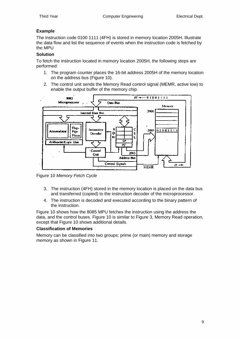
Example The instruction code 0100 1111 (4FH) is stored in memory location 2005H. Illustrate the data flow and list the sequence of events when the instruction code is fetched by the MPU Solution To fetch the instruction located in memory location 2005H, the following steps are performed:
1. The program counter places the 16-bit address 2005H of the memory location on the address bus (Figure 10).
2. The control unit sends the Memory Read control signal (MEMR, active low) to enable the output buffer of the memory chip.
Figure 10 Memory Fetch Cycle
3. The instruction (4FH) stored in the memory location is placed on the data bus and transferred (copied) to the instruction decoder of the microprocessor.
4. The instruction is decoded and executed according to the binary pattern of the instruction.
Figure 10 shows how the 8085 MPU fetches the instruction using the address the data, and the control buses. Figure 10 is similar to Figure 3, Memory Read operation, except that Figure 10 shows additional details. Classification of Memories Memory can be classified into two groups: prime (or main) memory and storage memory as shown in Figure 11.

Third Year Computer Engineering Electrical Dept.
10
Figure 11 Memory Classification R/WM (READ/WRITE MEMORY) As the name suggests, the microprocessor can write into or read from this memory; it is popularly known as Random Access memory (RAM). It is used primarily for information that is likely to be altered, such as writing programs or receiving data. This memory is volatile, meaning that when the power is turned off, all the contents are destroyed. Two types of R/W memories—static and dynamic—are available; they are described in the following paragraph. Static memory is made up of flip-flops, and it stores the bit as a voltage. Dynamic memory is made up of MOS transistor gates, and it stores the bit as a charge. The advantages of the dynamic memory are that it has high density and low power con-sumption and is cheaper than the static memory. The disadvantage is that the charge (bit information) leaks; therefore, stored information needs to be read and written again every few milliseconds. This is called refreshing the memory, and it requires extra circuitry, adding to the cost of the system. It is generally economical to use dynamic memory when the system memory size is at least 8K; for small systems, the static memory is appropriate. ROM (READ-ONLY MEMORY) The ROM is a nonvolatile memory; it retains stored information even if the power is turned off. This memory is used for programs and data that need not be altered. As the name suggests, the information can be read only, which means once a bit pattern is stored, it is permanent. The permanent group includes two types of memory: masked ROM and PROM. The semipermanent group also includes two types of memory: EPROM and EE-PROM, as shown in Figure 12. The concept underlying the ROM can be explained with the diodes arranged in a matrix format. The horizontal lines are connected to vertical lines only through the diodes.

Third Year Computer Engineering Electrical Dept.
11
Figure 12 Functional representation of ROM memory cell Each of the eight horizontal rows can be viewed as a register with binary addresses ranging from 000 to 111. The presence of a diode stores 1, and its absence stores 0. When a register, is selected, the voltage of that line goes high, and the output lines, where diodes are connected, go high. For example, when the memory register 111 is selected, the data byte 0111 1000 (78H) can be read at the data lines D7-D0. The diode representation is a simplified version of the actual MOSFET memory cell. Masked ROM In this ROM, a bit pattern is permanently recorded by the masking and metallization process. Memory manufacturers are generally equipped to do this process. It is an expensive and specialized process, but economical for large production quantities. PROM (Programmable Read-Only Memory): This memory has nichrome or polysilicon wires arranged in a matrix; these wires can be functionally viewed as diodes or fuses. This memory can be programmed by the user with a special PROM programmer that selectively burns line fuses according to the bit pattern to be stored. The process is known as "burning the PROM," and the information stored is permanent. EPROM (Erasable Programmable Read-Only Memory): This memory stores a bit by charging the floating gate of a FET. Information is stored by using an EPROM programmer, which applies high voltages to charge the gate. All the information can be erased by exposing the chip-to ultraviolet light through its quartz window, and the chip can be reprogrammed. Because the chip can be reused many times, this memory is ideally suited for product development, experimental projects, and college laboratories. The disadvantages of EPROM are (1) it must be taken out of the circuit to erase it, (2) the entire chip must be erased, and (3) the erasing process takes 15 to 20 minutes. EE-PROM (Electrically Erasable PROM): This memory is functionally similar to EPROM, except that information can be altered by using electrical signals at the register level rather than erasing all the information. This has an advantage in field and remote control applications. In microprocessor systems, software update is a common occurrence. If EE-PROMs are used in the systems, they can be updated from a central computer by using a remote link. This memory also includes a Chip Erase mode, whereby the entire chip can be erased in 10 ms vs. 15 to 20 min. to erase an EPROM. Flash Memory is a variation of EE-PROM. The major difference between the flash memory and EE-PROM is in the erasure procedure: the EE-PROM can be erased at a register level, but the flash memory must be erased in its entirety. However,

Third Year Computer Engineering Electrical Dept.
12
recently, some types of flash memory chips have become available that can be erased at a block (a group of registers) level. MICROPROCESSOR INSTRUCTION SET AND COMPUTER LANGUAGES Microprocessors recognize and operate in binary numbers. However, each microprocessor has its own binary words, meanings, and language. The words are formed by combining a number of bits for a given machine. The word (or word length) is defined as the number of bits the microprocessor recognizes and processes at a time. The word length ranges from four bits for small, microprocessor-based systems to 64 bits for high-speed large computers. Another term commonly used to express word length is byte. A byte is defined as a group of eight bits. 8085 Assembly Language Even though the instructions can be written in hexadecimal code, it is still difficult to understand a program written in hexadecimal numbers. Therefore, each manufacturer of a microprocessor has devised a symbolic code for each instruction, called a mnemonic. The mnemonic for a particular instruction consists of letters that suggest the operation to be performed by that instruction. For example, the binary code 0011 1100 (3C16 or 3CH in hexadecimal) of the 8085 microprocessor is represented by the mnemonic INR A: INR A INR stands for increment, and A represents the accumulator. This symbol suggests the operation of incrementing the
accumulator contents by one. Similarly, the binary code 1000 0000 (8016 or 80H) is represented as Although these symbols do not specify the complete operations, they suggest its significant pan. Machine language and assembly language are microprocessor-specific and are both considered low-level languages. INSTRUCTION FORMAT An instruction is a command to the microprocessor to perform a given task on specified data. Each instruction has two parts: one is the task to be performed, called the operation code (opcode), and the second is the data to be operated on, called the operand. The operand (or data) can be specified in various ways. It may include 8-bit (or 16-bit) data, an internal register, a memory location, or 8-bit (or 16-bit) address. In some instructions, the operand is implicit. Instruction Word Size The 8085 instruction set is classified into the following three groups according to word
1. One-word or 1-byte instructions 2. Two-word or 2-byte instructions 3. Three-word or 3-byte instructions
ONE-BYTE INSTRUCTIONS A 1-byte instruction includes the opcode and the operand in the same byte. For example:

Third Year Computer Engineering Electrical Dept.
13
Task Opcode Operand Binary Code Hex
Copy the contents of the accumulator in register C.
MOV C,A 0100 1111 4FH
Add the contents of register B to the contents of the accumulator.
ADD B 1000 0000 80 H
Invert (complement) each bit in the accumulator
CMA
0010 1111 2FH
These instructions are 1-byte instructions performing three different tasks. In the first instruction, both operand registers are specified. In the second instruction, the operand B is specified and the accumulator is assumed. Similarly, in the third instruction, the accumulator is assumed to be the implicit operand. TWO-BYTE INSTRUCTIONS In a 2-byte instruction, the first byte specifies the operation code and the second byte specifies the operand. For example:
Task Opcode Operand Binary Code
Hex
Load an 8-bit data byte in the accumulator
MVI A, Data 0011 1110 3E First Byte
DATA DATA Second Byte
Assume the data byte is 32H. The assembly language instruction is written as Mnemonics Hex Code MVI A.32H 3E 32H
THREE-BYTE INSTRUCTIONS In a 3-byte instruction, the first byte specifies the opcode, and the following two bytes specify the 16-bit address. Note that the second byte is the low-order address and the third byte is the high-order address. For example:
Task Opcode Operand Binary Code Hex Code
Transfer the Program sequence to the memory location 2085H.
JMP 2085H 1100 0011 C3 First Byte
1000 0101 85 Second Byte
0010 0000 20 Third Byte

Third Year Computer Engineering Electrical Dept.
14
ADDRESSING MODES These instructions, the source can be a register, an input port, or an 8-bit number (00H to FFH). Similarly, a destination can be a register or an output port. The sources and destination are, in fact, operands. The various formats of specifying the operands are called the addressing modes. The 8085 instruction set has the following addressing modes.
1. Immediate Addressing—MVI R.Data 2. Register Addressing—MOV Rd.Rs 3. Direct Addressing—IN/OUT Port# 4. Indirect Addressing
The classification of the addressing modes is unimportant, except that it provides some clues in understanding mnemonics. INSTRUCTION CLASSIFICATION An instruction is a binary pattern designed inside a microprocessor to perform a specific function. The entire group of instructions, called the instruction set, determines what functions the microprocessor can perform. The 8085 microprocessor includes the instruction set of its predecessor, the 8080A, plus two additional instructions. These instructions can be classified into DATA TRANSFER (COPY) OPERATIONS This group of instructions copies data from a location called a source to another location, called a destination, without modifying the contents of the source. The term data transfer is used for this copying function. However, the term transfer is misleading; it creates the impression that the contents of a source are destroyed when, in fact, the contents are retained without any modification. The various types of data transfer (copy) are listed below together with examples of each type: Type Examples Comment Between registers MOV D,B Copy the contents of register
B into register D.
Specific data byte to a register or a memory location.
MVI B,32 Load register B with the data byte 32H.
Between a memory location and a register
MOV B, M From the memory location M to register B.
Between an I/O device and the accumulator
IN Port #? From an input keyboard to the accumulator.
ARITHMETIC OPERATIONS These instructions perform arithmetic operations such as addition, subtraction, increment, and decrement.
• Addition—Any 8-bit number, or the contents of a register, or the contents of a memory location can be added to the contents of the accumulator and the sum is stored in the accumulator. No two other 8-bit registers can be added directly . The instruction DAD is an exception; it adds 16-bit data directly in register pairs.
• Subtraction—Any 8-bit number, or the contents of a register, or the contents
of a memory location can be subtracted from the contents of the accumulator and the results stored in the accumulator. The subtraction is performed in 2's
Third Year Computer Engineering Electrical Dept.
15
complement, and the results, if negative, are expressed in 2's complement. No two other registers can be subtracted directly.
• Increment/Decrement—The 8-bit contents of a register or a memory location can be incremented or decremented by 1. Similarly, the 16-bit contents of a register pair (such as BC) can be incremented or decremented by 1. These increment and decrement operations differ from addition and subtraction in an important way; i.e., they can be performed in any one of the registers or in a memory location.
LOGICAL OPERATIONS These instructions perform various logical operations with the contents of the accumulator.
• AND, OR, Exclusive-OR—Any 8-bit number, or the contents of a register, or a memory location can be logically ANDed, ORed, or Exclusive-ORed with the contents of the accumulator. The results are stored in the accumulator.
• Rotate—Each bit in the accumulator can be shifted either left or right to the next position.
• Compare—Any 8-bit number, or the contents of a register, or a memory location can be compared for equality, greater than, or less than, with the contents of the accumulator.
• Complement—The contents of the accumulator can be complemented; all 0s are replaced by 1’s and all 1’s are replaced by 0s.
BRANCHING OPERATIONS This group of instructions alters the sequence of program execution either conditionally or unconditionally.
• Jump—Conditional jumps are an important aspect of the decision-making process in programming. These instructions test for a certain condition (e.g.. Zero or Carry flag) and alter the program sequence when the condition is met. In addition, the instruction set includes an instruction called unconditional jump.
• Call, Return, and Restart—These instructions change the sequence of a program either by calling a subroutine or returning from a subroutine. The conditional Call and Return instructions also can test condition flags.
MACHINE CONTROL OPERATIONS These instructions control machine functions such as Halt, Interrupt, or do nothing. The 8085 Microprocessor The 8085A (commonly known as the 8085) is an 8-bit general-purpose microprocessor capable of addressing 64K of memory. The device has forty pins, requires a +5 V single power supply, and can operate with a 3-MHz single-phase clock. The 8085A-2 version can operate at the maximum frequency of 5 MHz. Figure 13 shows the logic pinout of the 8085 microprocessor. All the signals can be classified into six groups: (1) address bus, (2) data bus, (3) control and status signals, (4) power supply and frequency signals, (5) externally initiated signals, and (6) serial I/O ports.

Third Year Computer Engineering Electrical Dept.
16
Figure 13 The 8085 Microprocessor Pinout and Signals ADDRESS BUS The 8085 has eight signal lines, A15-A8 which are unidirectional and used as the high- order address bus. MULTIPLEXED ADDRESS/DATA BUS The signal lines AD7-AD0 are bidirectional: they serve a dual purpose. They are used as the low-order address bus as well as the data bus. In executing an instruction, during the earlier part of the cycle, these lines are used as the low-order address bus. During the later part of the cycle, these lines are used as the data bus, (This is also known as multiplexing the bus.) However, the low-order address bus can be separated from these signals by using a latch. CONTROL AND STATUS SIGNALS
This group of signals includes two control signals ( RD and WR ), three status signals-(IO/ M , S1 and S0) to identify the nature of the operation, and one special signal (ALE) to indicate the beginning of the operation. These signals are as follows:
• ALE—Address Latch Enable: This is a positive going pulse generated every time the 8085 begins an operation (machine cycle); it indicates that the bits on AD7-AD0 are address bits. This signal is used primarily to latch the low-order address from the multiplexed bus and generate a separate set of eight address lines, A7-A0.
• RD -Read: This is a Read control signal (active low). This signal indicates that the selected I/O or memory device is to be read and data are available on the data bus.
• WR -Write: This is a Write control signal (active low). This signal indicates that the data on the data bus are to be written into a selected memory or I/O location.
• IO/ M - This is a status signal used to differentiate between I/O and memory

Third Year Computer Engineering Electrical Dept.
17
operations. When it is high, it indicates an I/O operation; when it is low, it indicates a memory operation. This signal is combined with RD (Read) and WR (Write) to generate I/O and memory control signals.
• S1 and S0- These status signals, similar to IO/ M , can identify various operations, but they are rarely used in small systems. (All the operations and their associated status signals are listed in Table 1 for reference.)
TABLE 1 8085 Machine Cycle Status and Control Signals
Machine Cycle
Status
Control Signals IO/ M S1 S0
Opcode Fetch
Memory Read
Memory Write
I/O Read
I/O Write
Interrupt Acknowledge
Halt
Hold
Reset
0
0
0
1
1
1
Z
Z
Z
1
1
0
1
0
1
0
X
X
1
0
1
0
1
1
0
X
X
RD =0
RD =0
WR =0
RD =0
WR =0
INTA = 0
RD , WR = Z and INTA = 1
NOTE: Z- Tri-state (high impedance) X =■ Unspecified POWER SUPPLY AND CLOCK FREQUENCY The power supply and frequency signals are as follows:
• Vcc: +5 V power supply. • Vss: Ground Reference. • X1 X2: A crystal (or RC, LC network) is connected at these two pins. The
frequency is internally divided by two; therefore, to operate a system at 3 MHz. the crystal should have a frequency of 6 MHz.
• CLK (OUT)—Clock Output: This signal can be used as the system clock for other devices.
EXTERNALLY INITIATED SIGNALS, INCLUDING INTERRUPTS: The 8085 has five interrupt signals that can be used to interrupt a program execution. One of the signals, INTR (Interrupt Request), is identical to the 8080A microprocessor interrupt signal (INT); the others are enhancements to the 8080A. The microprocessor acknowledges an interrupt request by the INTA (Interrupt Acknowledge) signal. In addition to the interrupts, three pins—RESET, HOLD, and READY—accept the externally initiated signals as inputs. To respond to the HOLD request, it has one signal called HLDA (Hold Acknowledge).
Third Year Computer Engineering Electrical Dept.
18
• : When the signal on this pin goes low, the program counter is set to zero, the buses are tri-stated, and the MPU is reset.
• RESET OUT: This signal indicates that the MPU is being reset. The signal can be used to reset other devices.
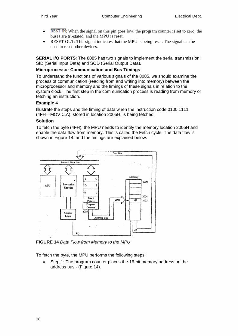
SERIAL I/O PORTS: The 8085 has two signals to implement the serial transmission: SID (Serial Input Data) and SOD (Serial Output Data). Microprocessor Communication and Bus Timings To understand the functions of various signals of the 8085, we should examine the process of communication (reading from and writing into memory) between the microprocessor and memory and the timings of these signals in relation to the system clock. The first step in the communication process is reading from memory or fetching an instruction. Example 4 Illustrate the steps and the timing of data when the instruction code 0100 1111 (4FH—MOV C,A), stored in location 2005H, is being fetched. Solution To fetch the byte (4FH), the MPU needs to identify the memory location 2005H and enable the data flow from memory. This is called the Fetch cycle. The data flow is shown in Figure 14, and the timings are explained below.
FIGURE 14 Data Flow from Memory to the MPU To fetch the byte, the MPU performs the following steps:
• Step 1: The program counter places the 16-bit memory address on the address bus - (Figure 14).

Third Year Computer Engineering Electrical Dept.
19
FIGURE 15 Timing: Transfer of Byte from Memory to MPU Figure 15 shows that at T1 the high-order memory address 20H is placed on the address lines A15-A8, the low-order memory address 05H is placed on the bus AD7-AD0, and the ALE signal goes high. Similarly, the status signal IO/ goes low, indicating that this is a memory-related operation. (For the sake of clarity, the other two status signals, S1 and S0, are not shown in Figure 15).
• Step 2: The control unit sends the control signal to enable the memory chip (Figure 14).
The control signal is sent out during the clock period T2, thus enabling the memory chip. The is active during two clock periods.
• Step 3: The byte from the memory location is placed on the data bus. When the memory is enabled, the instruction byte (4FH) is placed on the bus AD7-AD0 and transferred to the microprocessor. The signal causes 4FH to be placed on bus AD7-AD0 (shown by the arrow), and when goes high, it causes the bus to go into high impedance.
• Step 4: The byte is placed in the instruction decoder of the microprocessor, and the task is carried out according to the instruction.
The machine code or the byte (4FH) is decoded by the instruction decoder, and the contents of the accumulator are copied into register C. This task is performed during the period T4 in Figure 15. Example Illustrate the timing diagram for executing the following instruction MVI A, 32H Solution To illustrate the Memory Read machine cycle, we need to examine the execution of a 2-byte instruction. Two machine codes 00111110 (3EH) and 0011 0010 (32H) are stored in memory locations 2000H and 2001H. The first machine code (3EH) represents the opcode to

Third Year Computer Engineering Electrical Dept.
20
load a data byte in the accumulator, and the second code (32H) represents the data byte to be loaded in the accumulator. The timings diagram is shown in Figure (16) The diagram shows the following
1. The first machine cycle M1(Opcode Fetch) is identical in bus timings with the machine cycle illustrated in Example 3, except for the bus contents.
FIGURE 16 Timing for Execution of the Instruction MVI A.32H
2. After completion of the Opcode Fetch cycle, the 8085 places the address 2001H on the address bus and increments the program counter to the next address 2002H. The second machine cycle M2 is identified as the Memory Read cycle (IO/ =0, S1 = 1, and S0=0) and the ALE is asserted. At T2, the
signal becomes active and enables the memory chip. 3. At the rising edge of T2, the 8085 activates the data bus as an input bus;
memory places the data byte 32H on the data bus, and the 8085 reads and stores the byte in the accumulator during T3.
Instruction cycle is defined as the time required to complete the execution of an instruction. The 8085 instruction cycle consists of one to six machine cycles or one to six operations. Machine cycle is defined as the time required to complete one operation of accessing memory, I/O, or acknowledging an external request. This cycle may consist of three to six T-states. In Figure 15, the instruction cycle and the machine cycle are the same. . T-state is defined as one subdivision of the operation performed in one clock period. How to Recognize Machine Cycles In the last two examples, the number of bytes is the same as the number of machine cycles. However, there is no direct relationship between the number of bytes in an instruction and the number of machine cycles required to execute that instruction. This is illustrated in the following example. Example: Explain the machine cycles of the following 3-byte instruction when it is executed.

Third Year Computer Engineering Electrical Dept.
21
Machine Opcode Operand Bytes Cycles T-States Operation
STA 2065H 3 4 13 This instruction stores (writes) the contents of the accumulator in memory location 2065H
Solution Memory Address Machine Code
2010 2011 2012
0011 0010 → 0110 0101 → 0010 0000 →
32H 65H 20H
Opcode Low-order address High-order address
This is a 3-byte instruction; however, it has four machine cycles with 13 T-states. The first operation in the execution of an instruction must be an Opcode Fetch. The 8085 requires three T-states for each subsequent operation; thus, nine T-states are required for the remaining machine cycles. Therefore, the Opcode Fetch in this instruction must be a four T-state machine cycle, the same as the one described in the previous example. The two machine cycles following the Opcode Fetch must be Memory Read machine cycles because the microprocessor must read all the machine codes (three bytes) before it can execute the instruction. Now let us examine what the instruction does. It stores (writes) the contents of the accumulator in memory location 2065H; therefore, the last machine cycle must be Memory Write. The execution steps are as follows:
1. In the first machine cycle, the 8085 places the address 2010H on the address bus and fetches the opcode 32H.
2. The second machine cycle is Memory Read. The processor places the address 2011H and gets the low-order byte 65H.
3. The third machine cycle is also Memory Read; the 8085 gets the high-order byte 20H from memory location 2012H.
4. The last machine cycle is Memory Write. The 8085 places the address 2065H on the address bus, identifies the operation as Memory Write (IO/ =0, S1= 0, and S0 =1). It places the contents of the accumulator on the data bus AD7-AD0 and asserts the signal. During the last T-state, the contents of the data bus are placed in memory location 2065H.
COUNTERS AND TIME DELAYS Designing a counter is a frequent programming application. Counters are used primarily to keep track of events; time delays are important in setting up reasonably accurate timing between two events. The process of designing counters and time delays using software instructions is far more flexible and less time consuming than the design process using hardware. COUNTER A counter is designed simply by loading an appropriate number into one of the registers and using the INR (Increment by One) or the DCR (Decrement by One) instructions. A loop is established to update the count, and each count is checked to determine whether it has reached the final number; if not, the loop is repeated. The flowchart shown in Figure 17 illustrates these steps. However, this counter has one major drawback; the counting is performed at such high speed that only the last count can be observed. To observe counting, there must be an appropriate time

Third Year Computer Engineering Electrical Dept.
22
delay between counts.
FIGURE 17 Flowchart of a Counter TIME DELAY The procedure used to design a specific delay is similar to that used to set up a counter. A register is loaded with a number, depending on the time delay required, and then the register is decremented until it reaches zero by setting up a loop with a conditional Jump instruction. The loop causes the delay, depending upon the clock period of the system.
Time Delay Using One Register The flowchart in Figure 18 shows a time-delay loop. A count is loaded in a register, and the loop is executed until the count reaches zero. The set of instructions necessary to set up the loop is also shown in Figure 18.
FIGURE 18 Time Delay Loop: Flowchart and Instructions The last column in Figure 18 shows the T-states (clock periods) required by the 8085 microprocessor to execute each instruction. The instruction MVI requires seven clock periods. An 8085-based microcomputer with 2 MHz clock frequency will execute the instruction MVI in 3.5 µs as follows: Clock frequency of the system f = 2 MHz
Clock period T = 1/f = × 10-6 = 0.5 µs
Time to execute MVI = 7 T-states x 0.5 = 3.5 µs TL = (T × Loop T-states x N10) where TL = Time delay in the loop T = System clock period

Third Year Computer Engineering Electrical Dept.
23
N10 = Equivalent decimal number of the hexadecimal count loaded in the delay register TL = (0.5 x 10-6 x 14 x 255) = 1785 µs ≈1.8 ms Time Delay Using a Register Pair The time delay can be considerably increased by setting a loop and using a register pair with a 16-bit number (maximum FFFFH). The 16-bit number is decremented by using the instruction DCX. However, the instruction DCX does not set the zero flag, without the test flags. Jump instructions cannot check desired data conditions. Additional techniques, therefore, must be used to set the Zero flag. The following set of instructions uses a register pair to set up a time delay. Label Opcode Operand Comments T-states
LXl B, 2384H ;Load BC with 16-bit count 10 LOOP: DCX B ;Decrement (BC) by one 6 MOV A, C ;Place contents of C in A 4 ORA B ;OR (B) with (A) to set Zero flag 4 JNZ LOOP ; If result ≠ 0. jump back to LOOP 10/7 In this set of instructions, the instruction LXI B, 2384H loads register B with the number 23H, and register C with the number 84H. The instruction DCX decrements the entire number by one (e.g., 2384H becomes 2383H). The next two instructions are used only to set the Zero flag: otherwise, they have no function in this problem. The OR instruction sets the Zero flag only when the contents of B and C are simultaneously zero. Therefore, the loop is repeated 2384H times, equal to the count set in the register pair. Time Delay The time delay in the loop is calculated as in the previous example. The loop includes four instructions: DCX, MOV, ORA, and JNZ, and takes 24 clock periods for execution. The loop is repeated 2384H times, which is converted to decimals as 2384H = 2 x (16)3 + 3 x (16)2 + 8 x (16)1 + 4(16)0 = 909210
If the clock period of the system 0.5 µs, the delay in the loop T1 is TL = (0.5 x 24 x 909210) ≈109 ms (without adjusting for the last cycle) Total Delay TD = 109 ms + T0 ≈109 ms (The instruction LXI adds only 5 µs.) A similar time delay can be achieved by using the technique of two loops Time Delay Using a Loop within a Loop Technique A time delay similar to that of a register pair can also be achieved by using two loops; one loop inside the other loop, as shown in Figure 19. For example, register C is used in the inner loop (LOOP1) and register B is used for the outer loop (LOOP2). The following instructions can be used to implement the flowchart shown in Figure 19(a). MVI B, 38H 7T LOOP2: MVI C, FFH 7T LOOP1: DCR C 4T

Third Year Computer Engineering Electrical Dept.
24
JNZ LOOP1 10/7T DCR B 4T JNZ LOOP2 10/7T Delay Calculations. The delay in LOOP1 is TL1= 1783.5 µs. We can replace LOOP1 by TL1, as shown in Figure 19(b). Now we can calculate the delay in LOOP2 as if it is one loop; this loop is executed 56 times because of the count (38H) in register B: TL2 = 56(TL1 + 21 T-states x 0.5 µs) = 56(1783.5 µs+ 10.5 µs) = 100.46 ms
FIGURE 19 Flowchart for Time Delay with Two Loops Additional Techniques for Time Delay The disadvantages in using software delay techniques for real-time applications in which the demand for time accuracy is high, such as digital clocks, are as follows:
1. The accuracy of the time delay depends on the accuracy of the system's clock.
2. The microprocessor is occupied simply in a waiting loop; otherwise it could be employed to perform other functions.
3. The task of calculating accurate time delays is tedious. In real-time applications, timers (integrated timer circuits) are commonly used.
a b

Third Year Computer Engineering Electrical Dept.
25
Interrupts The interrupt I/O is a process of data transfer whereby an external device or a peripheral can inform the processor that it is ready for communication and it requests attention. The process is initialed by an external device and is asynchronous, meaning that it can be initiated at any lime without reference to the system clock. However, the response to an interrupt request is directed or controlled by the microprocessor. The interrupt requests are classified in two categories: maskable interrupt and nonmaskable interrupt. The 8085 microprocessor includes four maskable interrupts and one nonmaskable interrupt. Among the four maskable interrupts, one is non-vectored, which requires external hardware to supply a Call location to restart the execution. The other three are vectored to specific locations. The 8085 interrupt process can be described in terms of those eight steps. Step 1: The interrupt process should be enabled by writing the instruction EI in the
main program. The instruction EI sets the Interrupt Enable flip-flop. The instruction DI resets the flip-flop and disables the interrupt process. Instruction EI (Enable Interrupt)
• This is a 1-byte instruction. • The instruction sets the Interrupt Enable flip-flop and enables the
interrupt process. • System reset or an interrupt disables the interrupt process.
Instruction DI (Disable Interrupt) • This is a 1-byte instruction. • The instruction resets the Interrupt Enable flip-flop and disables the
interrupt. • It should be included in a program segment where an interrupt from an
outside source cannot be tolerated. Step 2: When the microprocessor is executing a program, it checks the INTR line
during the execution of each instruction. Step 3: If the line INTR is high and the interrupt is enabled, the microprocessor
completes the current instruction, disables the Interrupt Enable flip-flop and sends a signal called INTA—Interrupt Acknowledge (active low). The processor cannot accept any interrupt requests until the interrupt flip-flop is enabled again.
Step 4: The signal INTA is used to insert a restart (RST) instruction (or a Call in-struction) through external hardware. The RST instruction is a 1-byte call in-struction that transfers the program control to a specific memory location on page 00H and restarts the execution at that memory location after executing Step 5.
Step 5: When the microprocessor receives an RST instruction (or a Call instruction), it saves the memory address of the next instruction on the stack. This is simi-lar to inserting a bookmark. The program is transferred to the CALL location.
Step 6: Assuming that the task to be performed is written as a subroutine at the specified location, the processor performs the task. This subroutine is known as a service routine.
Step 7: The service routine should include the instruction EI to enable the interrupt again. This is similar to putting the receiver back on the hook.
Step 8: At the end of the subroutine, the RET instruction retrieves the memory address where the program was interrupted and continues the execution.

Third Year Computer Engineering Electrical Dept.
26
RST (RESTART) INSTRUCTIONS The 8085 instruction set includes eight RST (Restart) instructions. These are 1-byte Call instructions and transfer the program execution to a specific location on page 00H. as listed in Table 3. The RST instructions are executed in a similar way to that of Call instructions. The address in the program counter (meaning the address of the next instruction to an RST instruction) is stored on the stack before the program execution is transferred to the RST call location. When the processor encounters a Return instruction in the subroutine associated with the RST instruction, the program returns to the address that was stored on the stack. In case of a hardware interrupt, we will use an RST instruction to restart the program execution. Table 3 Restart Instructions
Mnemonics
Binary Code
Hex Code Call Locution In Hex D7 D6 D5 D4 D3 D2 D1 D0 RST 0 1 1 0 0 0 1 1 1 C7 0000 RST 1 1 1 0 0 1 1 1 1 CF 0008 RST 2 1 1 0 1 0 1 1 1 D7 0010 RST 3 1 1 0 1 1 1 1 1 DF 0018 RST 4 1 1 1 0 0 1 1 1 E7 0020 RST 5 1 1 1 0 1 1 1 1 EF 0028 RST 6 1 1 1 1 0 1 1 1 F7 0030 RST 7 1 1 1 1 1 1 1 1 FF 0038 To implement Step 4 in the interrupt process, insert one of these instructions in the microprocessor by using external hardware and the signal (Interrupt Acknowledge), as shown in Figure 20.
FIGURE 20 A circuit to Implement the Instruction RST 5 In Figure 20, the instruction RST 5 is built using resistors and a tri-state buffer. Figure 21 shows the timing of the 8085 Interrupt Acknowledge machine cycle. In response to the INTR (Interrupt Request) high signal, the 8085 sends the (Interrupt Acknowledge) low signal, which is used to enable the buffer, and the RST instruction is placed on the data bus during M1. During M1, the program counter holds the memory address of the next instruction, which should be stored on the stack so that the program can continue after the service routine. During M2, the address of the

Third Year Computer Engineering Electrical Dept.
27
stack pointer minus one (SP - 1) location is placed on the address bus, and the high-order address of the program counter is stored on the stack. During M3, the low-order address of the program counter is stored in the next location (SP - 2) of the stack.
FIGURE 21 8085 Timing of the Interrupt Acknowledge Machine Cycle and Execution of an RST Instruction The machine cycle M| of the Interrupt Acknowledge is identical with the Opcode Fetch cycle, with two exceptions. The signal is sent out instead of the signal, and the status lines (IO/ , S0 and S1) are 1 1 1 instead of 0 1 1 (see Figure 21). During M1, the RST 5 is decoded, a 1-byte Call instruction to location 0028H. The machine cycles M1 and M3 are Memory Write cycles that store the contents of the program counter on the stack, and then a new instruction cycle begins. In this next instruction cycle, the program is transferred to location 0028H. The service routine is written somewhere else in memory, and the Jump instruction is written at 0028H to specify the address of the service routine. All these steps are illustrated in the following example. Example 7 Illustration: An Implementation of the 8085 Interrupt PROBLEM STATEMENT
1. Write a main program to count continuously in binary with a one-second delay between each count.
2. Write a service routine at XX70H to flash FFH five times when the program is interrupted, with some appropriate delay between each flash.
MAIN PROGRAM Memory ADDRESS
Label Mnemonics Comments
XX00 LXI SP, XX99H ;initialize stack pointer
03 EI ;Enable interrupt process
AD0

Third Year Computer Engineering Electrical Dept.
28
04 MVI A, 00H ;Initialize counter
06 NXTCNT: OUT PORT 1 ;display count
08 MV1 C, 01 H ;Parameter for 1-second delay
0A CALL DELAY ;Wait one second
0D INR A ;Next count
0E JMP NXTCNT ; Continue
Delay Routine: Use delay subroutine Service Routine Memory ADDRESS
Label Mnemonics Comments
XX70 SERV: PUSH B ;Save contents
71 PUSH PSW
72 MVI B, 0AH ;Load register B for five flashes and five blanks
74 MVI A, 00 H ;Loads 00 to blank display
76 FLASH: OUT PORT 1
78 MVI C, 01H ; Parameter for 1 second delay
7A CALL DELAY:
7D CMA ; Complement display count
7E DCR B ;Reduce count
7F JNZ FLASH
82 POP PSW
83 POP B
84 EI ;Enable Interrupts process
85 RET ; service is complete, go back ;to main program
DESCRIPTION OF THE INTERRUPT PROCESS 1. The main program initializes the stack pointer at XX99H and enables the
interrupts. The program will count continuously from 00H to FFH, with a delay of one second between each count.
2. To interrupt the processor, push the switch. The INTR line goes high. 3. Assuming the switch is pushed when the processor is executing the

Third Year Computer Engineering Electrical Dept.
29
instruction OUT at memory location XX06H, the following sequence of events occurs.
a) The microprocessor completes the execution of the instruction OUT. b) It senses that the line INTR is high, and that the interrupt is enabled. c) The microprocessor disables the interrupt, stops execution, and sends
out a control signal (Interrupt Acknowledge). d) The (active low) enables the tri-state buffer, and the instruction
EFH is placed on the data bus. e) The microprocessor saves the address XX08H of the next instruction
(MVI C, 01H) on the stack at locations XX98H and XX97H. and the program is transferred to memory location 0028H. The locations 0028-29-2AH should have the following Jump instruction to transfer the program to the service routine.
JMP XX70H (However, you do not have access to write at 0028H in the monitor program.
4. The program jumps to the service routine at XX70H. 5. The service routine saves the registers that are being used in the subroutine
and loads the count ten in register B to output five flashes and also five blanks.
6. The service routine enables the interrupt before returning to the main program.
7. When the service routine executes the RET instruction, the microprocessor retrieves the memory address XX08H from the top of the stack and continues the binary counting.
VECTORED INTERRUPTS The 8085 has five interrupt inputs. One is called INTR, three are called RST 5.5, 6.5, and 7.5, respectively, and the fifth is called TRAP, a nonmaskable interrupt. These last four (RSTs and TRAP) are automatically vectored (transferred) to specific locations on memory page 00H without any external hardware. They do not require the signal or an input port; the necessary hardware is already implemented inside the 8085. These interrupts and their call locations are as follows:
Interrupts Call Locations 1. TRAP 0024H 2. RST 7.5 003CH 3. RST 6.5 0034H 4. RST 5.5 002CH

Third Year Computer Engineering Electrical Dept.
30
The TRAP has the highest priority, followed by RST 7.5, 6.5, 5.5. and INTR, in that order; however, the TRAP has a lower priority than the Hold signal used for DMA
FIGURE 21 The 8085 Interrupts and Vector Locations TRAP TRAP, a nonmaskable interrupt known as NMI. It has the highest priority among the interrupt signals, it need not be enabled, and it cannot be disabled. It is level- and edge-sensitive, meaning that the input should go high and stay high to be acknowledged. It cannot be acknowledged again until it makes a transition from high to low to high. Figure 21 shows that when this interrupt is triggered, the program control is transferred to location 0024H without any external hardware or the interrupt enable instruction EI. TRAP is generally used for such critical events as power failure and emergency shut-off. 12.22 RST 7.5, 6.5, and 5.5 These maskable interrupts (shown in Figure 21) are enabled under program control with two instructions: EI (Enable Interrupt) described earlier, and SIM (Set Interrupt Mask) described below: Instruction SIM: Set Interrupt Mask. This is a 1-byte instruction and can be used for three different functions (Figure 22).
• One function is to set mask for RST 7.5, 6.5, and 5.5 interrupts. This instruction reads the content of the accumulator and enables or disables the interrupts according to the content of the accumulator. Bit D3 is a control bit and should = 1 for bits D0, D1, and D2 to be effective. Logic 0 on D0, D1, and D2 will enable the corresponding interrupts, and logic 1 will disable the interrupts.

Third Year Computer Engineering Electrical Dept.
31
FIGURE 22 Interpretation of the Accumulator Bit Pattern for the SIM Instruction
• The second function is to reset RST 7.5 flip-flop (Figure 22). Bit D4 is additional control for RST 7.5. If D4 = 1, RST 7.5 is reset. This is used to override (or ignore) RST 7.5 without servicing it
• The third function is to implement serial I/O. Bits D7 and D6 of the accumulator are used for serial I/O and do not affect the interrupts. Bit D6 = 1 enables the serial I/O and bit D7 is used to transmit (output) bits.
TRIGGERING LEVELS These interrupts are sensitive to different types of triggering as listed below:
• RST 7.5: This is positive-edge sensitive and can be triggered with a short pulse. The request is stored internally by the D flip-flop (Figure 21) until the microprocessor responds to the request or until it is cleared by Reset or by bit D4 in SIM instruction.
• RST 6.5 and RST 5.5: These interrupts are level-sensitive, meaning that the triggering level should be on until the microprocessor completes the execution of the current instruction. If the microprocessor is unable to respond to these requests immediately, they should be stored or held by external hardware.
Example 8: Enable all the interrupts in an 8085 system. Solution: Instructions
EI ;Enable interrupts MVI A, 08H ;Load bit pattern to enable RST 7.5, 6.5, and 5.5 SIM ;Enable RST 7.5, 6.5, and 5.5
Bit D3 = 1 in the accumulator makes the instruction SIM functional, and bits D2, D1, and D0 = 0 enable the interrupts 7.5, 6.5, and 5.5. Example 9: Reset the 7.5 interrupt from Example 8 Solution: Instructions
MVI A, 18H ;Set D4 = 1 SIM ;Reset 7.5 interrupt flip-flop
PENDING INTERRUPTS

Third Year Computer Engineering Electrical Dept.
32
Because there are several interrupt lines, when one interrupt request is being served, other interrupt requests may occur and remain pending. The 8085 has an additional instruction called RIM (Read Interrupt Mask) to sense these pending interrupts. Instruction RIM: Read Interrupt Mask. This is a 1 -byte instruction and can be used for the following functions.
• To read interrupt masks. This instruction loads the accumulator with 8 bits indicating the current status of the Interrupt masks (Figure 23).
• To identify pending interrupts. Bits D4, D5, and D6 (Figure 23) identify the pending interrupts.
• To receive serial data. Bit D7 (Figure 23) is used to receive serial data.
FIGURE 23 Interpretation of the Accumulator Bit Pattern for the RIM Instruction Example 10 Assuming the microprocessor is completing an RST 7.5 interrupt request, check to see if RST 6.5 is pending. If it is pending, enable RST 6.5 without affecting any other interrupts; otherwise, return to the main program. Solution: Instructions
The instruction RIM checks for a pending interrupt. Instruction ANI 20H masks all the bits except D5 to check pending RST 6.5. If D5 = 0, the program control is transferred to the main program. D5 = 1 indicates that RST 6.5 is pending. Instruction ANI 0DH sets D1 = 0 (RST 6.5 bit for SIM), instruction ORI sets D3 = 1 (this is necessary for SIM to be effective), and instruction SIM enables RST 6.5 without affecting any other interrupts. The JMP instruction transfers the program to the service routine (SERV) written for RST 6.5.