Embed Size (px)
Citation preview
Introduction toCMOS VLSI
Design
Test

Test Slide 2CMOS VLSI Design
Outline Testing
– Logic Verification– Silicon Debug– Manufacturing Test
Fault Models Observability and Controllability Design for Test
– Scan– BIST
Boundary Scan

Test Slide 3CMOS VLSI Design
Testing Testing is one of the most expensive parts of chips
– Logic verification accounts for > 50% of design effort for many chips
– Debug time after fabrication has enormous opportunity cost
– Shipping defective parts can sink a company
Example: Intel FDIV bug– Logic error not caught until > 1M units shipped– Recall cost $450M (!!!)

Test Slide 4CMOS VLSI Design
Logic Verification Does the chip simulate correctly?
– Usually done at HDL level– Verification engineers write test bench for HDL
• Can’t test all cases• Look for corner cases• Try to break logic design
Ex: 32-bit adder– Test all combinations of corner cases as inputs:
• 0, 1, 2, 231-1, -1, -231, a few random numbers Good tests require ingenuity
Test Slide 5CMOS VLSI Design
Silicon Debug Test the first chips back from fabrication
– If you are lucky, they work the first time– If not…
Logic bugs vs. electrical failures– Most chip failures are logic bugs from inadequate
simulation– Some are electrical failures
• Crosstalk• Dynamic nodes: leakage, charge sharing• Ratio failures
– A few are tool or methodology failures (e.g. DRC) Fix the bugs and fabricate a corrected chip

Test Slide 6CMOS VLSI Design
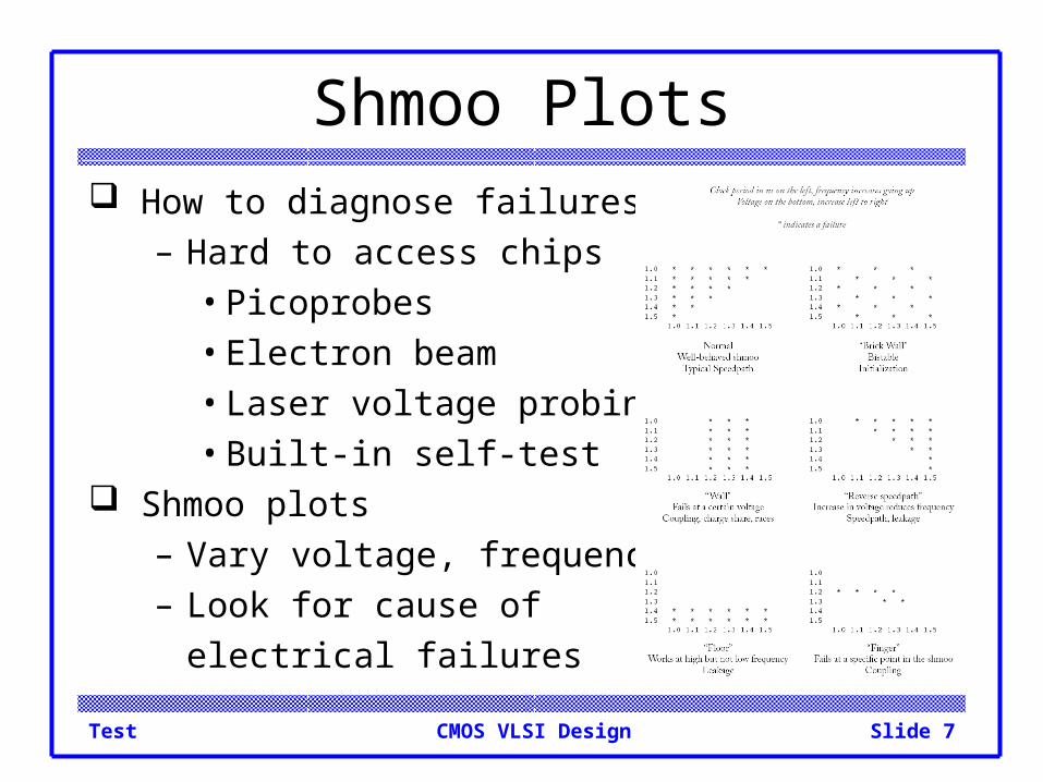
Shmoo Plots How to diagnose failures?
– Hard to access chips• Picoprobes• Electron beam• Laser voltage probing• Built-in self-test
Shmoo plots– Vary voltage, frequency– Look for cause of
electrical failures
Test Slide 7CMOS VLSI Design
Shmoo Plots How to diagnose failures?
– Hard to access chips• Picoprobes• Electron beam• Laser voltage probing• Built-in self-test
Shmoo plots– Vary voltage, frequency– Look for cause of
electrical failures

Test Slide 8CMOS VLSI Design
Manufacturing Test A speck of dust on a wafer is sufficient to kill chip Yield of any chip is < 100%
– Must test chips after manufacturing before delivery to customers to only ship good parts
Manufacturing testers are
very expensive– Minimize time on tester– Careful selection of
test vectors
Test Slide 9CMOS VLSI Design
Cheap Testers If you don’t have a multimillion dollar tester:
– Build a breadboard with LED’s and switches– Hook up a logic analyzer and pattern generator– Or use a low-cost functional chip tester

Test Slide 10CMOS VLSI Design
TestosterICs Ex: TestosterICs functional chip tester
– Reads test vectors, applies them to your chip, and reports assertion failures
Test Slide 11CMOS VLSI Design
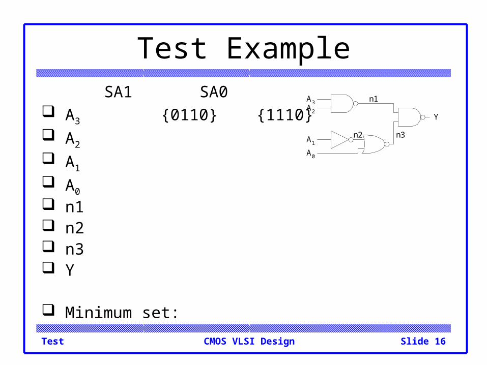
Stuck-At Faults How does a chip fail?
– Usually failures are shorts between two conductors or opens in a conductor
– This can cause very complicated behavior A simpler model: Stuck-At
– Assume all failures cause nodes to be “stuck-at” 0 or 1, i.e. shorted to GND or VDD
– Not quite true, but works well in practice
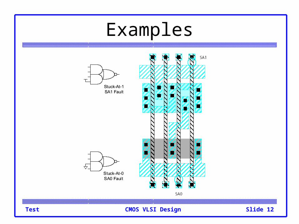
Test Slide 12CMOS VLSI Design
Examples
Test Slide 13CMOS VLSI Design
Observability & Controllability
Observability: ease of observing a node by watching external output pins of the chip
Controllability: ease of forcing a node to 0 or 1 by driving input pins of the chip
Combinational logic is usually easy to observe and control
Finite state machines can be very difficult, requiring many cycles to enter desired state– Especially if state transition diagram is not known
to the test engineer
Test Slide 14CMOS VLSI Design
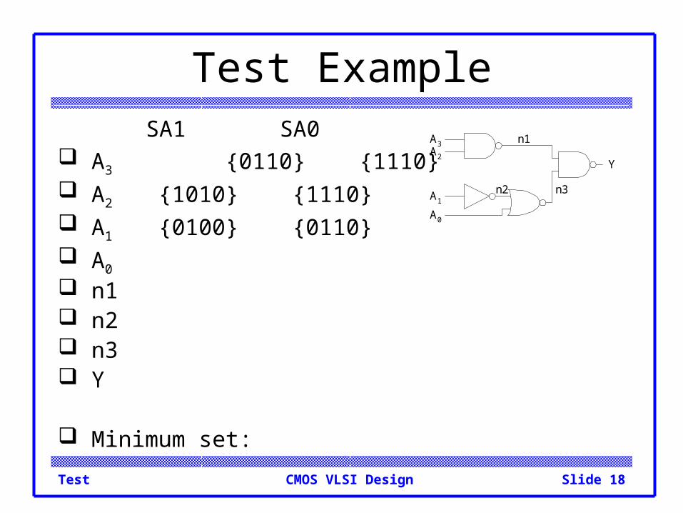
Test Pattern Generation Manufacturing test ideally would check every node in
the circuit to prove it is not stuck. Apply the smallest sequence of test vectors
necessary to prove each node is not stuck.
Good observability and controllability reduces number of test vectors required for manufacturing test.– Reduces the cost of testing– Motivates design-for-test
Test Slide 15CMOS VLSI Design
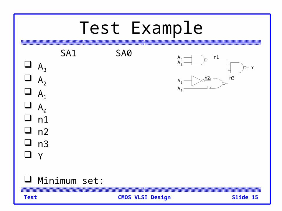
Test ExampleSA1 SA0
A3 A2
A1
A0
n1 n2 n3 Y
Minimum set:
A3A2
A1
A0
Y
n1
n2 n3
Test Slide 16CMOS VLSI Design
Test ExampleSA1 SA0
A3 {0110} {1110} A2
A1
A0
n1 n2 n3 Y
Minimum set:
A3A2
A1
A0
Y
n1
n2 n3

Test Slide 17CMOS VLSI Design
Test ExampleSA1 SA0
A3 {0110} {1110} A2 {1010} {1110} A1
A0
n1 n2 n3 Y
Minimum set:
A3A2
A1
A0
Y
n1
n2 n3
Test Slide 18CMOS VLSI Design
Test ExampleSA1 SA0
A3 {0110} {1110} A2 {1010} {1110} A1 {0100} {0110} A0
n1 n2 n3 Y
Minimum set:
A3A2
A1
A0
Y
n1
n2 n3

Test Slide 19CMOS VLSI Design
Test ExampleSA1 SA0
A3 {0110} {1110} A2 {1010} {1110} A1 {0100} {0110} A0 {0110} {0111} n1 n2 n3 Y
Minimum set:
A3A2
A1
A0
Y
n1
n2 n3
Test Slide 20CMOS VLSI Design
Test ExampleSA1 SA0
A3 {0110} {1110} A2 {1010} {1110} A1 {0100} {0110} A0 {0110} {0111} n1 {1110} {0110} n2 n3 Y
Minimum set:
A3A2
A1
A0
Y
n1
n2 n3
Test Slide 21CMOS VLSI Design
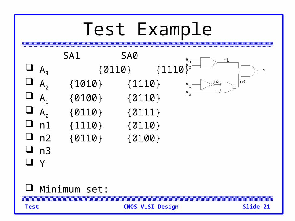
Test ExampleSA1 SA0
A3 {0110} {1110} A2 {1010} {1110} A1 {0100} {0110} A0 {0110} {0111} n1 {1110} {0110} n2 {0110} {0100} n3 Y
Minimum set:
A3A2
A1
A0
Y
n1
n2 n3
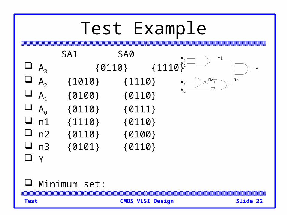
Test Slide 22CMOS VLSI Design
Test ExampleSA1 SA0
A3 {0110} {1110} A2 {1010} {1110} A1 {0100} {0110} A0 {0110} {0111} n1 {1110} {0110} n2 {0110} {0100} n3 {0101} {0110} Y
Minimum set:
A3A2
A1
A0
Y
n1
n2 n3
Test Slide 23CMOS VLSI Design
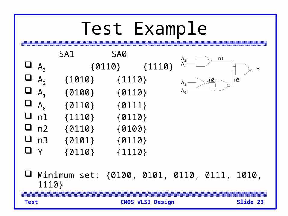
Test ExampleSA1 SA0
A3 {0110} {1110} A2 {1010} {1110} A1 {0100} {0110} A0 {0110} {0111} n1 {1110} {0110} n2 {0110} {0100} n3 {0101} {0110} Y {0110} {1110}
Minimum set: {0100, 0101, 0110, 0111, 1010, 1110}
A3A2
A1
A0
Y
n1
n2 n3
Test Slide 24CMOS VLSI Design
Design for Test Design the chip to increase observability and
controllability
If each register could be observed and controlled, test problem reduces to testing combinational logic between registers.
Better yet, logic blocks could enter test mode where they generate test patterns and report the results automatically.

Test Slide 25CMOS VLSI Design
Scan Convert each flip-flop to a scan register
– Only costs one extra multiplexer Normal mode: flip-flops behave as usual Scan mode: flip-flops behave as shift register
Contents of flops
can be scanned
out and new
values scanned
in
Flo
p
QD
CLK
SI
SCAN
scan out
scan-in
inputs outputs
Flo
pF
lop
Flo
pF
lop
Flo
pF
lop
Flo
pF
lop
Flo
pF
lop
Flo
pF
lop
LogicCloud
LogicCloud

Test Slide 26CMOS VLSI Design
Scannable Flip-flops
0
1 Flo
p
CLK
D
SI
SCAN
Q
D
X
Q
Q
(a)
(b)
SCAN
SI
D
X
Q
Q
SI
s
s
(c)
d
d
d
s
SCAN

Test Slide 27CMOS VLSI Design
Built-in Self-test Built-in self-test lets blocks test themselves
– Generate pseudo-random inputs to comb. logic– Combine outputs into a syndrome– With high probability, block is fault-free if it
produces the expected syndrome
Test Slide 28CMOS VLSI Design
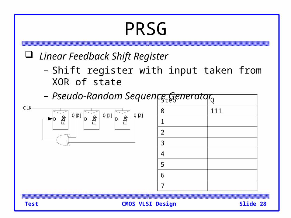
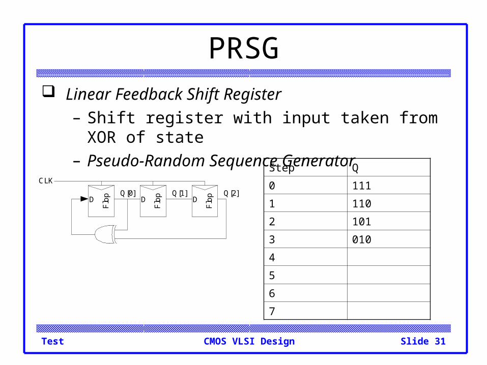
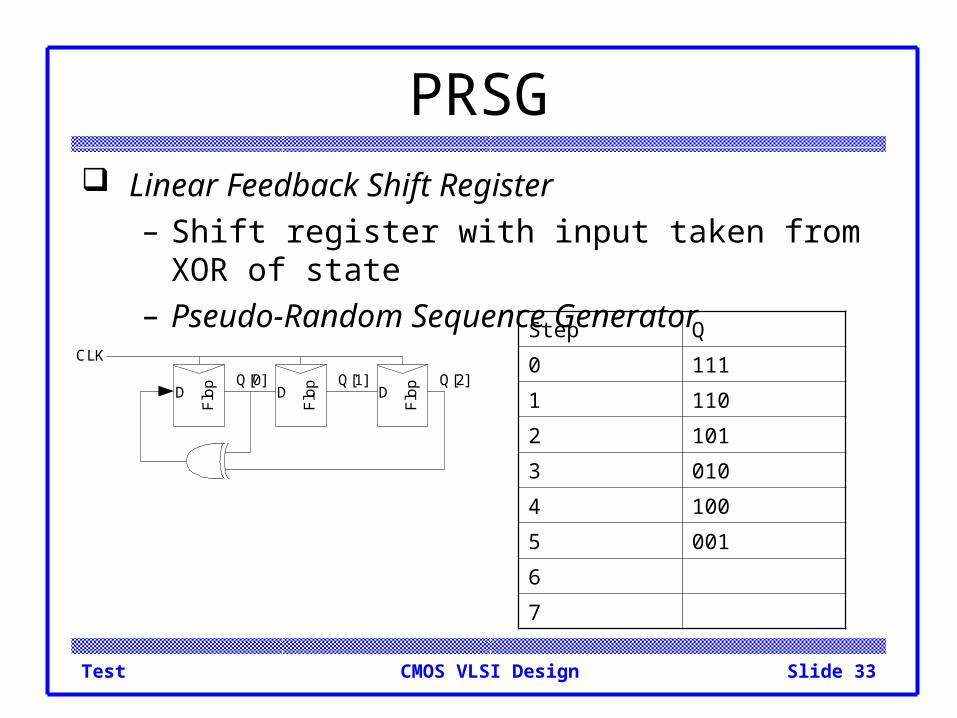
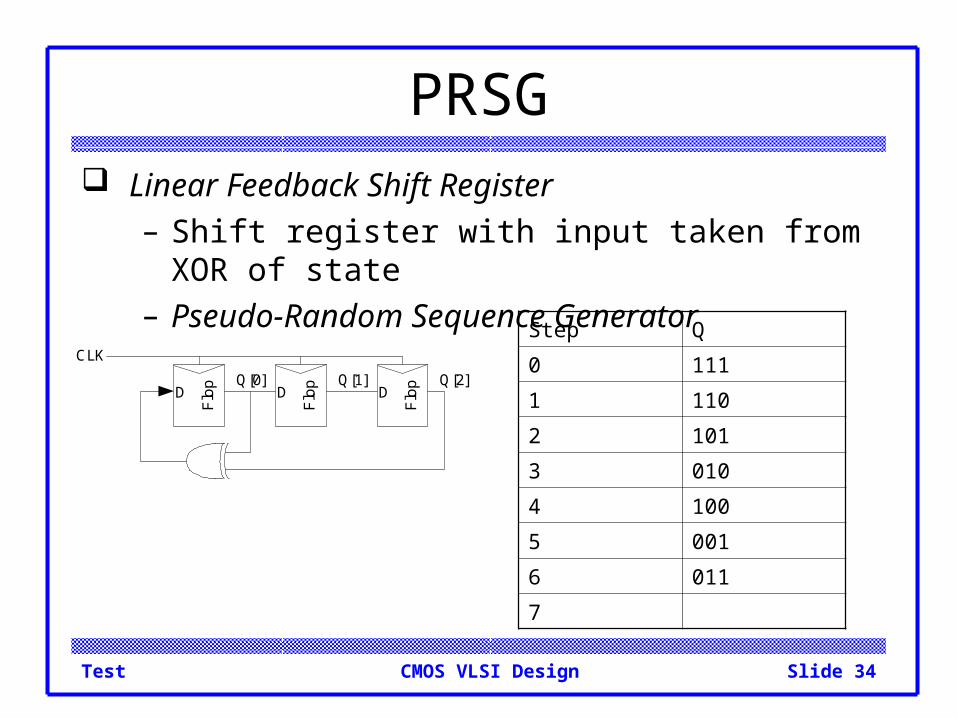
PRSG Linear Feedback Shift Register
– Shift register with input taken from XOR of state– Pseudo-Random Sequence Generator
Flo
p
Flo
p
Flo
pQ[0] Q[1] Q[2]
CLK
D D D
Step Q
0 111
1
2
3
4
5
6
7

Test Slide 29CMOS VLSI Design
PRSG Linear Feedback Shift Register
– Shift register with input taken from XOR of state– Pseudo-Random Sequence Generator
Flo
p
Flo
p
Flo
pQ[0] Q[1] Q[2]
CLK
D D D
Step Q
0 111
1 110
2
3
4
5
6
7

Test Slide 30CMOS VLSI Design
PRSG Linear Feedback Shift Register
– Shift register with input taken from XOR of state– Pseudo-Random Sequence Generator
Flo
p
Flo
p
Flo
pQ[0] Q[1] Q[2]
CLK
D D D
Step Q
0 111
1 110
2 101
3
4
5
6
7
Test Slide 31CMOS VLSI Design
PRSG Linear Feedback Shift Register
– Shift register with input taken from XOR of state– Pseudo-Random Sequence Generator
Flo
p
Flo
p
Flo
pQ[0] Q[1] Q[2]
CLK
D D D
Step Q
0 111
1 110
2 101
3 010
4
5
6
7

Test Slide 32CMOS VLSI Design
PRSG Linear Feedback Shift Register
– Shift register with input taken from XOR of state– Pseudo-Random Sequence Generator
Flo
p
Flo
p
Flo
pQ[0] Q[1] Q[2]
CLK
D D D
Step Q
0 111
1 110
2 101
3 010
4 100
5
6
7
Test Slide 33CMOS VLSI Design
PRSG Linear Feedback Shift Register
– Shift register with input taken from XOR of state– Pseudo-Random Sequence Generator
Flo
p
Flo
p
Flo
pQ[0] Q[1] Q[2]
CLK
D D D
Step Q
0 111
1 110
2 101
3 010
4 100
5 001
6
7
Test Slide 34CMOS VLSI Design
PRSG Linear Feedback Shift Register
– Shift register with input taken from XOR of state– Pseudo-Random Sequence Generator
Flo
p
Flo
p
Flo
pQ[0] Q[1] Q[2]
CLK
D D D
Step Q
0 111
1 110
2 101
3 010
4 100
5 001
6 011
7

Test Slide 35CMOS VLSI Design
PRSG Linear Feedback Shift Register
– Shift register with input taken from XOR of state– Pseudo-Random Sequence Generator
Flo
p
Flo
p
Flo
pQ[0] Q[1] Q[2]
CLK
D D D
Step Q
0 111
1 110
2 101
3 010
4 100
5 001
6 011
7 111 (repeats)
Test Slide 36CMOS VLSI Design
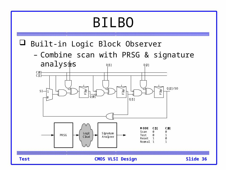
BILBO Built-in Logic Block Observer
– Combine scan with PRSG & signature analysis
MODE C[1] C[0]Scan 0 0Test 0 1Reset 1 0Normal 1 1
Flo
p
Flo
p
Flo
p
1
0
D[0] D[1] D[2]
Q[0]Q[1]
Q[2] / SOSI
C[1]C[0]
PRSGLogicCloud
SignatureAnalyzer
Test Slide 37CMOS VLSI Design
Boundary Scan Testing boards is also difficult
– Need to verify solder joints are good• Drive a pin to 0, then to 1• Check that all connected pins get the values
Through-hold boards used “bed of nails” SMT and BGA boards cannot easily contact pins Build capability of observing and controlling pins into
each chip to make board test easier
Test Slide 38CMOS VLSI Design
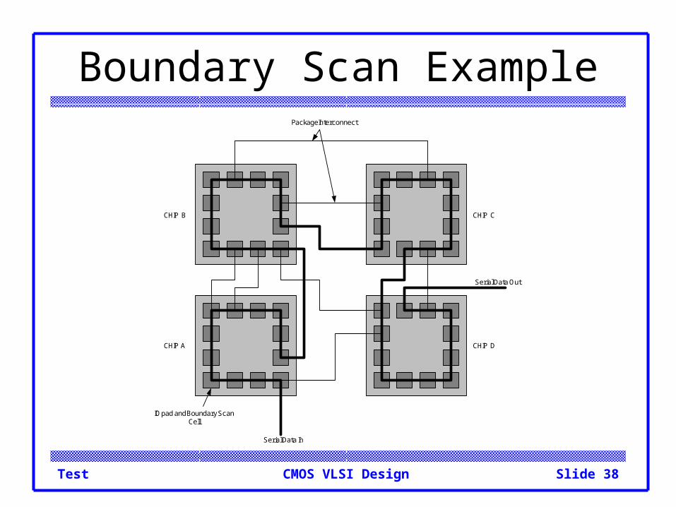
Boundary Scan Example
Serial Data In
Serial Data Out
Package Interconnect
IO pad and Boundary ScanCell
CHIP A
CHIP B CHIP C
CHIP D

Test Slide 39CMOS VLSI Design
Boundary Scan Interface Boundary scan is accessed through five pins
– TCK: test clock– TMS: test mode select– TDI: test data in– TDO: test data out– TRST*: test reset (optional)
Chips with internal scan chains can access the chains through boundary scan for unified test strategy.
Test Slide 40CMOS VLSI Design
Summary Think about testing from the beginning
– Simulate as you go– Plan for test after fabrication
“If you don’t test it, it won’t work! (Guaranteed)”