Embed Size (px)
Citation preview
Introduction toCMOS VLSI
Design
Lecture 19: Nonideal Transistors
David Harris
Harvey Mudd College
Spring 2007
19: Nonideal Transistors Slide 2CMOS VLSI Design
Outline Transistor I-V Review Nonideal Transistor Behavior
– Velocity Saturation– Channel Length Modulation– Body Effect– Leakage– Temperature Sensitivity
Process and Environmental Variations– Process Corners
19: Nonideal Transistors Slide 3CMOS VLSI Design
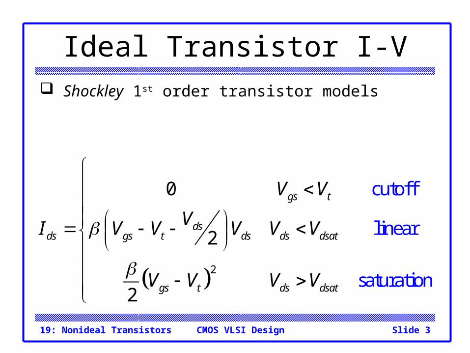
Ideal Transistor I-V Shockley 1st order transistor models
2
cutoff
linear
saturatio
0
2
2n
gs t
dsds gs t ds ds dsat
gs t ds dsat
V V
VI V V V V V
V V V V
19: Nonideal Transistors Slide 4CMOS VLSI Design
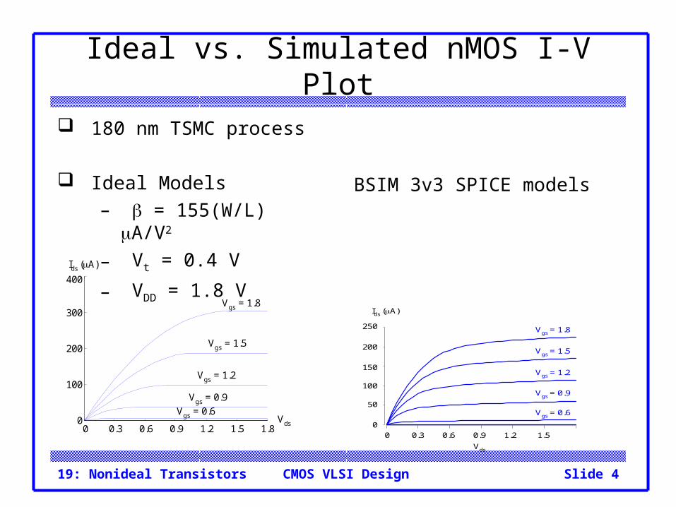
Ideal vs. Simulated nMOS I-V Plot
180 nm TSMC process
Ideal Models– = 155(W/L) A/V2
– Vt = 0.4 V
– VDD = 1.8 VIds (A)
Vds0 0.3 0.6 0.9 1.2 1.5 1.8
100
200
300
400
Vgs = 0.6
Vgs = 0.9
Vgs = 1.2
Vgs = 1.5
Vgs = 1.8
0
Vds
0 0.3 0.6 0.9 1.2 1.5
Vgs = 1.8
Ids (A)
0
50
100
150
200
250
Vgs = 1.5
Vgs = 1.2
Vgs = 0.9
Vgs = 0.6
BSIM 3v3 SPICE models
19: Nonideal Transistors Slide 5CMOS VLSI Design
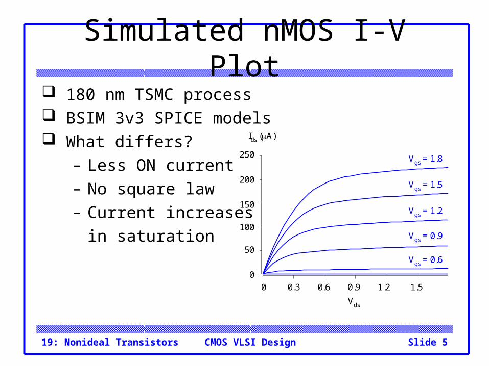
Simulated nMOS I-V Plot 180 nm TSMC process BSIM 3v3 SPICE models What differs?
– Less ON current– No square law– Current increases
in saturation
Vds
0 0.3 0.6 0.9 1.2 1.5
Vgs = 1.8
Ids (A)
0
50
100
150
200
250
Vgs = 1.5
Vgs = 1.2
Vgs = 0.9
Vgs = 0.6
19: Nonideal Transistors Slide 6CMOS VLSI Design
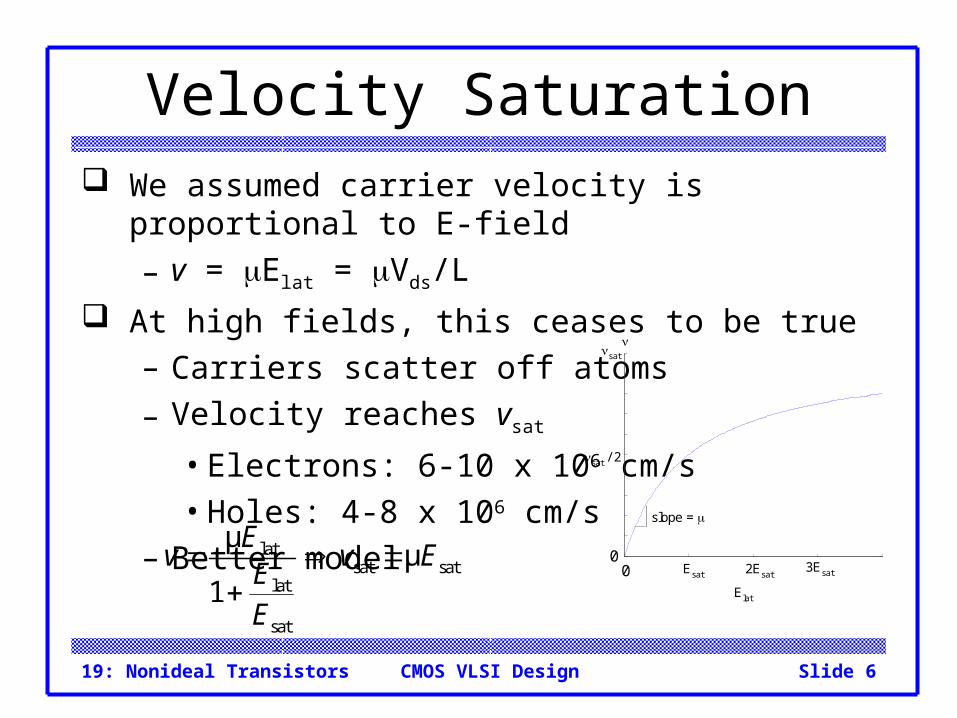
Velocity Saturation We assumed carrier velocity is proportional to E-field
– v = Elat = Vds/L
At high fields, this ceases to be true– Carriers scatter off atoms
– Velocity reaches vsat
• Electrons: 6-10 x 106 cm/s• Holes: 4-8 x 106 cm/s
– Better modelEsat0
0
slope =
Elat
2Esat3Esat
sat
sat / 2
latsat sat
lat
sat
μμ
1
Ev v E
EE
19: Nonideal Transistors Slide 7CMOS VLSI Design
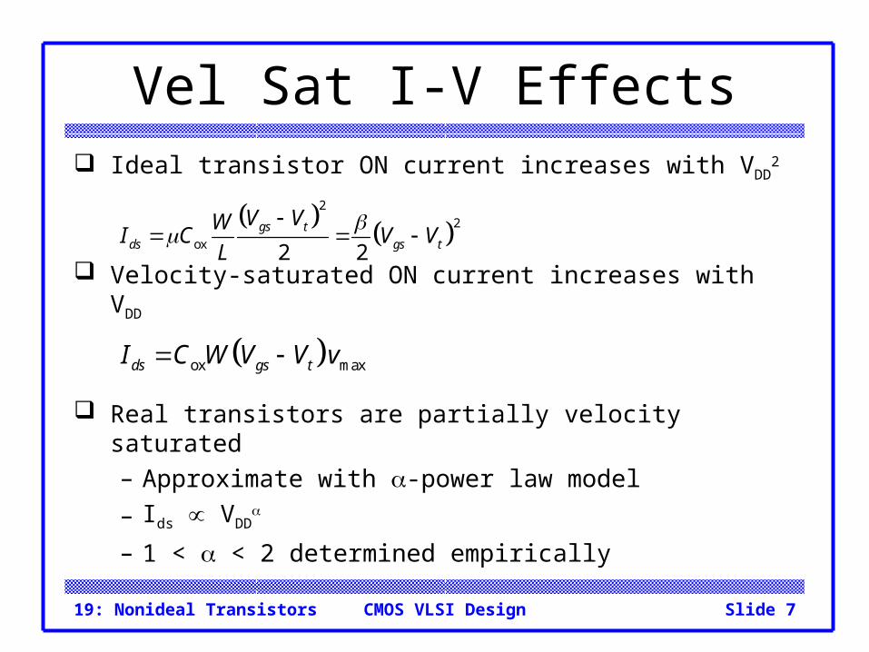
Vel Sat I-V Effects Ideal transistor ON current increases with VDD
2
Velocity-saturated ON current increases with VDD
Real transistors are partially velocity saturated– Approximate with -power law model
– Ids VDD
– 1 < < 2 determined empirically
2
2
ox 2 2gs t
ds gs t
V VWI C V V
L
ox maxds gs tI C W V V v
19: Nonideal Transistors Slide 8CMOS VLSI Design
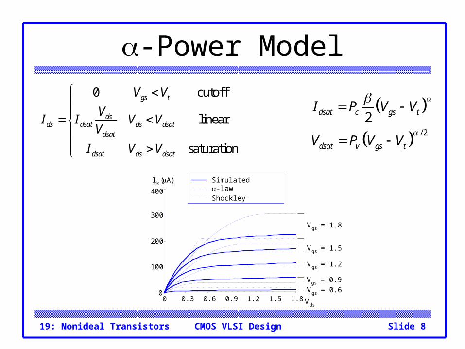
-Power Model
Ids (A)
Vds0 0.3 0.6 0.9 1.2 1.5 1.8
100
200
300
400
Vgs = 0.6
Vgs = 0.9
Vgs = 1.2
Vgs = 1.5
Vgs = 1.8
0
-lawSimulated
Shockley
0 cutoff
linear
saturation
gs t
dsds dsat ds dsat
dsat
dsat ds dsat
V V
VI I V V
V
I V V
/ 2
2dsat c gs t
dsat v gs t
I P V V
V P V V
19: Nonideal Transistors Slide 9CMOS VLSI Design
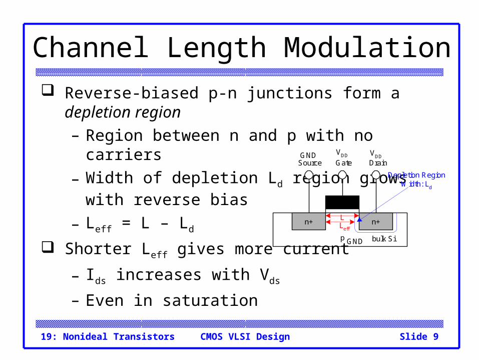
Channel Length Modulation Reverse-biased p-n junctions form a depletion region
– Region between n and p with no carriers
– Width of depletion Ld region grows with reverse bias
– Leff = L – Ld
Shorter Leff gives more current
– Ids increases with Vds
– Even in saturation
n+
p
GateSource Drain
bulk Si
n+
VDDGND VDD
GND
LLeff
Depletion RegionWidth: Ld
19: Nonideal Transistors Slide 10CMOS VLSI Design
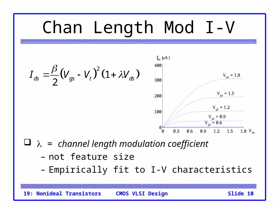
Chan Length Mod I-V
= channel length modulation coefficient– not feature size– Empirically fit to I-V characteristics
21
2ds gs t dsI V V V
Ids (A)
Vds0 0.3 0.6 0.9 1.2 1.5 1.8
100
200
300
400
Vgs = 0.6Vgs = 0.9
Vgs = 1.2
Vgs = 1.5
Vgs = 1.8
0
19: Nonideal Transistors Slide 11CMOS VLSI Design
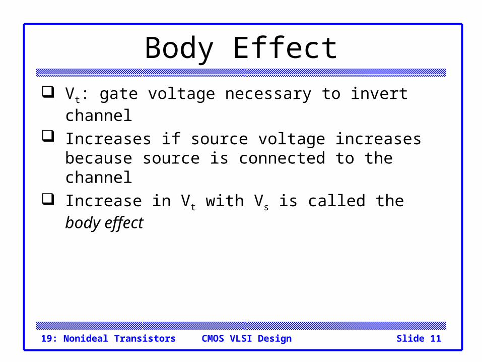
Body Effect Vt: gate voltage necessary to invert channel
Increases if source voltage increases because source is connected to the channel
Increase in Vt with Vs is called the body effect
19: Nonideal Transistors Slide 12CMOS VLSI Design
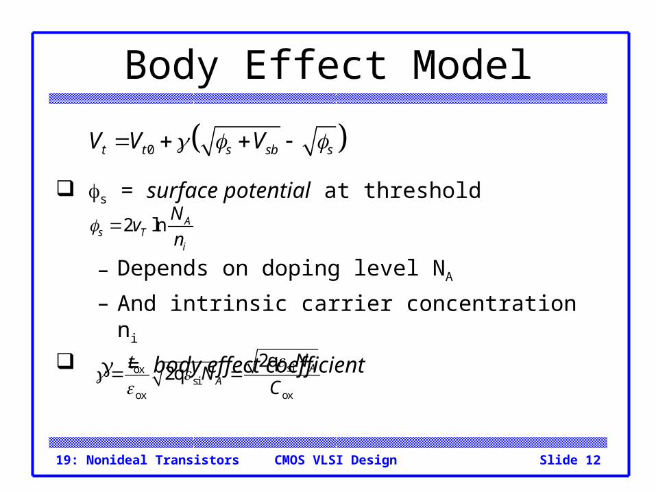
Body Effect Model
s = surface potential at threshold
– Depends on doping level NA
– And intrinsic carrier concentration ni
= body effect coefficient
0t t s sb sV V V
2 ln As T
i
Nv
n
sioxsi
ox ox
2q2q A
A
NtN
C
19: Nonideal Transistors Slide 13CMOS VLSI Design
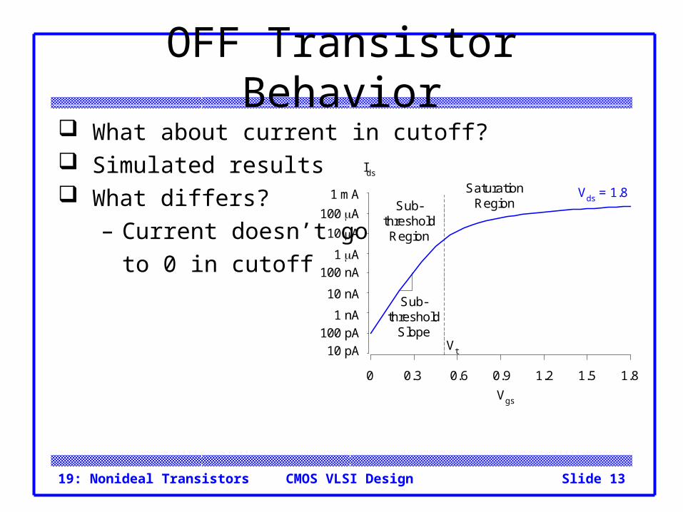
OFF Transistor Behavior What about current in cutoff? Simulated results What differs?
– Current doesn’t go
to 0 in cutoff
Vt
Sub-threshold
Slope
Sub-thresholdRegion
SaturationRegion
Vds = 1.8
Ids
Vgs
0 0.3 0.6 0.9 1.2 1.5 1.8
10 pA
100 pA
1 nA
10 nA
100 nA
1 A
10 A
100 A
1 mA
19: Nonideal Transistors Slide 14CMOS VLSI Design
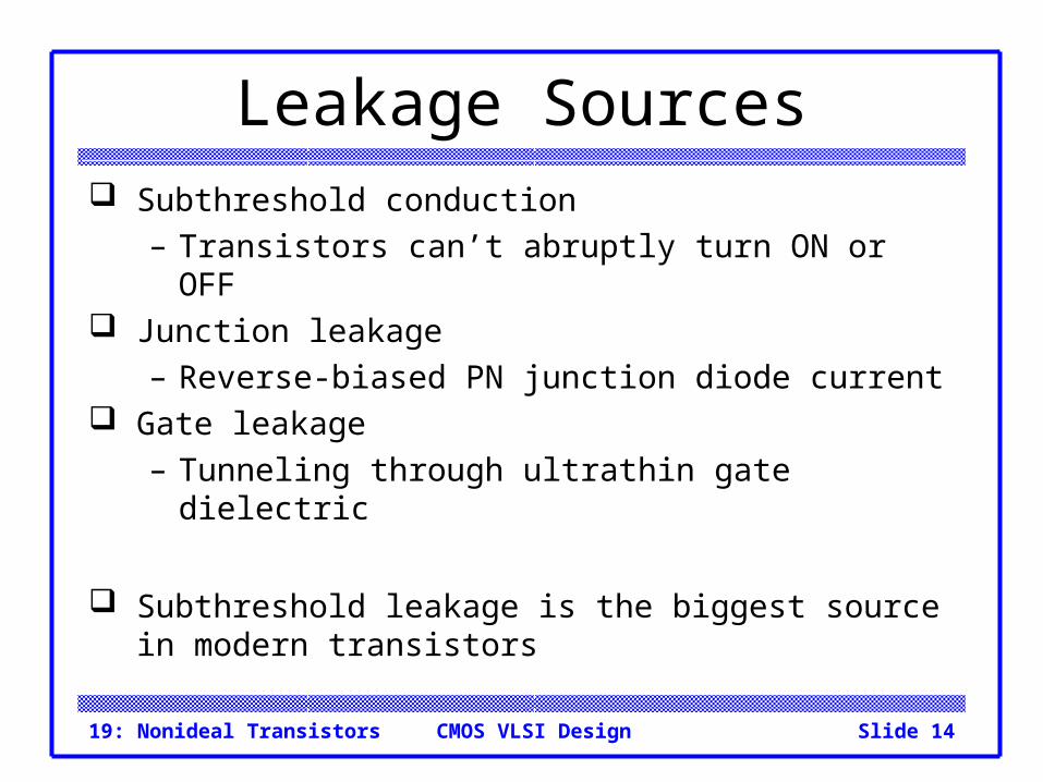
Leakage Sources Subthreshold conduction
– Transistors can’t abruptly turn ON or OFF Junction leakage
– Reverse-biased PN junction diode current Gate leakage
– Tunneling through ultrathin gate dielectric
Subthreshold leakage is the biggest source in modern transistors
19: Nonideal Transistors Slide 15CMOS VLSI Design
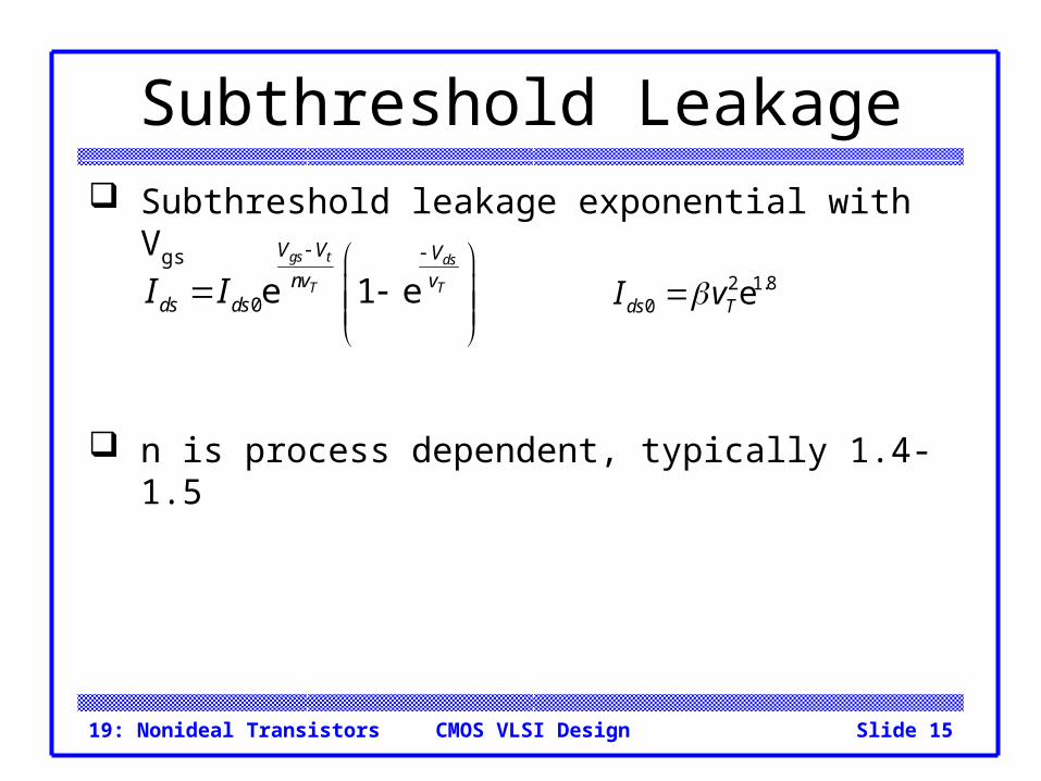
Subthreshold Leakage Subthreshold leakage exponential with Vgs
n is process dependent, typically 1.4-1.5
0e 1 egs t ds
T T
V V V
nv vds dsI I
2 1.80 eds TI v
19: Nonideal Transistors Slide 16CMOS VLSI Design
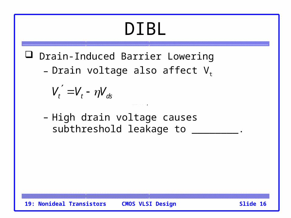
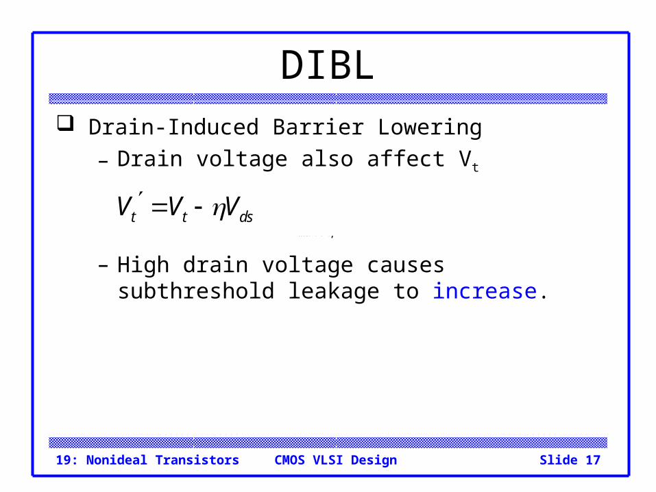
DIBL Drain-Induced Barrier Lowering
– Drain voltage also affect Vt
– High drain voltage causes subthreshold leakage to ________.
ttdsVVVt t dsV V V
19: Nonideal Transistors Slide 17CMOS VLSI Design
DIBL Drain-Induced Barrier Lowering
– Drain voltage also affect Vt
– High drain voltage causes subthreshold leakage to increase.
ttdsVVVt t dsV V V
19: Nonideal Transistors Slide 18CMOS VLSI Design
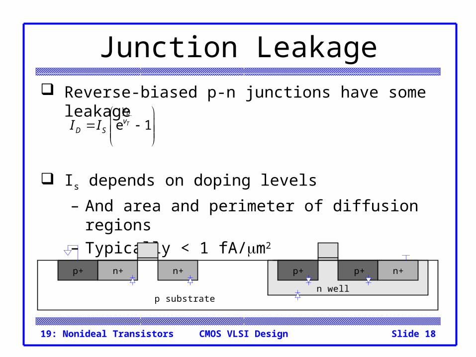
Junction Leakage Reverse-biased p-n junctions have some leakage
Is depends on doping levels
– And area and perimeter of diffusion regions– Typically < 1 fA/m2
e 1D
T
V
vD SI I
n well
n+n+ n+p+p+p+
p substrate
19: Nonideal Transistors Slide 19CMOS VLSI Design
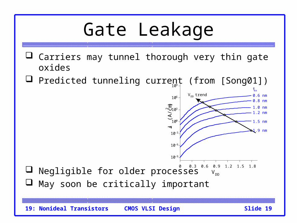
Gate Leakage Carriers may tunnel thorough very thin gate oxides Predicted tunneling current (from [Song01])
Negligible for older processes May soon be critically important
VDD
0 0.3 0.6 0.9 1.2 1.5 1.8J G
(A
/cm2
)
10-9
10-6
10-3
100
103
106
109
tox
0.6 nm0.8 nm
1.0 nm1.2 nm
1.5 nm
1.9 nm
VDD trend
19: Nonideal Transistors Slide 20CMOS VLSI Design
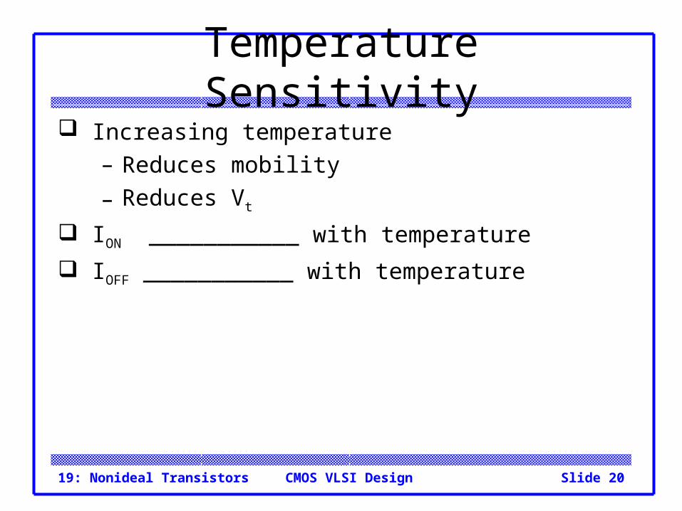
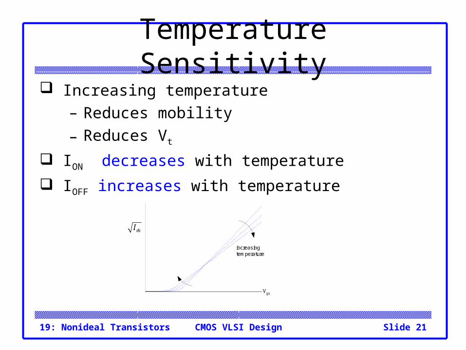
Temperature Sensitivity Increasing temperature
– Reduces mobility
– Reduces Vt
ION ___________ with temperature
IOFF ___________ with temperature
19: Nonideal Transistors Slide 21CMOS VLSI Design
Temperature Sensitivity Increasing temperature
– Reduces mobility
– Reduces Vt
ION decreases with temperature
IOFF increases with temperature
Vgs
dsI
increasingtemperature
19: Nonideal Transistors Slide 22CMOS VLSI Design
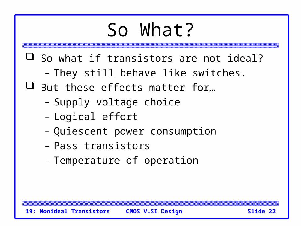
So What? So what if transistors are not ideal?
– They still behave like switches. But these effects matter for…
– Supply voltage choice– Logical effort– Quiescent power consumption– Pass transistors– Temperature of operation
19: Nonideal Transistors Slide 23CMOS VLSI Design
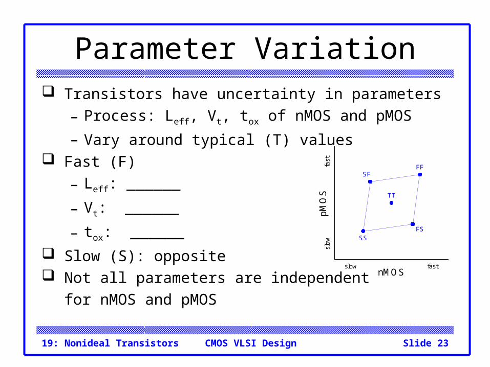
Parameter Variation Transistors have uncertainty in parameters
– Process: Leff, Vt, tox of nMOS and pMOS
– Vary around typical (T) values Fast (F)
– Leff: ______
– Vt: ______
– tox: ______
Slow (S): opposite Not all parameters are independent
for nMOS and pMOS
nMOS
pM
OS
fastslow
slow
fast
TT
FF
SS
FS
SF
19: Nonideal Transistors Slide 24CMOS VLSI Design
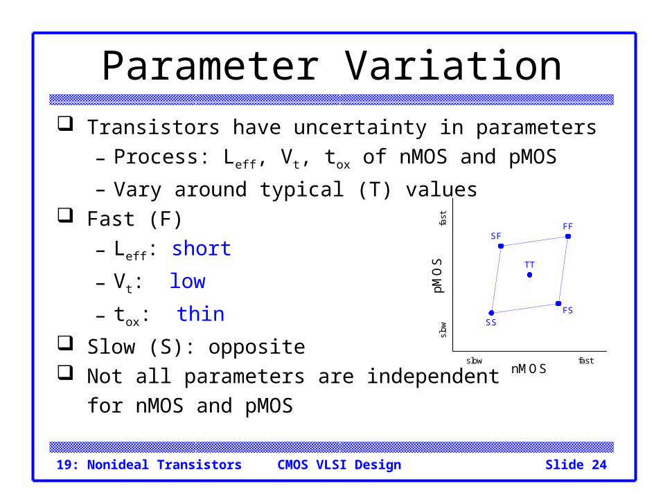
Parameter Variation Transistors have uncertainty in parameters
– Process: Leff, Vt, tox of nMOS and pMOS
– Vary around typical (T) values Fast (F)
– Leff: short
– Vt: low
– tox: thin
Slow (S): opposite Not all parameters are independent
for nMOS and pMOS
nMOS
pM
OS
fastslow
slow
fast
TT
FF
SS
FS
SF
19: Nonideal Transistors Slide 25CMOS VLSI Design
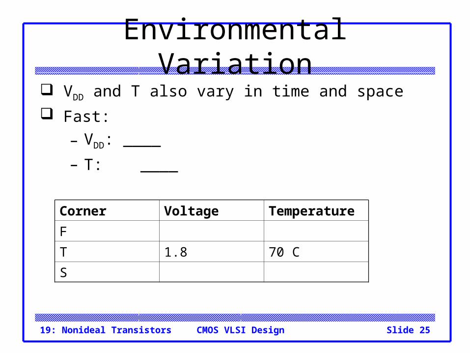
Environmental Variation VDD and T also vary in time and space
Fast:
– VDD: ____
– T: ____
Corner Voltage Temperature
F
T 1.8 70 C
S
19: Nonideal Transistors Slide 26CMOS VLSI Design
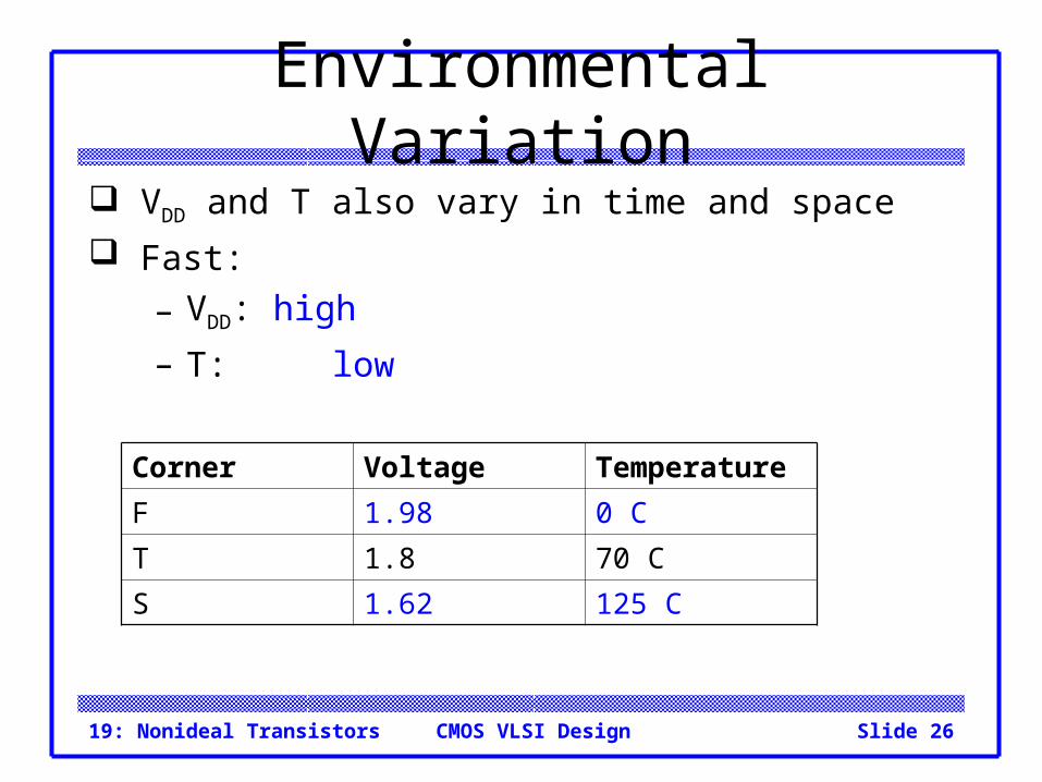
Environmental Variation VDD and T also vary in time and space
Fast:
– VDD: high
– T: low
Corner Voltage Temperature
F 1.98 0 C
T 1.8 70 C
S 1.62 125 C
19: Nonideal Transistors Slide 27CMOS VLSI Design
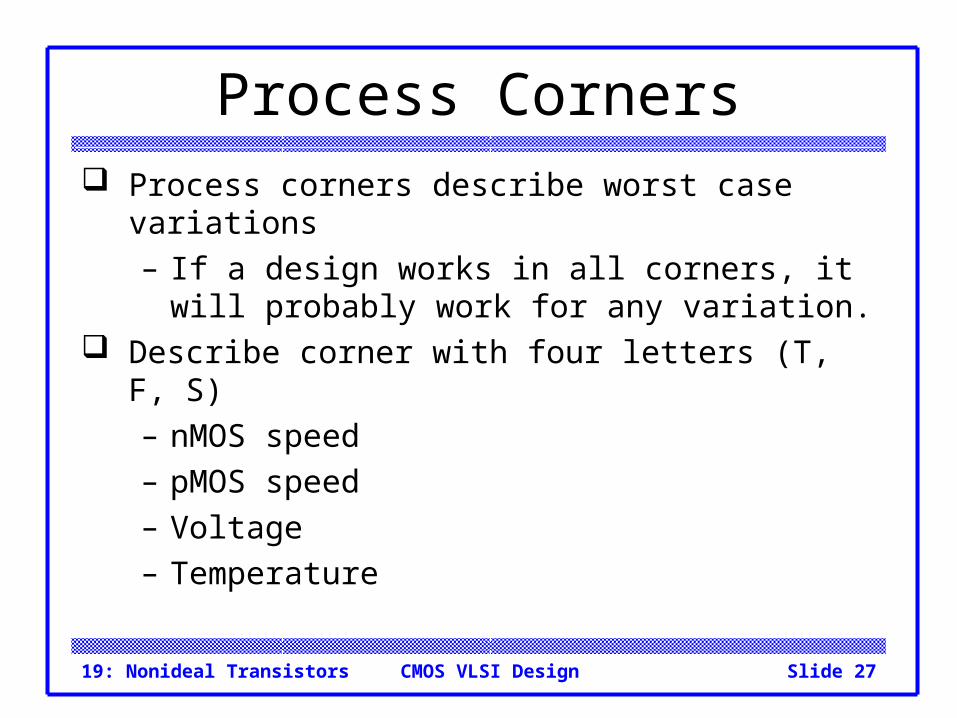
Process Corners Process corners describe worst case variations
– If a design works in all corners, it will probably work for any variation.
Describe corner with four letters (T, F, S)– nMOS speed– pMOS speed– Voltage– Temperature

19: Nonideal Transistors Slide 28CMOS VLSI Design
Important Corners Some critical simulation corners include
Purpose nMOS pMOS VDD Temp
Cycle time
Power
Subthrehold
leakage
Pseudo-nMOS
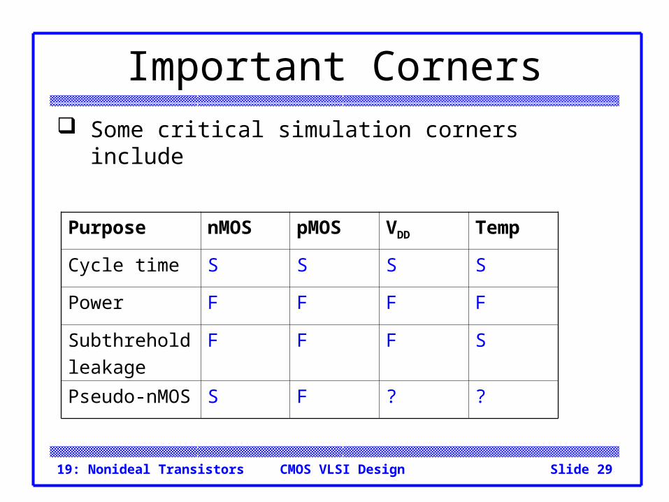
19: Nonideal Transistors Slide 29CMOS VLSI Design
Important Corners Some critical simulation corners include
Purpose nMOS pMOS VDD Temp
Cycle time S S S S
Power F F F F
Subthrehold
leakage
F F F S
Pseudo-nMOS S F ? ?