Embed Size (px)
Citation preview
18
CO
LU
MN
SUMMARY — Board-level simulation reduces costs by identifying potential problems at the conceptual stage, so that they can easily be avoided, and then catching any further issues, during the design process, eliminating the potentially disastrous final stage changes.
High-speed digital multilayer boards can be designed to work right the first time, with little additional effort, providing you follow a tried and proven process that results in a reli-able, manufacturable design that conforms to specifications and is produced on time and to budget.
Typically, a high-speed, computer-based de-sign takes three iterations to develop a working product. However, the product life cycle these days is very short, and therefore, time-to-mar-ket is of essence. One board iteration can cost more than $25K. And this is only in engineer-ing time and does not consider the cost of de-
laying the products’ market launch. This missed opportunity could cost hundreds of thousands of dollars.
If changes are made late in the design pro-cess, then it takes more time, people, material and therefore, money. The idea of board-level simulation is to identify issues early in the de-sign process and rectify them before they be-come a major problem.
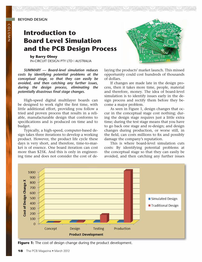
As seen in Figure 1, design changes that oc-cur in the conceptual stage cost nothing; dur-ing the design stage requires just a little extra time; during the test stage means that you have to go back one stage and re-design; and design changes during production, or worse still, in the field, can costs millions to fix and possibly damage the company’s reputation.
This is where board-level simulation cuts costs: By identifying potential problems at the conceptual stage so that they can easily be avoided, and then catching any further issues
Introduction to Board Level Simulation and the PCB Design Process
by Barry Olney IN-CIRCUIT DESIGN PTY LTD | AUSTRALIA
BEYOND DESIGN
Figure 1: The cost of design change during the product development.
20
during the design process, which eliminates the potentially disastrous final stage changes. Of course, we also need to keep our eye on the ball during the entire design process by catch-ing any small issue before it becomes a major problem.
Board level simulation and the design pro-cess cover the following:
1. Stackup planning 2. PDN planning 3. Design rules and DFM 4. Pre-layout simulation 5. Mixed analog digital technologies 6. Critical placement 7. Interactive placement and routing strategies 8. Critical routing 9. Post-layout simulation (already done)
I will be reviewing these topics in more de-tail over the coming months, but here are some initial factors to consider for each:
1. Stackup PlanningThe configuration of the PCB stackup de-
pends on many factors, but whatever the re-quirements, one should ensure that the follow-ing rules are followed in order to avoid a pos-sible debacle.
closely coupled to a reference plane, creating a clear return path and eliminating broadside crosstalk.
-ductance at high frequencies.
-tween the planes to reduce radiation.
an even number of layers, which prevents the PCB from warping during manufacture and re-flow.
-ber of different technologies.
It is not always possible to configure the stackup to have both tight coupling of the planes and tight coupling of the signal layers to the planes, as this depends on the number of layers and the available materials. Four- and six-layer boards typically have this issue. Fortu-
nately, the lower layer count boards are gener-ally used for designs below 100 MHz so the in-terplane capacitance may not be so important at these frequencies.
It is imperative that we plan the board stack-up from the beginning, ensuring that both sin-gle-ended and differential impedances conform to the technology requirements. And, be sure to ensure that the selected materials are available from our chosen fabrication shop — this step is regularly missed. Changing the stackup to-wards the end of the design process could mean changing trace widths and clearances to achieve the correct impedance, which could create a lot of unnecessary work.
At this stage we need to plan where the power planes will be in the stackup, considering that every signal layer needs to have a reference plane (either ground or power) adjacent to it in order to provide a clear return path.
2. PDN PlanningThe design of the power distribution net-
work (PDN) is also a very important part of the conceptual design process, ensuring that we have a stable power delivery system before we even start placing a chip on the board.
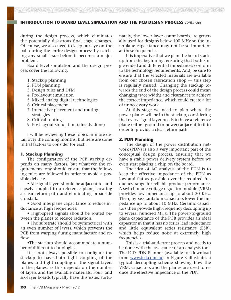
The idea of AC analysis of the PDN is to keep the effective impedance of the PDN as low and flat as possible over the required fre-quency range for reliable product performance. A switch mode voltage regulator module (VRM) provides low impedance up to about 30 KHz. Then, bypass tantalum capacitors lower the im-pedance up to about 10 MHz. Ceramic capaci-tors then provide high-frequency decoupling up to several hundred MHz. The power-to-ground plane capacitance of the PCB provides an ideal capacitor in that it has no series lead inductance and little equivalent series resistance (ESR), which helps reduce noise at extremely high frequencies.
This is a trial-and-error process and needs to be done with the assistance of an analysis tool. The ICD PDN Planner (available for download from www.icd.com.au) in Figure 3 illustrates a typical decoupling scheme showing how the VRM, capacitors and the planes are used to re-duce the effective impedance of the PDN.
INTRODUCTION TO BOARD LEVEL SIMULATION AND THE PCB DESIGN PROCESS continues
21
3. Design Rules and Design for Manufacturability (DFM)
Design rules should be set up and attached to critical nets in the schematic. This allows the engineer to transfer his desired intent, with re-gard to placement and routing, to the PCB de-signer without the information being lost in the process. One should keep in mind that if rules are modified in the PCB database then they need to be back-annotated to the schematic or they may be lost.
Design rules should be based on the man-ufacturer’s device specifications and the rel-evant industry documents and standards that are available. For instance, DDR2 specifications (JESD79-2E) can be downloaded from JEDEC. Also, there are design guides and design tech-nique documents available for download from Micron, Xilinx, Altera, etc., which are very helpful.
The IPC–2220 series of design documents, developed over the years by the industry, con-tain essential information for the design of SMT and mixed-signal multilayer boards and should be used to set up the basic design rules (www.ipc.org).
The technology rules are based on the mini-mum pitch of the BGA components employed and are basically the largest trace, clearance and via allowable whilst minimizing PCB fabrica-tion costs.
Once these rules have been established, cal-culate the stackup required for the desired char-acteristic impedance (Z
o) and the differential
impedance (Zdiff). These are typically Zo = 50
ohms and Zdiff = 100 ohms. The ICD Stackup Planner can be used for these calculations. Keep in mind that lower impedance will increase the dI/dt and dramatically increase the current drawn (not good for the PDN); higher imped-ance will emit more EMI and also make the de-sign more susceptible to outside interference. So, a good range of Z
o is 50 - 60 ohms.
Design for manufacturability (DFM) is the practice of designing board products that can be produced in a cost effective manner using existing manufacturing processes and equip-ment.
DFM is gaining more recognition as it be-comes clear that the cost reduction of printed circuit assemblies cannot be controlled by man-ufacturing engineers alone. The PCB designer
INTRODUCTION TO BOARD LEVEL SIMULATION AND THE PCB DESIGN PROCESS continues
Figure 2: The ICD PDN Planner illustrates a typical decoupling scheme for 1.8V DDR2.
22
now plays a critical role in cost saving and the DFM needs to be practiced throughout the entire design process. Again, identifying an issue too far into the process can cost time and money.
4. Pre-Layout SimulationPre-layout simulation allows the designer to
predict and eliminate signal integrity, crosstalk and EMC issues early in the design process. This is the most cost effective way to design a board with fewer iterations rather than starting with the post-layout simulation.
One can quickly simulate complex inter-connect scenarios including integrated circuits, transmission lines, connectors and passive components and identify which scenario is best suited to a particular design.
The value and placement of the series resis-tors and VTT pull-ups for data, address and com-mand nets depends on the distances between the loads, number of loads and the stackup of the board, and are best determined by simula-tion. The series terminator may not be required if a single memory chip is used and the trace length is short.
5. Mixed Analog and Digital TechnologiesIn the past, we have only had to deal with
mixed analog and digital technologies, but ra-dio frequency (RF) and analog mixed-signal (AMS) technologies, which serve the rapidly growing wireless communication market, are essential in today’s PCB design. A digital system is also an RF system with significant noise and therefore interference potential.
Digital technologies with different voltage levels can also cause interfere with each other. The technology being used has changed quite dramatically over the years, from TTL devices
(with high thresholds) to today’s high-speed Gb/s devices (with noise margins as low as 500mV). The trend is toward lower processor core voltages, which conserves power. But, re-ducing the core voltage also reduces maximum operating frequency and the level of acceptable crosstalk.
In analog circuits, external noise sources are usually the primary concern. However, in digital circuits, the internally generated noise sources are of major concern.
When planes are used to distribute power supplies, crosstalk (coupling) can occur through the ground return path for these signals. This is called common-mode impedance coupling. Es-sentially, a returning signal causes a ground potential rise due to the DC resistance of the plane. This problem can be very significant, es-pecially in analog circuitry when digital signals are present.
Although a single-point ground may be de-sirable in low-frequency analog circuits, it may be the primary source of noise coupling and emissions in a digital circuit. When mixed an-alog and digital circuits are used on the same PCB, the best approach, for grounding practices is to use one solid and common ground plane and ensure that the routing of the traces does not create crosstalk.
6. Critical PlacementTo obtain an excellent route completion rate
on a complex design, placement is extremely important. If the board is difficult to route, it may just be the result of poor placement.
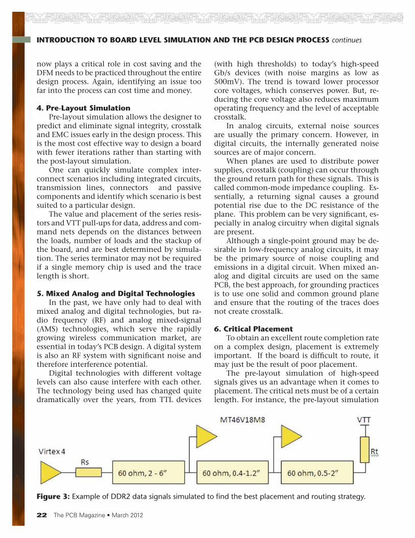
The pre-layout simulation of high-speed signals gives us an advantage when it comes to placement. The critical nets must be of a certain length. For instance, the pre-layout simulation
INTRODUCTION TO BOARD LEVEL SIMULATION AND THE PCB DESIGN PROCESS continues
Figure 3: Example of DDR2 data signals simulated to find the best placement and routing strategy.
23
might suggest that a balanced T section route of 1.5 inches on all address, command and control lines of our DDR2 memory would be the best approach, and that data and strobes be no more than 1.2 inches matched to within 25 mils. Ob-viously, this does not give us much room to play with, so the correct positioning of these devices initially is of paramount importance. Placing the processor in the centre of the board allows all signals to be fanned out and promotes star wiring which is best for high-speed signals.
7. Interactive Placement and Routing Strategies
When the engineer creates the schematic he does so in logical, functional blocks — and that is exactly the way we should place and route the PCB. Cross-probing between the schemat-ic and PCB database can be done in all major EDA packages and is recommended for design integrity.
For example, I often see PCB designers ran-domly placing resistors on the board. It is only a resistor — or is it? Well, that resistor could be a static pull-up that can be placed anywhere within reason or it could be a series terminator for a high-speed signal that needs to be placed within 200 mils of the driver. One should know the function of every component in order to make a valued decision with regard to effective placement, and cross-probing achieves this.
Critical placement should (of course) be done first. Then position the highest frequency components nearest the connectors and gradu-ate the placement from high to low speed de-vices, with the low frequency analog devices positioned farthest from the connectors in a corner. Highlight the components on the sche-matic and move them into position on the PCB, one by one, making sure that you have the en-tire functional block in the one area. This is a tedious process, but it is the only way to ensure the placement is optimum.
Interactive routing is done in much the same way. Firstly, cross-probe and select the critical signals from the schematic, fanout, and route on the board. Route in priority from the most critical to least critical nets. I often use the autorouter to finish off the non-critical nets, but this of course depends on the quality of the
autorouter. I certainly would not attempt this with a basic router.
8. Critical RoutingI previously mentioned that the pre-layout
simulation determines the placement of the critical components which in turn determines the critical routing topology. So, it is a simple process once you have the design methodology right, although at times one loses a bit of hair when tuning nets to length. Having so many matched-length signals on the size of a postage stamp is a daunting thought.
For DDR designs, differential clocks should be routed first, because all other signal lengths/delays are referenced to tClk, followed by data and strobe signals. Next, route the address, command and controls signals. It is best, al-though the pre-layout simulation has given us a routing strategy, to route a couple of each signal group first, then run the post-layout simulator to check the waveforms, skew and radiation on this sample group before continuing with the routing. The pre-layout simulation gives us a good heads-up, but the physical board simula-tion can be quite different in some cases.
9. Post-layout Board Level SimulationA preliminary batch mode simulation is ini-
tially completed on the design. Default IC char-acteristics, crosstalk of 150mV maximum and EMC to FCC, CISPR Class A and B are set up in the simulator. The batch mode simulation au-tomatically scans large numbers of nets on an entire PCB, flagging signal integrity, crosstalk and EMC hot spots.
The post-layout simulation analysis can then be prepared using supplied specifications. This is an extensive interactive board level sim-ulation which takes the analysis to the next level — simulating trouble spots identified by the batch analysis in order to further resolve the issues with greater accuracy.
Crosstalk is typically picked up on long, par-allel trace segments. These can be on the same layer, but may also be broadside coupled from the adjacent layer. It is for this reason that or-thogonal routing is recommended on adjacent layers (between planes) to minimize the cou-pling area.
INTRODUCTION TO BOARD LEVEL SIMULATION AND THE PCB DESIGN PROCESS continues
24
Flight times of the critical signals are then examined. One could compare the matched lengths of each signal, but delay will vary de-pending on the meander pattern.
Since all products must comply with strict electromagnetic compliancy (EMC) regulations, all critical high-speed signals should be simu-lated to determine the amount of expected ra-diation.
Board-level simulation is engaged too of-ten toward the end of the design cycle. Simu-lation should be done throughout the entire design process to ensure that the design is on track. A simulation service such as that provid-ed by In-Circuit Design can complement your design team. It will save you time, money and frustration, but more importantly, from an en-gineer’s or designer’s point of view, give you confidence in the performance and reliability of the product. PCB
References:1. Advanced Design for SMT – Barry Olney2. PCB Design Techniques for DDR, DDR2 &
DDR3 – Barry Olney
3. Design for EMC – PCD Magazine Jan 96, Barry Olney
4. The Perfect Stackup – Barry Olney5. Controlling the Beast – Barry Olney6. Matched Length Routing – Barry Olney7. High Speed Signal Propagation – Howard
Johnson8. Electromagnetic Compatibility Engineer-
ing – Henry Ott9. The ICD Stackup Planner and ICD
PDN Planner can be downloaded from www.icd.com.au.
Barry Olney is Managing Direc-tor of In-Circuit Design Pty Ltd. (ICD), Australia, a PCB Design Service Bureau and Board Level Simulation Specialist. Among others through the years, ICD was awarded “Top 2005 Asian Distributor Marketing and “Top
2005 Worldwide Distributor Marketing by Mentor Graphics, Board System Division. For more infor-mation, contact Barry Olney at +61 4123 14441 or email at [email protected].
to(SeSiotwa
INTRODUCTION TO BOARD LEVEL SIMULATION AND THE PCB DESIGN PROCESS continues
Miniaturization combined with ever increasing
functionality and enhanced reliability has become
part of our way of life, not least in the smartphone
sector. The Hermes Consortium’s task is to industrial-
ize new miniaturization technologies.
In spring 2008 AT&S brought together eleven re-
nowned European global players in one of the largest
ever EU-sponsored projects. The participants came
from different stages in the value chain in the automo-
tive, aeronautical and other industrial sectors.
Hermes goes far beyond what is currently pos-
sible in connectivity. Series production processes are
used to embed active components such as chips, as
well as passive components such as resistors and
capacitors in the interior of the PCBs. This creates
additional space on the circuit boards, and the im-
and extend the product’s useful life.
One of the Consortium’s main goals is to set
standards for the industry, and to generate advan-
tages over the competition in Asia. Industrial imple-
mentation of this technology opens up a wide range
of potential applications in medicine (including new
generations of hearing aids and pacemakers) and in
functional modules for GPS, WLAN, Bluetooth and
cameras. At the same time, AT&S is strengthening
its position with existing customers as an innovation
and technology leader, and is well placed to offer new
solutions.
ECP technology has been brought to market in
the course of the project following the successful con-
struction of the production line in Hinterberg. AT&S
picked up the Fast Forward Award 2011 for its ECP®
technology. In the next few years, the complexity in-
side and on the surface of the modules will continue
to grow, and the 3D capabilities of embedding tech-
nologies will pave the way for the next generation of
mobile electronic devices.
AT&S Leads Hermes
Consortium