Embed Size (px)
Citation preview
Introduction to Analog Electronics Fall 2016 ECE 3400
Professor Jennifer Hasler Course Project Guide
11/21/2016
Yusuf Ziya Kuriş
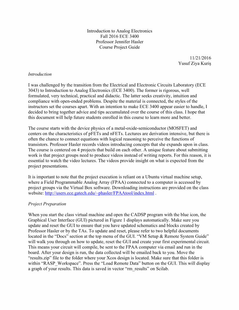
Introduction I was challenged by the transition from the Electrical and Electronic Circuits Laboratory (ECE 3043) to Introduction to Analog Electronics (ECE 3400). The former is rigorous, well formulated, very technical, practical and didactic. The latter seeks creativity, intuition and compliance with open-ended problems. Despite the material is connected, the styles of the instructors set the courses apart. With an intention to make ECE 3400 appear easier to handle, I decided to bring together advice and tips accumulated over the course of this class. I hope that this document will help future students enrolled in this course to learn more and better. The course starts with the device physics of a metal-oxide-semiconductor (MOSFET) and centers on the characteristics of pFETs and nFETs. Lectures are derivation intensive, but there is often the chance to connect equations with logical reasoning to perceive the functions of transistors. Professor Hasler records videos introducing concepts that she expands upon in class. The course is centered on 4 projects that build on each other. A unique feature about submitting work is that project groups need to produce videos instead of writing reports. For this reason, it is essential to watch the video lectures. The videos provide insight on what is expected from the project presentations. It is important to note that the project execution is reliant on a Ubuntu virtual machine setup, where a Field Programmable Analog Array (FPAA) connected to a computer is accessed by project groups via the Virtual Box software. Downloading instructions are provided on the class website: http://users.ece.gatech.edu/~phasler/FPAAtool/index.html . Project Preparation When you start the class virtual machine and open the CADSP program with the blue icon, the Graphical User Interface (GUI) pictured in Figure 1 displays automatically. Make sure you update and reset the GUI to ensure that you have updated schematics and blocks created by Professor Hasler or by the TAs. To update and reset, please refer to two helpful documents located in the “Docs” section at the top menu of the GUI. “VM Setup & Remote System Guide” will walk you through on how to update, reset the GUI and create your first experimental circuit. This means your circuit will compile, be sent to the FPAA computer via email and run in the board. After your design is run, the data collected will be emailed back to you. Move the “results.zip” file to the folder where your Xcos design is located. Make sure that this folder is within “RASP_Workspace”. Press the “Load Remote Data” button on the GUI. This will display a graph of your results. This data is saved in vector “rm_results” on Scilab.
Tip 1: Always enter “figure” before plotting any values. If not, the plot will appear in the GUI’s background!
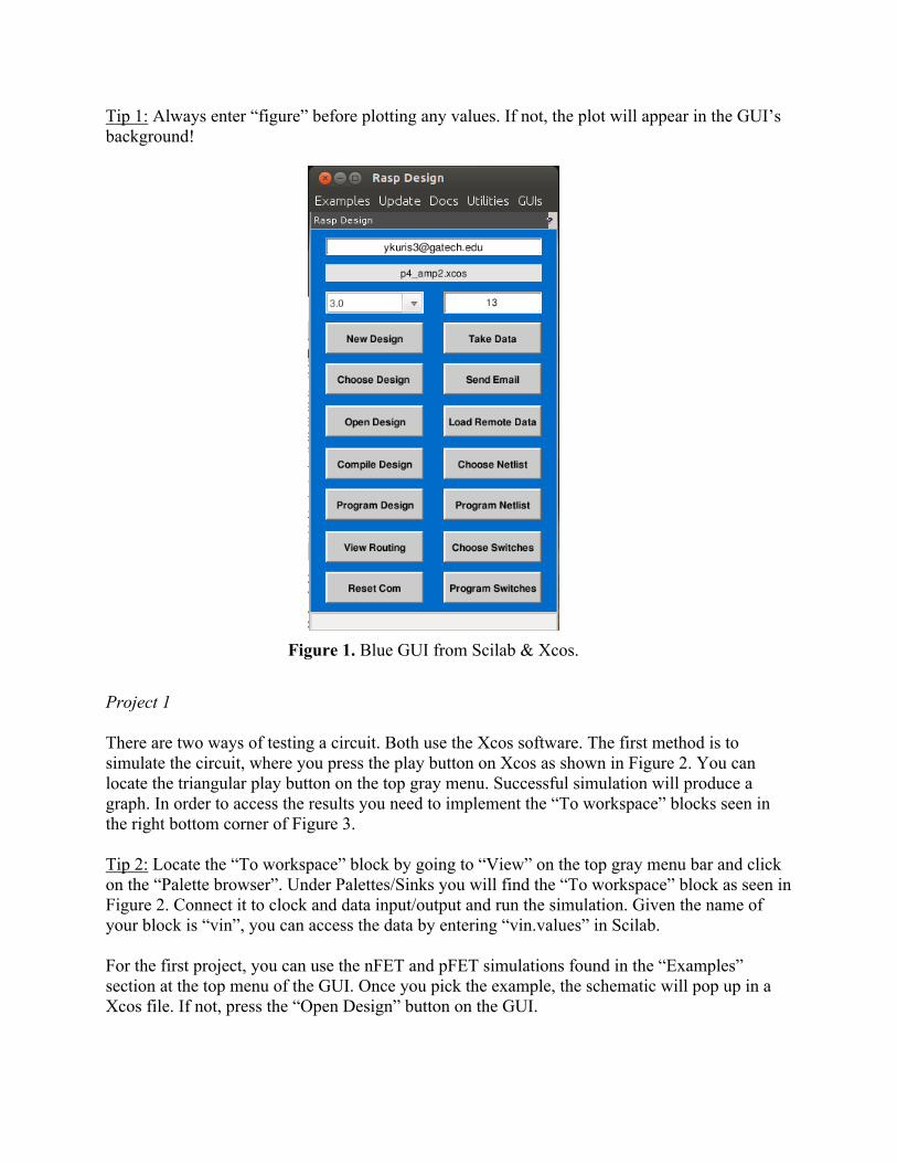
Project 1 There are two ways of testing a circuit. Both use the Xcos software. The first method is to simulate the circuit, where you press the play button on Xcos as shown in Figure 2. You can locate the triangular play button on the top gray menu. Successful simulation will produce a graph. In order to access the results you need to implement the “To workspace” blocks seen in the right bottom corner of Figure 3. Tip 2: Locate the “To workspace” block by going to “View” on the top gray menu bar and click on the “Palette browser”. Under Palettes/Sinks you will find the “To workspace” block as seen in Figure 2. Connect it to clock and data input/output and run the simulation. Given the name of your block is “vin”, you can access the data by entering “vin.values” in Scilab. For the first project, you can use the nFET and pFET simulations found in the “Examples” section at the top menu of the GUI. Once you pick the example, the schematic will pop up in a Xcos file. If not, press the “Open Design” button on the GUI.
Figure 1. Blue GUI from Scilab & Xcos.
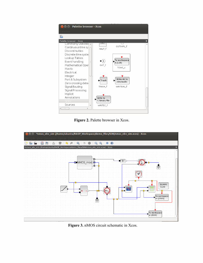
Figure 3. nMOS circuit schematic in Xcos.
Figure 2. Palette browser in Xcos.
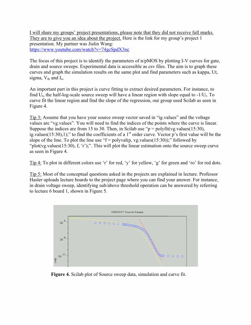
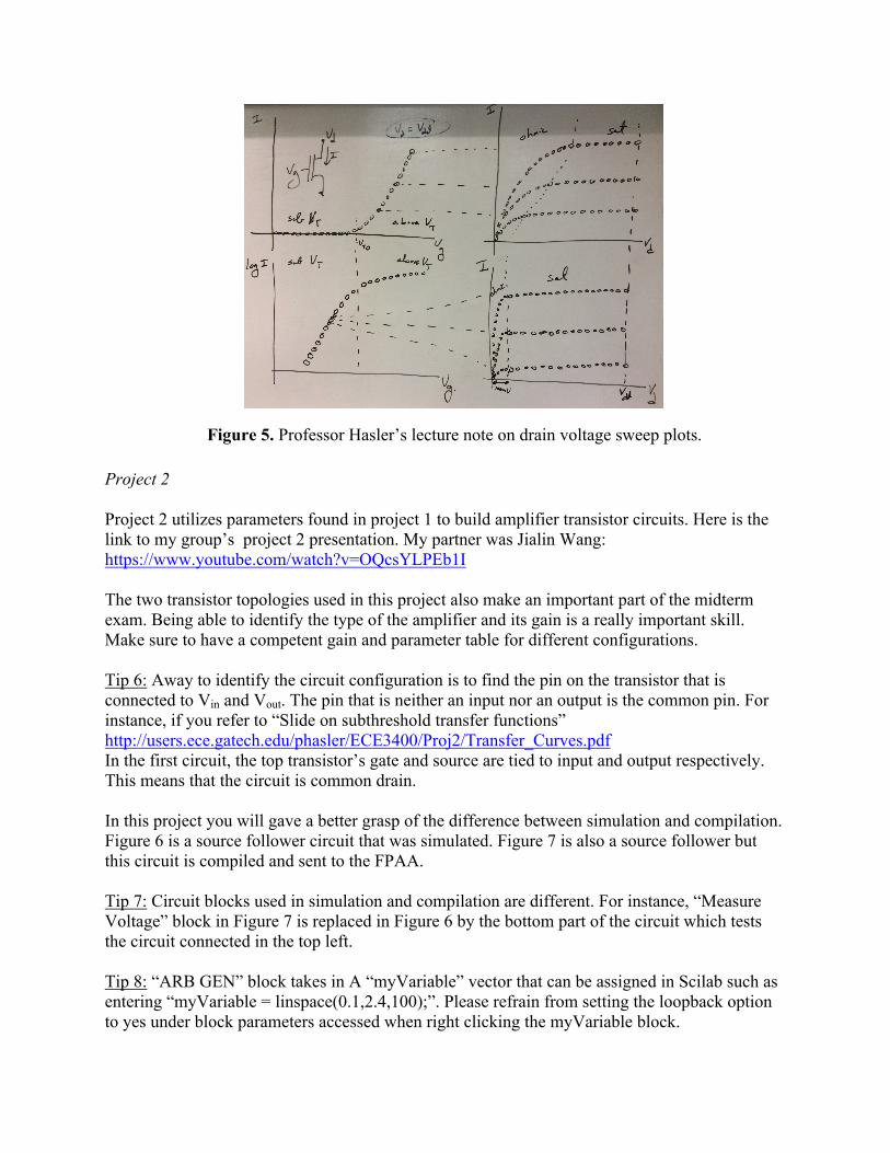
I will share my groups’ project presentations, please note that they did not receive full marks. They are to give you an idea about the project. Here is the link for my group’s project 1 presentation. My partner was Jialin Wang: https://www.youtube.com/watch?v=74gcSpdX3nc The focus of this project is to identify the parameters of n/pMOS by plotting I-V curves for gate, drain and source sweeps. Experimental data is accessible as csv files. The aim is to graph these curves and graph the simulation results on the same plot and find parameters such as kappa, Ut, sigma, Vth and Io. An important part in this project is curve fitting to extract desired parameters. For instance, to find Ut, the half-log-scale source sweep will have a linear region with slope equal to -1/Ut. To curve fit the linear region and find the slope of the regression, our group used Scilab as seen in Figure 4. Tip 3: Assume that you have your source sweep vector saved in “ig.values” and the voltage values are “vg.values”. You will need to find the indices of the points where the curve is linear. Suppose the indices are from 15 to 30. Then, in Scilab use “p = polyfit(vg.values(15:30), ig.values(15:30),1);” to find the coefficients of a 1st order curve. Vector p’s first value will be the slope of the line. To plot the line use “f = polyval(p, vg.values(15:30));” followed by “plot(vg.values(15:30), f, ‘r’);”. This will plot the linear estimation onto the source sweep curve as seen in Figure 4. Tip 4: To plot in different colors use ‘r’ for red, ‘y’ for yellow, ‘g’ for green and ‘ro’ for red dots. Tip 5: Most of the conceptual questions asked in the projects are explained in lecture. Professor Hasler uploads lecture boards to the project page where you can find your answer. For instance, in drain voltage sweep, identifying sub/above threshold operation can be answered by referring to lecture 6 board 1, shown in Figure 5.
Figure 4. Scilab plot of Source sweep data, simulation and curve fit.
Project 2 Project 2 utilizes parameters found in project 1 to build amplifier transistor circuits. Here is the link to my group’s project 2 presentation. My partner was Jialin Wang: https://www.youtube.com/watch?v=OQcsYLPEb1I The two transistor topologies used in this project also make an important part of the midterm exam. Being able to identify the type of the amplifier and its gain is a really important skill. Make sure to have a competent gain and parameter table for different configurations. Tip 6: Away to identify the circuit configuration is to find the pin on the transistor that is connected to Vin and Vout. The pin that is neither an input nor an output is the common pin. For instance, if you refer to “Slide on subthreshold transfer functions” http://users.ece.gatech.edu/phasler/ECE3400/Proj2/Transfer_Curves.pdf In the first circuit, the top transistor’s gate and source are tied to input and output respectively. This means that the circuit is common drain. In this project you will gave a better grasp of the difference between simulation and compilation. Figure 6 is a source follower circuit that was simulated. Figure 7 is also a source follower but this circuit is compiled and sent to the FPAA. Tip 7: Circuit blocks used in simulation and compilation are different. For instance, “Measure Voltage” block in Figure 7 is replaced in Figure 6 by the bottom part of the circuit which tests the circuit connected in the top left. Tip 8: “ARB GEN” block takes in A “myVariable” vector that can be assigned in Scilab such as entering “myVariable = linspace(0.1,2.4,100);”. Please refrain from setting the loopback option to yes under block parameters accessed when right clicking the myVariable block.
Figure 5. Professor Hasler’s lecture note on drain voltage sweep plots.
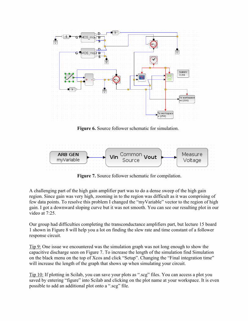
A challenging part of the high gain amplifier part was to do a dense sweep of the high gain region. Since gain was very high, zooming in to the region was difficult as it was comprising of few data points. To resolve this problem I changed the “myVariable” vector to the region of high gain. I got a downward sloping curve but it was not smooth. You can see our resulting plot in our video at 7:25. Our group had difficulties completing the transconductance amplifiers part, but lecture 15 board 1 shown in Figure 8 will help you a lot on finding the slew rate and time constant of a follower response circuit. Tip 9: One issue we encountered was the simulation graph was not long enough to show the capacitive discharge seen on Figure 7. To increase the length of the simulation find Simulation on the black menu on the top of Xcos and click “Setup”. Changing the “Final integration time” will increase the length of the graph that shows up when simulating your circuit. Tip 10: If plotting in Scilab, you can save your plots as “.scg” files. You can access a plot you saved by entering “figure” into Scilab and clicking on the plot name at your workspace. It is even possible to add an additional plot onto a “.scg” file.
Figure 6. Source follower schematic for simulation.
Figure 7. Source follower schematic for compilation.
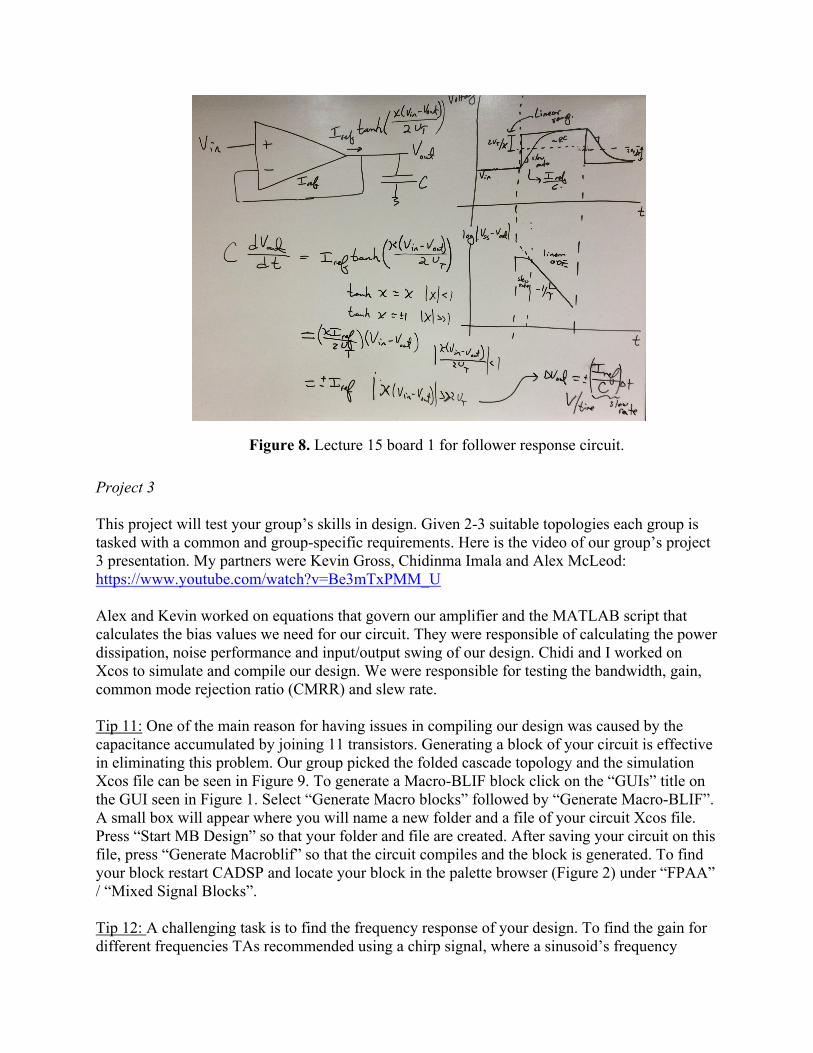
Project 3 This project will test your group’s skills in design. Given 2-3 suitable topologies each group is tasked with a common and group-specific requirements. Here is the video of our group’s project 3 presentation. My partners were Kevin Gross, Chidinma Imala and Alex McLeod: https://www.youtube.com/watch?v=Be3mTxPMM_U Alex and Kevin worked on equations that govern our amplifier and the MATLAB script that calculates the bias values we need for our circuit. They were responsible of calculating the power dissipation, noise performance and input/output swing of our design. Chidi and I worked on Xcos to simulate and compile our design. We were responsible for testing the bandwidth, gain, common mode rejection ratio (CMRR) and slew rate. Tip 11: One of the main reason for having issues in compiling our design was caused by the capacitance accumulated by joining 11 transistors. Generating a block of your circuit is effective in eliminating this problem. Our group picked the folded cascade topology and the simulation Xcos file can be seen in Figure 9. To generate a Macro-BLIF block click on the “GUIs” title on the GUI seen in Figure 1. Select “Generate Macro blocks” followed by “Generate Macro-BLIF”. A small box will appear where you will name a new folder and a file of your circuit Xcos file. Press “Start MB Design” so that your folder and file are created. After saving your circuit on this file, press “Generate Macroblif” so that the circuit compiles and the block is generated. To find your block restart CADSP and locate your block in the palette browser (Figure 2) under “FPAA” / “Mixed Signal Blocks”. Tip 12: A challenging task is to find the frequency response of your design. To find the gain for different frequencies TAs recommended using a chirp signal, where a sinusoid’s frequency
Figure 8. Lecture 15 board 1 for follower response circuit.
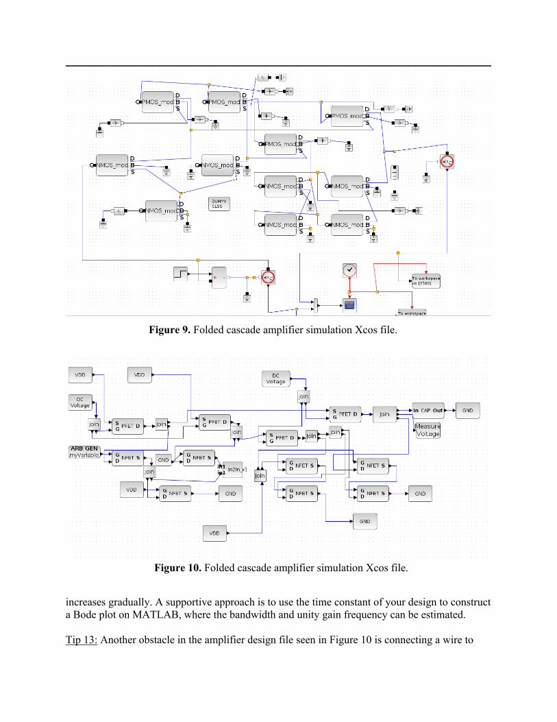
increases gradually. A supportive approach is to use the time constant of your design to construct a Bode plot on MATLAB, where the bandwidth and unity gain frequency can be estimated. Tip 13: Another obstacle in the amplifier design file seen in Figure 10 is connecting a wire to
Figure 9. Folded cascade amplifier simulation Xcos file.
Figure 10. Folded cascade amplifier simulation Xcos file.

multiple pins when Xcos gives an error. To resolve this “join” blocks were used found in the palette browser (Figure 2) under “FPAA” / “Utility Blocks”. While “join” can connect one output to multiple inputs, the “in2in_x1” block allows you to connect multiple outputs into one input as seen in the lower left part of Figure 10. To find the slew rate follow a similar procedure seen in Figure 8, where the slew rate is the slope of the line which is the output of the amplifier when a step is inputted. Conclusion: This guide is a working progress. I uploaded it to a google docs so that current students in ECE 3400 can also contribute to it. As we are currently working on project 4, it is not added into this document. Since each project is completed by a group, each member has a different task. For this reason I can only provide help on the parts I have completed myself. I will include the contributions of my classmates in the future.


![10 IEEE TRANSACTIONS ON VERY LARGE SCALE …users.ece.gatech.edu/phasler/FPAAtool/Simulink_tool_2012_TVLSI.pdf · support for certain FPAAs designed to be done in VHDL-AMS [6]. However,](https://img.pdfslide.us/doc/110x75/5b88ea7d7f8b9a435b8ec537/10-ieee-transactions-on-very-large-scale-usersece-support-for-certain-fpaas.jpg)