Embed Size (px)
Citation preview
1–1
E X E R C I S E S O L U T I O N S
INTRODUCTION
1
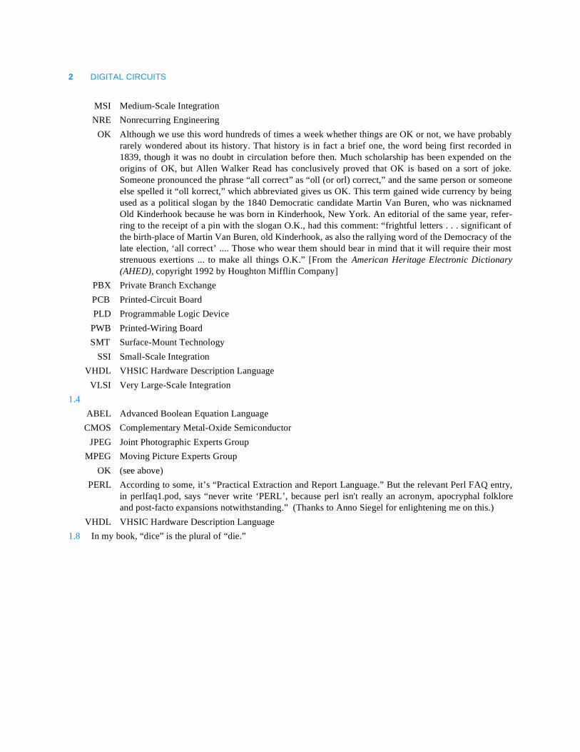
1.2 Three definitions of “bit”:(1) A binary digit (p. 1). (2) Past tense of “bite” (p. 1). (3) A small amount (pp. 6, 10).
1.3
ASIC Application-Specific Integrated Circuit
CAD Computer-Aided Design
CD Compact Disc
CO Central Office
CPLD Complex Programmable Logic Device
DAT Digital Audio Tape
DIP Dual In-line Pin
DVD Digital Versatile Disc
FPGA Field-Programmable Gate Array
HDL Hardware Description Language
IC Integrated Circuit
IP Internet Protocol
LSI Large-Scale Integration
MCM Multichip Module
2 DIGITAL CIRCUITS
MSI Medium-Scale Integration
NRE Nonrecurring Engineering
OK Although we use this word hundreds of times a week whether things are OK or not, we have probablyrarely wondered about its history. That history is in fact a brief one, the word being first recorded in1839, though it was no doubt in circulation before then. Much scholarship has been expended on theorigins of OK, but Allen Walker Read has conclusively proved that OK is based on a sort of joke.Someone pronounced the phrase “all correct” as “oll (or orl) correct,” and the same person or someoneelse spelled it “oll korrect,” which abbreviated gives us OK. This term gained wide currency by beingused as a political slogan by the 1840 Democratic candidate Martin Van Buren, who was nicknamedOld Kinderhook because he was born in Kinderhook, New York. An editorial of the same year, refer-ring to the receipt of a pin with the slogan O.K., had this comment: “frightful letters . . . significant ofthe birth-place of Martin Van Buren, old Kinderhook, as also the rallying word of the Democracy of thelate election, ‘all correct’ .... Those who wear them should bear in mind that it will require their moststrenuous exertions ... to make all things O.K.” [From the American Heritage Electronic Dictionary(AHED), copyright 1992 by Houghton Mifflin Company]
PBX Private Branch Exchange
PCB Printed-Circuit Board
PLD Programmable Logic Device
PWB Printed-Wiring Board
SMT Surface-Mount Technology
SSI Small-Scale Integration
VHDL VHSIC Hardware Description Language
VLSI Very Large-Scale Integration
1.4
ABEL Advanced Boolean Equation Language
CMOS Complementary Metal-Oxide Semiconductor
JPEG Joint Photographic Experts Group
MPEG Moving Picture Experts Group
OK (see above)
PERL According to some, it’s “Practical Extraction and Report Language.” But the relevant Perl FAQ entry,in perlfaq1.pod, says “never write ‘PERL’, because perl isn't really an acronym, apocryphal folkloreand post-facto expansions notwithstanding.” (Thanks to Anno Siegel for enlightening me on this.)
VHDL VHSIC Hardware Description Language
1.8 In my book, “dice” is the plural of “die.”
2–1
E X E R C I S E S O L U T I O N S
NUMBER SYSTEMS AND CODES
2
2.1 (a) (b)
(c) (d)
(e) (f)
(g) (h)
(i) (j)
2.3 (a)
(b)
(c)
(d)
(e)
(f)
2.5 (a) (b)
(c) (d)
(e) (f)
(g) (h)
(i) (j)
11010112 6B16= 1740038 11111000000000112=
101101112 B716= 67.248 110111.01012=
10100.11012 14.D16= F3A516 11110011101001012=
110110012 3318= AB3D16 10101011001111012=
101111.01112 57.348= 15C.3816 101011100.001112=
102316 10000001000112 100438= =
7E6A16 1111110011010102 771528= =
ABCD16 10101011110011012 1257158= =
C35016 11000011010100002 1415208= =
9E36.7A16 1001111000110110.01111012 117066.3648= =
DEAD.BEEF16 1101111010101101.10111110111011112 157255.5756748= =
11010112 10710= 1740038 6349110=
101101112 18310= 67.248 55.312510=
10100.11012 20.812510= F3A516 6237310=
120103 13810= AB3D16 4383710=
71568 369410= 15C.3816 348.2187510=
2–2 DIGITAL CIRCUITS
2.6 (a) (b)
(c) (d)
(e) (f)
(g) (h)
(i) (j)
2.7 (a) (b) (c) (d)
2.10 (a) (b) (c) (d)
2.11
2.18
Suppose a 3n-bit number B is represented by an n-digit octal number Q. Then the two’s-complement of B isrepresented by the 8’s-complement of Q.
2.22 Starting with the arrow pointing at any number, adding a positive number causes overflow if the arrow isadvanced through the +7 to –8 transition. Adding a negative number to any number causes overflow if thearrow is not advanced through the +7 to –8 transition.
12510 11111012= 348910 66418=
20910 110100012= 971410 227628=
13210 10001002= 2385110 5D2B16=
72710 104025= 5719010 DF6616=
143510 26338= 6511310 FE5916=
1100010
110101
+ 11001
1001110--------------------------
1011000
101110
+ 100101
1010011--------------------------
111111110
11011101
+ 1100011
101000000-----------------------------------
11000000
1110010
+ 1101101
11011111-----------------------------
1372
+ 4631
59A3--------------------
4F1A5
+ B8D5
5AA7A----------------------
F35B
+ 27E6
11B41---------------------
1B90F
+ C44E
27D5D----------------------
decimal + 18 + 115 +79 –49 –3 –100
signed-magnitude 00010010 01110011 01001111 10110001 10000011 11100100
two’s-magnitude 00010010 01110011 01001111 11001111 11111101 10011100
one’s-complement 00010010 01110011 01001111 11001110 11111100 10011011
hj b4j i+ 2j⋅
i 0=
3
∑=
Therefore,
B bi 2i⋅i 0–
4n 1–
∑ hi 16i⋅i 0=
n 1–
∑= =
B– 24n bii 0=
4n 1–
∑ 2i⋅– 16n hi 16i⋅i 0=
n 1–
∑–= =
EXERCISE SOLUTIONS 2–3
2.24 Let the binary representation of be . Then we can write the binary representation of as
, where . Note that is the sign bit of . The value of is
Case 1 In this case, if and only if , which is true if andonly if all of the discarded bits are 0, the same as .
Case 2 In this case, if and only if , whichis true if and only if all of the discarded bits are 1, the same as .
2.25 If the radix point is considered to be just to the right of the leftmost bit, then the largest number is andthe 2’s complement of is obtained by subtracting it from 2 (singular possessive). Regardless of the positionof the radix point, the 1s’ complement is obtained by subtracting from the largest number, which has all 1s(plural).
2.28
Case 1 First term is 0, summation terms have shifted coefficients as specified. Overflow if.
Case 2 Split first term into two halves; one half is cancelled by summation term if. Remaining half and remaining summation terms have shifted coefficients as specified. Overflow if.
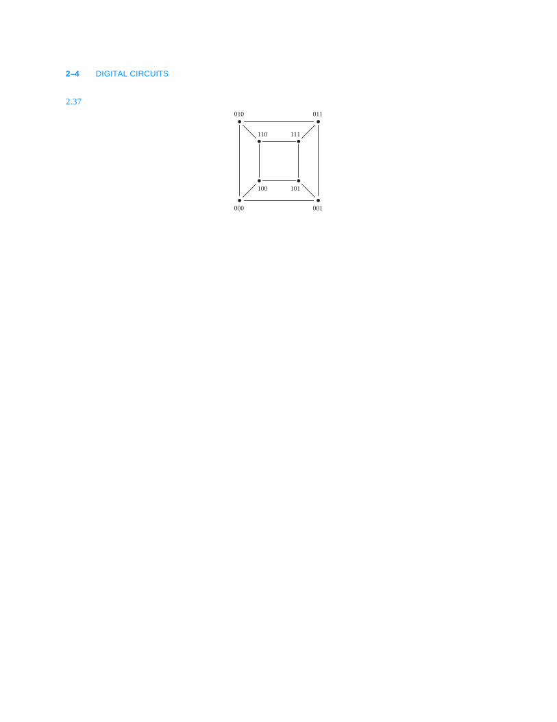
2.32 001–010, 011–100, 101–110, 111–000.
2.34 Perhaps the designers were worried about what would happen if the aircraft changed altitude in the middle of atransmission. With the Gray code, the codings of “adjacent” alitudes (at 50-foot increments) differ in only onebit. An altitude change during transmission affects only one bit, and whether the changed bit or the original istransmitted, the resulting code represents an altitude within one step (50 feet) of the original. With a binarycode, larger altitude errors could result, say if a plane changed from 12,800 feet (0001000000002) to 12,750feet (0000111111112) in the middle of a transmission, possibly yielding a result of 25,500 feet(0001111111112).
X xn 1– xn 2– …x1x0 Y
xmxm 1– …x1x0m n d–= xm 1– Y Y
Y 2m 1–– xm 1– xi 2i⋅i 0=
n 2–
∑+⋅=
The value of X is
X 2n 1–– xn 1– xi 2i⋅i 0=
n 2–
∑+⋅=
2n 1–– xn 1– Y 2m 1– xm 1–⋅ xi 2i⋅i m 1–=
n 2–
∑+ + +⋅=
2n 1–– xn 1– Y 2 2m 1–⋅ xi 2i⋅i m=
n 2–
∑+ + +⋅=
xm 1– 0=( ) X Y= 2n 1–– xn 1–⋅ xi 2i⋅i m=n 2–∑+ 0=
xm…xn 1–( ) xm 1–
xm 1– 1=( ) X Y= 2n 1–– xn 1–⋅ 2 2m 1–⋅ xi 2i⋅i m=n 2–∑+ + 0=
xm…xn 1–( ) xm 1–
1.11…1D
D
B bn 1–– 2n 1–⋅ bi 2i⋅i 0=
n 2–
∑+=
2B bn 1–– 2n bi 2i 1+⋅i 0=
n 2–
∑+⋅=
bn 1– 0=( )bn 2– 1=
bn 1– 1=( ) bn 2– 2n 1–⋅bn 2– 1=bn 2– 0=
2–4 DIGITAL CIRCUITS
2.37 010 011
000 001
111110
100 101
3–1
E X E R C I S E S O L U T I O N S
DIGITAL CIRCUITS
3
3.1 The “probably” cases may cause damage to the gate if sustained.
3.3 A logic buffer is a non-linear amplifier that maps the entire set of possible analog input voltages into just twooutput votages, HIGH and LOW. An audio amplifier has a linear response over its specified operating range,mapping each input voltage into an output voltage that is directly proprtional to the input voltage.
3.6 From the American Heritage Electronic Dictionary (AHED), copyright 1992 by Houghton Mifflin Company:
(1) A structure that can be swung, drawn, or lowered to block an entrance or a passageway.
(2) a. An opening in a wall or fence for entrance or exit. b. The structure surrounding such an opening, such asthe monumental or fortified entrance to a palace or walled city.
(3) a. A means of access: the gate to riches. b. A passageway, as in an airport terminal, through which passen-gers proceed for embarkation.
(4) A mountain pass.
(5) The total paid attendance or admission receipts at a public event: a good gate at the football game.
(6) A device for controlling the passage of water or gas through a dam or conduit.
(7) The channel through which molten metal flows into a shaped cavity of a mold.
(8) Sports. A passage between two upright poles through which a skier must go in a slalom race.
(9) Electronics. A circuit with multiple inputs and one output that is energized only when a designated set ofinput pulses is received.
(a) 0 (b) 1 (c) 0 (d) undefined
(e) 1 (f) probably 1 (g) probably 0 (h) probably 0
3–2 DIGITAL CIRCUITS
Well, definition (9) is closest to one of the answers that I had in mind. The other answer I was looking for is thegate of a MOS transistor.
3.14 A CMOS inverting gate has fewer transistors than a noninverting one, since an inversion comes “for free.”
3.15 Simple, inverting CMOS gates generally have two transistors per input. Four examples that meet the require-ments of the problem are 4-input NAND , 4-input NOR , 2-in, 2-wide AND–OR–INVERT , and 2-in, 2-wide OR–AND–INVERT.
3.18 One way is that a romance could be sparked, and the designers could end up with a lot less time to do theirwork. Another way is that the stray perfume in the IC production line could have contaminated the circuits usedby the designers, leading to marginal operation, more debugging time by the deidicated designers, and less timefor romance. By the way, the whole perfume story may be apocryphal.
3.20 Using the maximum output current ratings in both states, the HIGH-state margin is 0.69V and the LOW-statemargin is 1.02V. With CMOS loads (output currents less than 20 µA), the margins improve to 1.349V and1.25V, respectively.
3.21 The first answer for each parameter below assumes commercial operation and that the device is used with themaximum allowable (TTL) load. The number in parentheses, if any, indicates the value obtained under a lesserbut specified (CMOS) load.
VOHmin 3.84V (4.4V )
VIHmin 3.15V
VILmax 1.35V
VOLmax 0.33V (0.1V)
IImax 1µA
IOLmax 4 mA (20 µA)
IOHmax -4 mA (-20 µA)
3.22 Current is positive if it flows into a node. Therefore, an output with negative current is sourcing current.
3.23 The 74HC00 output drive is so weak, it’s not good for driving much:
(a) Assume that in the LOW state the output pulls down to 0.33V (the maximum spec). Then the output
current is , which is way more than the 4-mA commercial spec.
(b) For this problem, you first have to find the Thévenin equivalent of the load, or in series with
. In the HIGH state, the gate must pull the output up to 3.84V, a difference of 1.59V across ,
requiring 10.7 mA, which is out of spec. In the LOW state, we have a voltage drop of across
, so the output must sink 12.9 mA, again out of spec.
3.24 (In the first printing, change “74FCT257T” to “74HC00.”) The specification for the 74HC00 shows a maxi-mum power-supply current of 10 µA when the inputs aree at 0 or 5V, but based on the discussion inSection 3.5.3 we would expect the current to be more when the inputs are at their worst-case values (1.35 or3.15V). If we consider “nonlogic” input values, the maximum current will flow if the inputs are held right atthe switching threshold, approximately VCC/2.
3.26 (In the first printing, change “74FCT257T” to “74HC00.”) Using the formulas on page 119, we can estimatethat or, using the higher value of in the spec, that
. (The discrepancy shows that the output characteristic of this deviceis somewhat nonlinear.) We can also estimate .
3.29 The purpose of decoupling capacitors is to provide the instantaneous power-supply current that is required dur-ing output transitions. Printed-circuit board traces have inductance, which acts as a barrier to current flow athigh frequencies (fast transition rates). The farther the capacitor is from the device that needs decoupling, thelarger is the instantaneous voltage drop across the connecting signal path, resulting in larger spike (up or down)in the device’s power-supply voltage.
VOL
5.0V( ) 120Ω⁄ 41.7mA=
148.5Ω2.25V 148.5Ω
2.25V 0.33V–
148.5Ω
Rp(on) 5.0 3.84–( ) 0.004⁄ 290Ω= = VOHminRp(on) 5.0 4.4–( ) 0.00002⁄ 30KΩ= =
Rn(on) 0.33 0.004⁄ 82.5Ω= =
EXERCISE SOLUTIONS 3–3
3.32 (a) 5 ns.
3.38 Smaller resistors result in shorter rise times for LOW-to-HIGH transitions but higher power consumption in theLOW state. Stated another way, larger resistors result in lower power consumption in the LOW state but longerrise times (more ooze) for LOW -to-HIGH transitions.
3.39 The resistor must drop with 5mA of current through it. Therefore; a good standard value would be .
3.41 (The Secret of the Ooze.) The wired output has only passive pull-up to the HIGH state. Therefore, the time forLOW-to-HIGH transitions, an important component of total delay, depends on the amount of capacitive loadingand the size of the pull-up resistor. A moderate capacitive load (say, 100 pF) and even a very strong pull-upresistor (say, ) can still lead to time constants and transition times (15 ns in this example) that are longerthan the delay of an additional gate with active pull-up.
3.42 The winner is 74FCT-T—48 mA in the LOW state and 15 mA in the HIGH state (see Table 3–8). TTL familiesdon’t come close.
3.46 n diodes are required.
3.49 For each interfacing situation, we compute the fanout in the LOW state by dividing of the driving gateby of the driven gate. Similarly, the fanout in the HIGH state is computed by dividing of thedriving gate by of the driven gate. The overall fanout is the lower of these two results.
3.50 For the pull-down, we must have at most a 0.5-V drop in order to create a that is no worse than a standardLS-TTL output driving the input. Since , we get and
. (Alternatively, )
For the pull-up, we must have at most a 2.3-V drop in order to create a that is no worse than a standardLS-TTL output driving the input. Since , we get and
. (Alternatively, we could have calculated the result as.) The pull-up dissipates less power.
3.52 The main benefit of Schottky diodes is to prevent transistors from saturating, which allows them to switch morequickly. The main drawback is that they raise the collector-to-emitter drop across an almost-saturated transis-tor, which decreases LOW -state noise margin.
3.55
Low-state High-state Overall Excess
Case Ratio Fanout Ratio Fanout Fanout State Drive
74LS driving 74LS 20 20 20 none
74LS driving 74S 4 8 4 HIGH
LOW-state HIGH-state
OK? OK?
470 — 5.0 470 4.5 9.57 no <0 — yes
330 470 2.9375 193.875 2.4375 12.57 no <0 — yes
5.0 2.0– 0.37– 2.63V=r 2.63 0.005⁄ 526Ω= = 510Ω
150Ω
IOLmaxI ILmax IOLmax
I IHmax
8mA0.4mA---------------- 400µA
20µA-----------------
8mA2mA------------ 400µA
50µA----------------- 200µA
VILI ILmax 0.4mA= Rpd 0.5 0.004⁄ 1250Ω= =
Ppd VIL2 Rpd⁄ 0.5( )2 1250⁄ 0.2mW= = = Ppd VIL I IL 0.5 0.0004⋅ 0.2mW= = =
VIHI IHmax 20µA= Rpu 2.3 0.00002⁄ 115kΩ= =
Ppu VIH2 Rpu⁄ 2.3( )2 115000⁄ 0.046mW= = =
Ppu VIHI IH 2.3 0.00002⋅ 0.046mW= = =
RVCCΩ( )
RGNDΩ( )
VThevV( )
RThevΩ( )
VThev VOLV( )– IOL
mA( )VOH VThev
V( )– IOH
µA( )
3–4 DIGITAL CIRCUITS
3.56
3.57 For each interfacing situation, we compute the fanout in the LOW state by dividing of the driving gateby of the driven gate. Similarly, the fanout in the HIGH state is computed by dividing of thedriving gate by of the driven gate. The overall fanout is the lower of these two results.
3.64 TTL-compatible inputs have , and typical TTL outputs have . CMOS outputlevels are already high compared to these levels, so there’s no point in wasting silicon to make them any higherby lowering the voltage drop in the HIGH state.
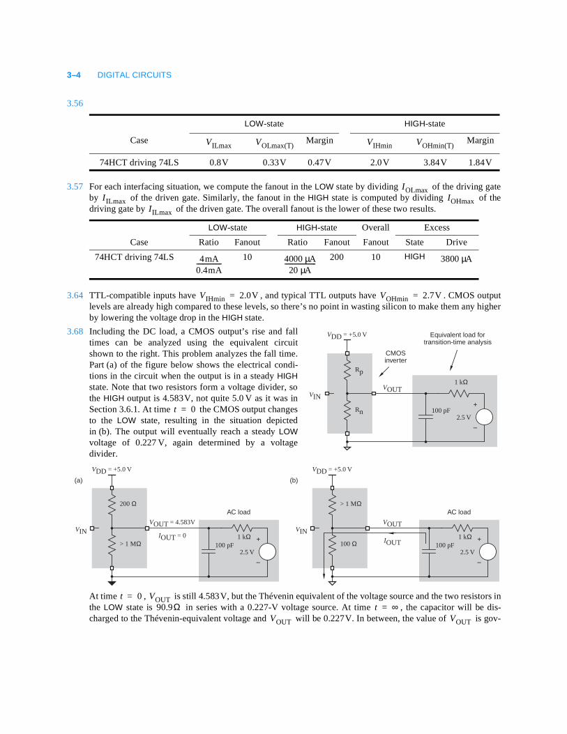
3.68 Including the DC load, a CMOS output’s rise and falltimes can be analyzed using the equivalent circuitshown to the right. This problem analyzes the fall time.Part (a) of the figure below shows the electrical condi-tions in the circuit when the output is in a steady HIGHstate. Note that two resistors form a voltage divider, sothe HIGH output is 4.583V, not quite 5.0 V as it was inSection 3.6.1. At time the CMOS output changesto the LOW state, resulting in the situation depictedin (b). The output will eventually reach a steady LOWvoltage of 0.227 V, again determined by a voltagedivider.
At time , is still 4.583V, but the Thévenin equivalent of the voltage source and the two resistors inthe LOW state is in series with a 0.227-V voltage source. At time , the capacitor will be dis-charged to the Thévenin-equivalent voltage and will be 0.227V. In between, the value of is gov-
LOW-state HIGH-state
Case Margin Margin
74HCT driving 74LS 0.8V 0.33V 0.47V 2.0V 3.84V 1.84V
LOW-state HIGH-state Overall Excess
Case Ratio Fanout Ratio Fanout Fanout State Drive
74HCT driving 74LS 10 200 10 HIGH
VILmax VOLmax(T) VIHmin VOHmin(T)
IOLmaxI ILmax IOHmax
I ILmax
4mA0.4mA---------------- 4000µA
20 µA-------------------- 3800µA
VIHmin 2.0V= VOHmin 2.7V=
VDD = +5.0 V
VOUTVIN
Rn
Rp
CMOSinverter
Equivalent load fortransition-time analysis
+
–
2.5 V
1 kΩ
100 pFt 0=
AC load
+
–
2.5 V
1 kΩ100 pF
VDD = +5.0 V
VOUT = 4.583V
IOUT = 0IOUT
VIN
> 1 MΩ
200 ΩAC load
VDD = +5.0 V
VOUTVIN
(a) (b)
100 Ω
> 1 MΩ
+
–
2.5 V
1 kΩ100 pF
t 0= VOUT90.9Ω t ∞=
VOUT VOUT
EXERCISE SOLUTIONS 3–5
erned by an exponential law:
Because of the DC load resistance, the time constant is a little shorter than it was in Section 3.6.1, at 9.09 ns.
To obtain the fall time, we must solve the preceding equation for VOUT = 3.5 and VOUT = 1.5, yielding
The fall time is the difference between these two numbers, or 7.7 ns. This is slightly shorter than the 8.5 nsresult in Section 3.6.1 because of the slightly shorter time constant.
3.70 The time constant is . We solve the rise-time equation for the point at which VOUT is1.5 V, as on p. 118 of the text:
3.77 The LSB toggles at a rate of 16 MHz. It takes two clock ticks for the LSB to complete one cycle, so the transi-tion frequency is 8 MHz. The MSB’s frequency is 27 times slower, or 62.5 KHz. The LSB’s dynamic power isthe most significant, but the sum of the transitions on the higher order bits, a binary series, is equivalent toalmost another 8 MHz worth of transitions on a single output bit. Including the LSB, we have almost 16 MHz,but applied to the load capacitance on just a single output. If the different ouputs actually have different loadcapacitances, then a weighted average would have to be used.
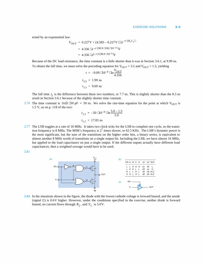
3.81
3.84 In the situations shown in the figure, the diode with the lowest cathode voltage is forward biased, and the anode(signal C) is 0.6V higher. However, under the conditions specified in the exercise, neither diode is forwardbiased, no current flows through , and is 5.0V.
VOUT 0.227V 4.583 0.227V–( )+ e t RnCL( )⁄–⋅=
4.356 e t 90.9 100 1012–⋅ ⋅( )⁄– V⋅=
4.356 e t–( ) 90.9 10 9–⋅( )⁄ V⋅=
t 9.09– 10 9–VOUT
4.356-------------ln⋅⋅=
t3.5 1.99 ns=
t1.5 9.69 ns=
tf
1kΩ 50 pF⋅ 50 ns=
t1.5 50– 10 9– 5.0 1.5–5.0
---------------------ln⋅⋅=
t1.5 17.83 ns=
VCC
A
EN
OUT
Q1
Q2
EN
LLHH
A
LHLH
B
HHLL
C
HLHH
D
HLLL
Q1
onoffoffoff
Q2
offonoffoff
OUT
LH
Hi-ZHi-Z
EN
A OUT
(a) (b)
(c)
BC
D
R2 VC
3–6 DIGITAL CIRCUITS
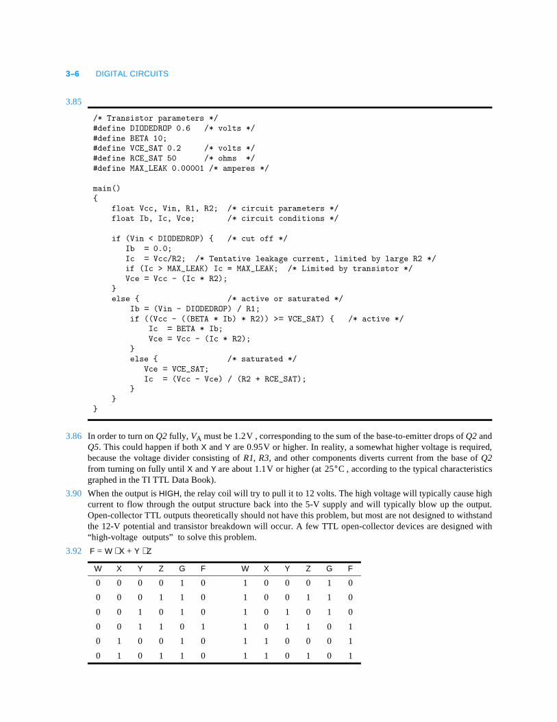
3.85
3.86 In order to turn on Q2 fully, VA must be 1.2V , corresponding to the sum of the base-to-emitter drops of Q2 andQ5. This could happen if both X and Y are 0.95V or higher. In reality, a somewhat higher voltage is required,because the voltage divider consisting of R1, R3, and other components diverts current from the base of Q2from turning on fully until X and Y are about 1.1V or higher (at , according to the typical characteristicsgraphed in the TI TTL Data Book).
3.90 When the output is HIGH, the relay coil will try to pull it to 12 volts. The high voltage will typically cause highcurrent to flow through the output structure back into the 5-V supply and will typically blow up the output.Open-collector TTL outputs theoretically should not have this problem, but most are not designed to withstandthe 12-V potential and transistor breakdown will occur. A few TTL open-collector devices are designed with“high-voltage outputs” to solve this problem.
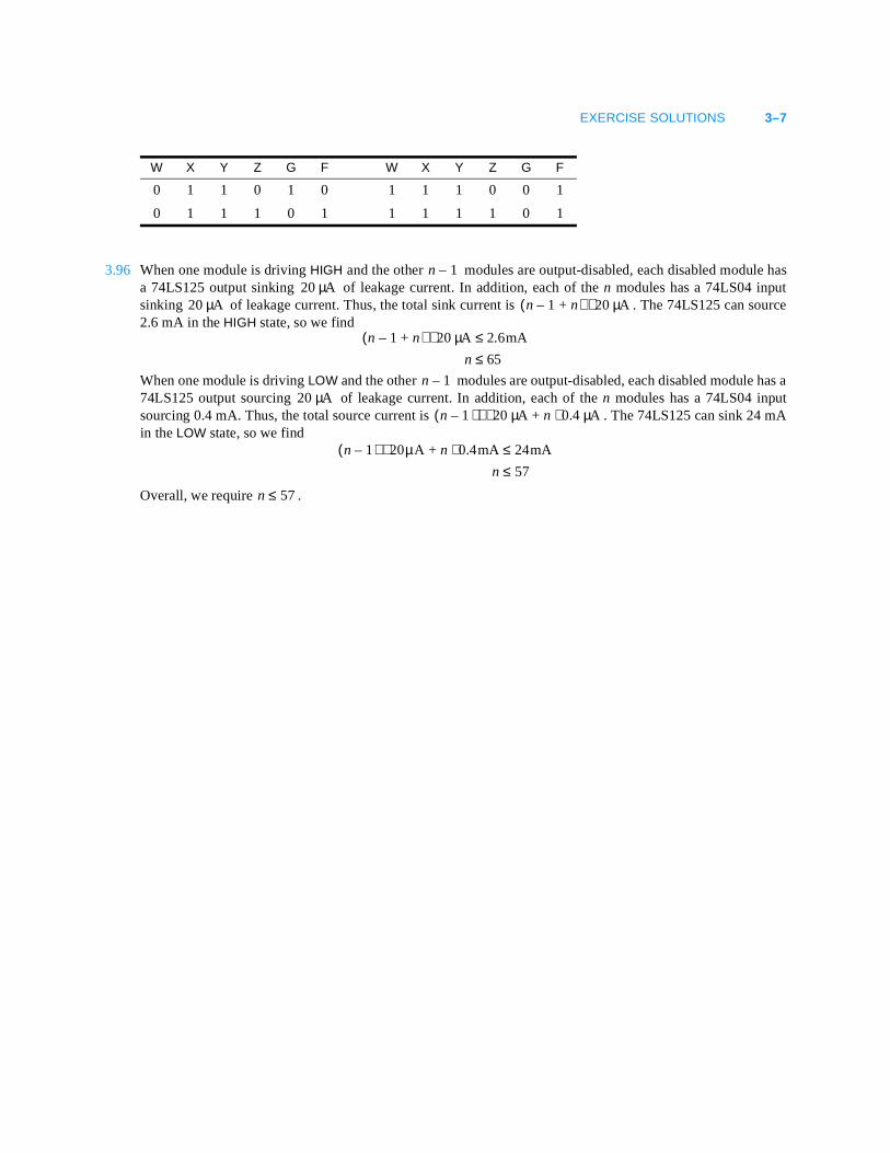
3.92 F = W ⋅ X + Y ⋅ Z
/* Transistor parameters */#define DIODEDROP 0.6 /* volts */#define BETA 10;#define VCE_SAT 0.2 /* volts */#define RCE_SAT 50 /* ohms */#define MAX_LEAK 0.00001 /* amperes */
main() float Vcc, Vin, R1, R2; /* circuit parameters */ float Ib, Ic, Vce; /* circuit conditions */
if (Vin < DIODEDROP) /* cut off */ Ib = 0.0; Ic = Vcc/R2; /* Tentative leakage current, limited by large R2 */ if (Ic > MAX_LEAK) Ic = MAX_LEAK; /* Limited by transistor */ Vce = Vcc - (Ic * R2); else /* active or saturated */ Ib = (Vin - DIODEDROP) / R1; if ((Vcc - ((BETA * Ib) * R2)) >= VCE_SAT) /* active */ Ic = BETA * Ib; Vce = Vcc - (Ic * R2); else /* saturated */ Vce = VCE_SAT; Ic = (Vcc - Vce) / (R2 + RCE_SAT);
W X Y Z G F W X Y Z G F
0 0 0 0 1 0 1 0 0 0 1 0
0 0 0 1 1 0 1 0 0 1 1 0
0 0 1 0 1 0 1 0 1 0 1 0
0 0 1 1 0 1 1 0 1 1 0 1
0 1 0 0 1 0 1 1 0 0 0 1
0 1 0 1 1 0 1 1 0 1 0 1
25°C
EXERCISE SOLUTIONS 3–7
3.96 When one module is driving HIGH and the other modules are output-disabled, each disabled module hasa 74LS125 output sinking of leakage current. In addition, each of the n modules has a 74LS04 inputsinking of leakage current. Thus, the total sink current is . The 74LS125 can source2.6 mA in the HIGH state, so we find
When one module is driving LOW and the other modules are output-disabled, each disabled module has a74LS125 output sourcing of leakage current. In addition, each of the n modules has a 74LS04 inputsourcing 0.4 mA. Thus, the total source current is . The 74LS125 can sink 24 mAin the LOW state, so we find
Overall, we require .
0 1 1 0 1 0 1 1 1 0 0 1
0 1 1 1 0 1 1 1 1 1 0 1
W X Y Z G F W X Y Z G F
n 1–20µA
20µA n 1– n+( ) 20µA⋅
n 1– n+( ) 20µA⋅ 2.6mA≤n 65≤
n 1–20 µA
n 1 )–( ) 20 µA⋅ n 0.4µA⋅+
n 1–( ) 20µA⋅ n 0.4mA⋅+ 24mA≤n 57≤
n 57≤
4–1
E X E R C I S E S O L U T I O N S
COMBINATIONALLOGIC DESIGN PRINCIPLES
4
4.2
4.3
4.4
T2:= 1
0 1 = 1
1 1 = 1
X X 1+
T3:=
0 0 = 0
1 1 = 1
X X X+ X
=
0 0 = 0
1 1 = 1
T3′X X X⋅ X
=
0 0 0 = 0
0 1 1 = 1
1 0 1 = 1
1 1 1 = 1
T6
X Y X Y+ Y X+
4–2 DIGITAL CIRCUITS
4.5 The original expression assumes precedence of over , that is, the expression is . The paren-thesization must be retained for the correct result, , or the precedence must be swapped.
4.6 The answers for parts (a), (b), (c) are as follows.
4.7 (a) (b)
4.9
(a)
(b)
4.12 (1) Including inverters makes the problem too difficult. (2) In modern PLD-based designs, inverters do costnothing and really can be ignored.
4.13
⋅ + X Y Z⋅( )+X ′ Y′ Z′+( )⋅
W X Y Z (W X Y Z′ W+ X ′ Y Z W′+ X Y Z W+ X Y′ Z)⋅ ⋅ ⋅ ⋅ ⋅ ⋅ ⋅ ⋅ ⋅ ⋅ ⋅ ⋅ ⋅ ⋅ ⋅ ⋅W X Y Z W X Y Z′ W X Y Z W X′ Y⋅ ⋅ ⋅ ⋅ ⋅ ⋅+ Z W X Y Z W′ X Y Z⋅ ⋅ ⋅ ⋅ ⋅ ⋅ ⋅ W X Y Z W X Y′ Z (T8)⋅ ⋅ ⋅ ⋅ ⋅ ⋅ ⋅+ +⋅ ⋅ ⋅ ⋅ ⋅ ⋅ ⋅ ⋅=
0 0 0 0 T6′ T5′ T2′, ,( )+ + +=
0 A4′( )=
X Y Z F
0 0 0 0
0 0 1 1
0 1 0 1
0 1 1 1
1 0 0 0
1 0 1 0
1 1 0 0
1 1 1 0
W X Y Z F
0 0 0 0 1
0 0 0 1 1
0 0 1 0 0
0 0 1 1 1
0 1 0 0 1
0 1 0 1 1
0 1 1 0 1
0 1 1 1 1
1 0 0 0 1
1 0 0 1 1
1 0 1 0 0
1 0 1 1 1
1 1 0 0 1
1 1 0 1 0
1 1 1 0 0
1 1 1 1 0
F X ′ Y Y′ X⋅+⋅ X( Y ) X′ Y′+( )⋅+= =
F A B⋅ A B+( ) A B ′+( ) A′ B+( )⋅⋅= =
1
1 11 1
X ⋅ Y
Z
00 01 11 10
X Y
0
X
Y
Z1
Z
F = X ⋅ Y + Z
(a)
F = W′ ⋅ X + X′ ⋅ Y′ ⋅ Z + X ⋅ Y
00 01 11 10
W X
Y Z
00
1 1
1
1
1
1
11
11
10
W
X
Y
Z
X ⋅ Y
X′ ⋅ Y′ ⋅ Z′
W′ ⋅ X
(b)
01
W′ ⋅ Y′ ⋅ Z
EXERCISE SOLUTIONS 4–3
4.14
4.15 (a) Cost is less —one less gate input.
4.19
4.20
4.21 For the minimal sum-of-products expression to equal the minimal product-of-sums expression, the correspond-ing maps must have the opposite don’t-cares covered, so that the expressions yield the same value for the don’t-care input combinations.
(a) Both mininal sum-of-products expressions cover cell 15; they are equal. The minimal product-of-sumsexpression also covers cell 15, so the expressions are not equal. The s-of-p and p-of-s expressions require thesame number of gates, but the p-of-s requires one fewer input.
(b) Both mininal sum-of-products expressions cover cell 3 and 9 and not 15; they are equal. The minimalproduct-of-sums expression covers cell 15, and not 3 or 9, so the expressions are equal. The p-of-s expressionrequires fewer gates and inputs.
11 1
Y′ ⋅ Z′00 01 11 10
X Y
0
X
Y
Z1
Z
F′ = X′ ⋅ Z′ + X ⋅ Y′ + W ⋅ X ⋅ Y′
(b)(a)01 11
W X
Y Z
1 1
1
1
1
1 1
111
W
Y
Z01
X′ ⋅ Z′
X′ ⋅ Y
X′ ⋅ Z′W ⋅ X ⋅ Y′
X
F′ = X′ ⋅ Z′ + Y′ ⋅ Z′
00
00
10
10
W ⋅ Y′ ⋅ Z′
F = (X + Z) ⋅ (Y + Z)
F = (X + Z) ⋅ (X′ + Y) ⋅ (W′ + X′ + Y)
X′ + Z
X + Y′ + Z′ Y + Z
X′ + Z
X + Y′ + Z′
Y + Z
0
00 01 11 10X Y
Z
X
Y
Z0
0 0
1
0
X
Y′
Z′
X′
Z
Y
F
F = W′ ⋅ Y′ ⋅ Z + W′ ⋅ X′ ⋅ Z + W ⋅ X ⋅ Y
+ W′ ⋅ X′ ⋅ Y′ or X′ ⋅ Y′ ⋅ Z′
00 01 11 10
W X
Y Z
1 1
1
1
d
d
1
11
10
W
X
Y
Z
W ⋅ X ⋅ Y
X′ ⋅ Y′ ⋅ Z′(a)
01
W′ ⋅ X′ ⋅ Y′
W′ ⋅ X′ ⋅ Z
W′ ⋅ Y′ ⋅ Z
00
F = W′ ⋅ X′ + X′ ⋅ Y′ + X′ ⋅ Z
00 01 11 10
W X
Y Z
1
1
1
d
d d 1
1
10
W
X
Y
Z
W ⋅ Y ⋅ Z
X′ ⋅ Y′(b)
W′ ⋅ X′
00
11
X′ ⋅ Z
01
F = (W + X′ + Y′) ⋅ (X′ + Y + Z) ⋅ (W′ + Z′) ⋅ (X + Y′ + Z)
00 11 10
W X
Y Z
0 0
0 0
0 0
d
d
000
W
X
Y
Z
W′ + Z
X + Y′ + Z
W′ + Y
W′ + X
(a)
01
X′ + Y′ + Z′W + X′ + Z
W + Y′ + Z
W + X′ + Y′
00
F = X′ ⋅ (W′ + Y′ + Z)
00 01 11 10
W X
Y Z
0 0
0
0 0 0
d
d d0
0
10
W
X
Y
Z
W′ + Y′ + Z
W′ + Y + Z′
X′(b)
01
00
11
10
11
01
W + Y′ + Z′
X′ + Y + Z
4–4 DIGITAL CIRCUITS
4.22 Consensus terms that must be added to cover the hazards are “circled” with rectangles.
4.28
4.29
4.31
4.35
4.37 Figure 3–4(d) is more appropriate, since electrically a TTL NOR gate is just the wired-AND of inverters.
4.39
(a) True. If then either or . If then either or . Therefore,
, and .
Analyzing this circuit with the standardmethod for feedback sequential circuits(Section 5.5), we get the followingexcitation equation:
Thus, is a function of X alone, andis independent of the circuit’s previous“state.”
11
1
1
00 01 11 10
W X
0
W
X
Y1
Y
W′ ⋅ Y′
00
W X
Y Z
11
1
1
1
1
1
W
X
Y
Z
W ⋅ X′ ⋅ Y′
W ⋅ Y′ ⋅ Z
(b)(a)
01
00
11
01
X ⋅ Z10
X ⋅ Y′
W ⋅ X
X ⋅ Y
11 10
1
X ⋅ Y′ ⋅ Z
X
QY
Q∗ X′ Y Q⋅( )′ Q+( )⋅=
X′ Y ′ Q ′ Q+ +( )⋅=
X′ 1⋅= X ′=
Q∗
X 1⋅ X (T1′)=
X Y Y′+( )⋅ X (T5)=
X Y⋅ X Y′⋅+ X (T8)=
X Y ′+( ) Y⋅ X Y⋅ Y ′ Y (T8)⋅+=
X Y⋅ Y Y′ (T6′)⋅+=
X Y⋅ 0 (T5′)+=
X Y (T1)⋅=
X1 X2 … Xn Xn⋅ ⋅ ⋅ ⋅ X1 X2 … Xn Xn⋅( ) (T6′, T7′ as required)⋅ ⋅ ⋅=
X1 X2 … Xn (T3′)⋅ ⋅ ⋅=
X1 X2 … Xn Xn+ + + + X1 X2 … Xn Xn+( ) (T6, T7 as required)+ + +=
X1 X2 … Xn+ + +( ) (T3)=
A B⋅ 0= A 0= B 0= A B+ 1= A 1= B 1=
A B, 0 1 or 1,0,= A B ′=
EXERCISE SOLUTIONS 4–5
4.41
A dual theorem may be written based on maxterms.
4.46 Yes, 2-input NAND gates form a completeset of logic gates. We prove the result inthe figure on the right by showing thatthese gates can be used to make 2-inputAND gates, 2-input OR gates, and inverters,which form a complete set.
4.52 Take the dual, “multiply out,” and take thedual again. The result is the same as “add-ing out.”
4.58 (a) 16 ns. (c) 18 ns. (d) 10 ns.
4.61 To make it easier to follow, we’ll take thedual, multiply out, and then take the dualagain. Also, we’ll simplify using theorems and , otherwise we’ll get a nonminimal result for sure. ForFigure 4–27:
For Figure 4-29:
4.63
F X1 … Xi, X i 1+ … Xn, ,,,( ) X1′ … Xi ′, , F 0 … 0 Xi 1+ … Xn, , , , ,( )⋅=
X1′ … X i ′, , F 0 … 1 Xi 1+ … Xn, , , , ,( )⋅+
… X1′ … Xi ′, , F 1 … 1, , X i 1+ … Xn, , ,( )⋅+
2i minterms 2i combs
T3′ T6′
F X Z⋅ Y ′ Z⋅ X′ Y Z′⋅ ⋅+ +=
FD X Z+( ) Y′ Z+( ) X′ Y Z′+ +( )⋅⋅=
X Y ′ Z ′ X Z Y Z Y ′ X′ Z Y ′ X ′ Z Z X ′ Z Z Y(T8, T5′, T2′)⋅ ⋅+⋅ ⋅+⋅ ⋅+⋅ ⋅+⋅ ⋅+⋅ ⋅=
X Y ′ Z ′⋅ ⋅ X Y Z⋅ ⋅ X′ Y′ Z ′⋅ ⋅ X ′ Z⋅ Y Z (T3′, T6′)⋅+ + + +=
F X Y ′ Z ′+ +( ) X Y Z+ +( ) X ′ Y ′ Z+ +( ) X ′ Z+( ) Y Z+( ) (not minimal)⋅ ⋅ ⋅ ⋅=
F X Z ′⋅ Y′+=
FD X Z ′+( ) Y′⋅=
X Y ′ Z′ Y ′⋅ (T8)+⋅=
X Y ′⋅ Y ′ Z ′⋅ (T6′)+=
F X Y ′+( ) Y′ Z′+( ) (minimal)⋅=
1
1
00 01 11 10
W X
Y Z
00
1
1
1
1
01
11
10
W
X
Y
Z
XW′ ⋅ Y ⋅ Z′
W ⋅ Y′ ⋅ Z
W ⋅ X ⋅ Z
F = W′ ⋅ X ⋅ Y + W′ ⋅ Y ⋅ Z′ + W ⋅ Y′ ⋅ Z + W ⋅ X ⋅ Z
W′ ⋅ X ⋅ Y
4–6 DIGITAL CIRCUITS
4.69 For part (d), note that it is easiest to work with the product-of-sums directly; rather than multiplying out, onesimply enters the 0s on the map.
4.70 Note that in these maps are drawn for the “true” function and we’ve written sum terms for the prime implicates(the dual of prime implicants) directly, instead of using the complement method suggested in Section 4.3.6.
4.72
1
1 11 1
X
Z
00 01 11 10
X Y
0
X
Y
Z1
Z
F = X ⋅ Y + Z
(b)(a)
F = D
00 01 11 10
A B
C D
00
1
1
1
1
11
1 111
10
A
C
D
B
D
01
1 1 1 1
1
Y + Z00 01 11 10X Y
0
X
Y
Z1
Z
(b)(a)
00 01 11 10
A B
C D
00
1 1 11
1 1 1111
10
A
C
D01
D
X + Z
F = D
B
1
1
(a) V ⋅ W′ ⋅ Y′ ⋅ Z′
1 1
V = 0
01 11
1
11
W
X
Y
Z
X
01
V′ ⋅ X ⋅ Z
W X
Y Z
00
10
00
1
10
11
V = 1
01 11
1
11
W
X
Y
Z
X
01
W ⋅ X ⋅ Z
W X
Y Z
00
10
00
V ⋅ W ⋅ Z
1
1 1
10
V′ ⋅ X′ ⋅ Y′ ⋅ Z′
F = V′ ⋅ X ⋅ Z + V ⋅ W ⋅ Z + V ⋅ W′ ⋅ Y′ ⋅ Z′
(b) W′ ⋅ X′ ⋅ Y′ ⋅ Z′
1 1
V = 0
01 11
1
11
W
X
Y
Z
X
01
W X
Y Z
00
10
00
V′ ⋅ W ⋅ Y′
X ⋅ Y ⋅ Z V ⋅ X ⋅ Y
1
1
11
10
1
1
V = 1
01 11
11
W
X
Y
Z
X
01
W X
Y Z
00
10
00
1
1
10
F = V′ ⋅ W ⋅ Y′ + X ⋅ Y ⋅ Z + W′ ⋅ X′ ⋅ Y′ ⋅ Z′ + V ⋅ X ⋅ Y
EXERCISE SOLUTIONS 4–7
4.73 Note that in these maps are drawn for the “true” function and we’ve written sum terms for the prime implicates(the dual of prime implicants) directly, instead of using the complement method suggested in Section 4.3.6.
4.74
4.83 The name of the circuit comes from its output equation, F = 2B OR NOT 2B.
0
(a)
0 00
V = 0
01 11
0
00
0
W
X
Y
Z
0
01
W X
Y Z
00
00
0
10
V = 1
F = (V + Z) ⋅ (V + X) ⋅ (W′ + Z) ⋅ (V′ + W + Z′) ⋅ (Y′ + Z)
11
10
0
11
W
X
Y
Z01
W X
Y Z
00
00
0
0 0
00
00
0
0
0
0
10
11
10
01
0
(b)
V = 0
0
0
0
Y
X
0
0
0 0
0
0
0 0
V = 1
01
11Y
Z01
W X
Y Z
00
10
00
0
F = (X + Y′) ⋅ (V + Y′ + Z) ⋅ (V′ + W′ + Y′) ⋅ (W + X′ + Y′) ⋅ (W + Y + Z′) or (W + X + Z′)
01 11
WW X
00 10
Z11
01
00
10
Y Z
X XX
11
W
10
0
0 0 0
0
0
0
W′ + Z
V′ + W + Z′
Y′ + ZV + W + Y′
V + Y′ + Z
W + X + Z′
W + Y + Z′
W + X + Y′
W + X + Z′
V + Z
V + X
V′ + W′ + X
V′ + Y + Z
V′ + W′ + YV′ + X′ + Y
V′ + X + Z′
X + Y′
W + X′ + YV + W + X′ + Z
(a)
U,V = 0,0
1111
Y
X F = U′ ⋅ V′ ⋅ Y′ ⋅ Z + U′ ⋅ V ⋅ X ⋅ Z + X ⋅ Y′ ⋅ Z
U′ ⋅ V′ ⋅ Y′ ⋅ Z
01 11
WW X
00 10
Z11
01
00
10
Y Z
X
U,V = 0,1
1
11
1Y
XU′ ⋅ V ⋅ X ⋅ Z
01 11
WW X
00 10
Z11
01
00
10
Y Z
X
U,V = 1,0
11
Y
XX ⋅ Y′ ⋅ Z
01 11
WW X
00 10
Z11
01
00
10
Y Z
X
U,V = 1,1
11
Y
X
01 11
WW X
00 10
Z11
01
00
10
Y Z
X
3 t INV
2B
F
tOR
5–1
E X E R C I S E S O L U T I O N S
COMBINATIONALLOGIC DESIGN PRINCIPLES
574LS138
G2A
G1
G2B
Y0
Y1
Y2
Y3
6
4
5
15
14
13
7
B
A
C
Y4
Y5
Y6
Y7
1
12
11
10
92
3
5.4 READY′ is an expression, with ′ being a unary operator. Use a name like READY_L or /READY instead.
5.8 Both LOW-to-HIGH and HIGH-to-LOW transitions cause positive transitions on the outputs of three gates (everysecond gate), and negative transitions on the other three. Thus, the total delay in either case is
Since and for a 74LS00 are identical, the same result is obtained using a single worst-case delay of15 ns.
5.12 The smallest typical delay through one ’LS86 for any set of conditions is 10 ns. Use the rule of thumb, “mini-mum equals one-fourth to one-third of typical,” we estimate 3 ns as the minimum delay through one gate.Therefore, the minimum delay through the four gates is estimated at 12 ns.
The above estimate is conservative, as it does not take into account the actual transitions in the conditionsshown. For a LOW-to-HIGH input transition, the four gates have typical delays of 13, 10, 10, and 20 ns, a totalof 53 ns, so the minimum is estimated at one-fourth of this or 13 ns. For a HIGH-to-LOW input transition, thefour gates have typical delays of 20, 12, 12, and 13 ns, a total of 57 ns, so the minimum is estimated at 14 ns.
5.15 A decoder with active-low outputs ought to be faster, considering that this decoder structure can be imple-mented directly with inverting gates (which are faster than noninverting) as shown in Figures 5–35 and 5–37.
5.16 The worst-case ’138 output will have a transition in the same direction as the worst-case ’139 output, so we usetpHL numbers for both, which is the worst combination. The delay through the ’139 is 38 ns, and from the
tp 3tpLH(LS00) 3tpHL(LS00)+=
3 15⋅ 3 15⋅+=
90 ns=
tpLH tpHL
5–2 DIGITAL CIRCUITS
active-low enable input of the ’138 is 32 ns, for a total delay of 70 ns. Using “worst-case” numbers for the partsand ignoring the structure of the circuit, an overly pessimistic result of 79 ns is obtained.
We can also work the problem with 74HCT parts. Worst-case delay through the ’139 is 43 ns, and from theactive-low enable input of the ’138 is 42 ns, for a total delay of 85 ns. Ignoring the structure of the circuit, anoverly pessimistic result of 88 ns is obtained.
We can also work the problem with 74FCT parts. Worst-case delay through the ’139 is 9 ns, and from theactive-low enable input of the ’138 is 8 ns, for a total delay of 17 ns. Ignoring the structure of the circuit, aslightly pessimistic result of 18 ns is obtained.
Finally, we can work the problem with 74AHCT parts. Worst-case delay through the ’139 is 10.5 ns, and fromthe active-low enable input of the ’138 is 12 ns, for a total delay of 22.5 ns. Ignoring the structure of the circuit,a slightly pessimistic result of 23.5 ns is obtained.
5.19
5.21 Both halves of the ’139 are enabled simultaneously when EN_L is asserted. Therefore, two three-state driverswill be enabled to drive SDATA at the same time. Perhaps the designer forgot to put an extra inverter on thesignal going to 1G or 2G, which would ensure that exactly one source drives SDATA at all times.
5.22 The total delay is the sum of the decoding delay through the 74LS139, enabling delay of a 74LS151, and delaythrough a 74LS20: .
5.25 The worst-case delay is the sum of the delays through an ’LS280, select-to-output through an ’LS138, andthrough an ’LS86: .
5.30 The worst-case delay is the sum of four numbers:
• In U1, the worst-case delay from any input to C4 (22 ns).
• In U2, the worst-case delay from C0 to C4 (22 ns).
• In U3, the worst-case delay from C0 to C4 (22 ns).
• In U4, the worst-case delay from C0 to any sum output (24 ns).
Thus, the total worst-case delay is 90 ns.
5.35 With the stated input combination, Y5_L is LOW and the other outputs are HIGH . We have the following cases:
(a) Negating G2A_L or G2B_L causes Y5_L to go HIGH within 18 ns.
(b) Negating G1 causes Y5_L to go HIGH within 26 ns.
(c) Changing A or C causes Y5_L to go HIGH within 27 ns (the change propagates through 3 levels of logicinternally), and causes Y4_L or Y1_L respectively to go LOW within 41 ns (2 levels).
(d) Changing B causes Y5_L to go HIGH within 20 ns (2 levels), and causes Y7_L to go LOW within 39 ns (3
levels). The delays in the ’LS138 are very strange—the worst-case for 3 levels is shorter than for 2 levels!
5
74LS138
G2A
G1
G2B
Y0
Y1
Y2
Y3
15
14
13
7
B
A
C
Y4
Y5
Y6
Y7
12
11
10
9
74LS10
U2
1
2
13
12 F
6
4
1
2
3
Z
Y
X
+5 VR
5
74LS138
G2A
G1
G2B
Y0
Y1
Y2
Y3
15
14
13
7
B
A
C
Y4
Y5
Y6
Y7
12
11
10
9
74LS10
U2
12
1312 F
6
4
1
2
3
C
B
A
+5 VR
(a) (b)
U1U1
38 30 15+ + 83 ns=
50 41 30+ + 121 ns=
tpHL
EXERCISE SOLUTIONS 5–3
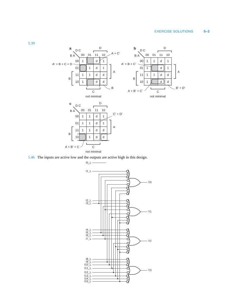
5.39
5.46 The inputs are active low and the outputs are active high in this design.
C
d
d
d
d d
d
11
1 1
1
1
1
B
01 11
DD C
00 10
A11
01
00
10
B A
D C
B A
D C
B A
A′ + B + C + D
A + B′ + C
A + C′
B
a
not minimal
C
d
d
d
d d
d
11
1 1
1
1
1 1
B
01 11
D
00 10
A11
01
00
10
A′ + B + C′
B′ + D′A + B′ + C′
b
not minimal
C
d
d
d
d d
d
11
1 1
1
1
1
1 1
B
01 11
D
00 10
A11
01
00
10
C′ + D′
c
not minimal
Y3
Y2
Y1
Y0
I1_L
I0_L
I2_LI3_L
I4_LI5_LI6_LI7_L
I8_LI9_L
I10_LI11_L
I12_LI13_LI14_LI15_L
5–4 DIGITAL CIRCUITS
5.47
I7
I6
I5I4
I3
I2
I1
I0
A2
I7_L
I6_L
I5_L
I4_L
I3_L
I2_L
I1_L
I0_L
A1
A0
GS
EO
EI
A2
A1
A0
IDLE
74x148
U1
9
U3
8
74x04
4
5
3
2
1
13
12
11
10
6
7
9
14
15
5
U3
6
11
U3
10
13
U3
12
I7
I6
I5
I4
I3
I2
I1
I0
11
U2
10
13
U2
12
1
U3
2
3
U3
4
3
U2
4
74x04
1
U2
2
5
U2
6
9
U2
8
EXERCISE SOLUTIONS 5–5
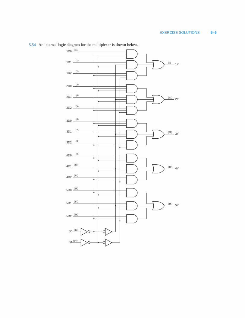
5.54 An internal logic diagram for the multiplexer is shown below.
1D2
1D1
1D0(23)
(1)
(2)
1Y(2)
2D2
2D1
2D0(3)
(4)
(5)
2Y(21)
3D2
3D1
3D0(6)
(7)
(8)
3Y(20)
4D2
4D1
4D0(9)
(10)
(11)
4Y(19)
S0
5D2
5D1
5D0
S1(14)
(13)
(18)
(17)
(16)
5Y(15)
5–6 DIGITAL CIRCUITS
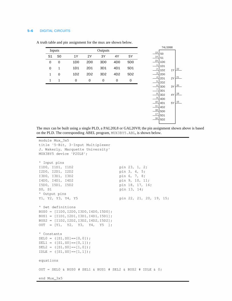
A truth table and pin assignment for the mux are shown below.
The mux can be built using a single PLD, a PAL20L8 or GAL20V8; the pin assignment shown above is basedon the PLD. The corresponding ABEL program, MUX3BY5.ABL, is shown below.
module Mux_3x5title '5-Bit, 3-Input MultiplexerJ. Wakerly, Marquette University'MUX3BY5 device 'P20L8';
" Input pinsI1D0, I1D1, I1D2 pin 23, 1, 2;I2D0, I2D1, I2D2 pin 3, 4, 5;I3D0, I3D1, I3D2 pin 6, 7, 8;I4D0, I4D1, I4D2 pin 9, 10, 11;I5D0, I5D1, I5D2 pin 18, 17, 16;S0, S1 pin 13, 14;" Output pinsY1, Y2, Y3, Y4, Y5 pin 22, 21, 20, 19, 15;
" Set definitionsBUS0 = [I1D0,I2D0,I3D0,I4D0,I5D0];BUS1 = [I1D1,I2D1,I3D1,I4D1,I5D1];BUS2 = [I1D2,I2D2,I3D2,I4D2,I5D2];OUT = [Y1, Y2, Y3, Y4, Y5 ];
" ConstantsSEL0 = ([S1,S0]==[0,0]);SEL1 = ([S1,S0]==[0,1]);SEL2 = ([S1,S0]==[1,0]);IDLE = ([S1,S0]==[1,1]);
equations
OUT = SEL0 & BUS0 # SEL1 & BUS1 # SEL2 & BUS2 # IDLE & 0;
end Mux_3x5
Inputs Outputs
S1 S0 1Y 2Y 3Y 4Y 5Y
0 0 1D0 2D0 3D0 4D0 5D0
0 1 1D1 2D1 3D1 4D1 5D1
1 0 1D2 2D2 3D2 4D2 5D2
1 1 0 0 0 0 0
74LS998
S0
2
21
20
19
15
221Y
2Y
3Y
4Y
5Y
3
4
5
6
7
8
9
S1
1D0
1D1
1D2
2D0
2D1
2D2
3D0
3D1
3D2
4D010 4D111 4D218 5D017 5D116 5D2
14
23
1
13
EXERCISE SOLUTIONS 5–7
5.55 This is the actual circuit of a MUX21H 2-input multiplexer cell in LSI Logic’s LCA 10000 series of CMOSgate arrays. When S is 0, the output equals A; when S is 1, the output equals B.
5.60
5.67 The ’08 has the same pinout as the ’00, but its outputs are the opposite polarity. The change in level at pin 3 ofU1 is equivalent to a change at pin 4 of U2 (the input of an XOR tree), which is equivalent in turn to a change atpin 6 of U2 (the parity-generator output). Thus, the circuit simply generated and checked odd parity instead ofeven.
The change in level at pin 6 of U1 changed the active level of the ERROR signal.
5.69 This problem is answered in Section 5.9.3 of the text, which makes it a silly question.
74x151
D0
D1
D2
D3
D4
D5
D6
D7
EN
4
6
5Y
Y3
2
1
15
14
13
12
A
B
C
11
10
9
7
U1 – U18
S0
S1
S2
Ai Fi
Bi
Ci
Di
5–8 DIGITAL CIRCUITS
5.75
5.79 The function has 65 inputs, and the worst 65-input function (a 65-input parity circuit) has terms in theminimal sum-of-products expression. Our answer can’t be any worse than this, but we can do better.
The expression for has 3 product terms:
The expression for is
If we substitute our previous expression for c1 in the equation above and “multiply out,” we get a result with product terms. Let us assume that no further reduction is possible.
Continuing in this way, we would find that the expression for has product terms and, ingeneral, the expression for has product terms.
Thus, the number of terms in a sum-of-products expression for is no more than , fewer if minimiza-tion is possible.
19
1
/EQ2
/GT2
U3
74x682
P0
19P EQ Q
1P GT Q
Q0
P1
Q1
P2
Q2
P3
Q3
P4
Q4
P5
Q5
P6
Q6
P7
Q7
2
3
4
5
6
7
8
9
11
12
13
14
15
16
17
18
U1
74x682
P0
P EQ Q
P GT Q
Q0
P1
Q1
P2
Q2
P3
Q3
P4
Q4
P5
Q5
P6
Q6
P7
Q7
2
3
4
5
6
7
8
9
11
12
13
14
15
16
17
18
P
Q
EQ0_L
GT0_L
13
74x682
P0
19P EQ Q
1P GT Q
Q0
P1
Q1
P2
Q2
P3
Q3
P4
Q4
P5
Q5
P6
Q6
P7
Q7
2
3
4
5
6
7
8
9
11
12
14
15
16
17
18
U2
EQ1_L
GT1_L
P2Q2
Q6
Q7
P6
P7
P1Q1
P0Q0
P3Q3P4Q4P5Q5
P18Q18P19Q19P20Q20P21Q21
P16Q16
Q22
Q23
P22
P23
P17Q17
P10Q10P11
P12Q12
Q11
P13Q13
P8Q8
Q14
Q15
P14
P15
P9Q9
1
2 12
13PEQQ
PGTQ
U4
74x27
3
4 6
5U4
U5
74x27
11
10 8
9U4
74x272
31
74x02
U5
5
64
74x02
U5
8
910
74x02
265 1–
c1 c1 c0 x0⋅ c0 y0⋅ x0 y0⋅+ +=
c2 c2 c1 x1⋅ c1 y1⋅ x1 y1⋅+ +=
3 3 1+ + 7=
c3 7 7 1+ + 15=c i 2i 1+ 1–
c32 233 1–
EXERCISE SOLUTIONS 5–9
5.80
74LS181
CINP
G
74S182
C0
G0
P0
G
P
74LS181
CINP
G
C1
G1
P1
74LS181
CINP
G
C2
G2
P2
74LS181
CINP
G
C3
G3
P3
16-bit group
16-bit group
16-bit group
16-bit group 74S182
C0
G0
P0
G
P
C1
G1
P1
C2
G2
P2
C3
G3
P3
GOUT
POUT
LSBs
MSBs
C0
5–10 DIGITAL CIRCUITS
5.82
5.91
5.93 The obvious solution is to use a 74FCT682, which has a maximum delay of 11 ns to its PEQQ output. How-ever, there are faster parts in Table 5–3. In particular, the 74FCT151 has a delay of only 9 ns from any selectinput to Y or Y. To take advantage of this, we use a ’138 to decode the SLOT inputs statically and apply theresulting eight signals to the data inputs of the ’151. By applying GRANT[2–0] to the select inputs of the ’151,we obtain the MATCH_L output (as well as an active-high MATCH, if we need it) in only 9 ns!
5
15
74LS138
G2A
G1
G2B
Y0
Y1
Y2
Y3
6
1
23
14
13
7
4
5
B
A
C
Y4
Y5
Y6
Y7
1
12
11
10
92
3
F2
F1
F3
F4
Z
Y
X
+5V
U1
R U2
46
U2
12
1311
U2
9
108
U2
74LS00
74LS00
74LS00
74LS00
74x153
1G
1C0
1C1
1C2
1C3
2C0
2C1
2C2
2C3
A
1
71Y
92Y
6
5
4
3
15
10
11
12
13
B2
14
2G
U1
S1
S2
74x157
1A
1B
2A
2B
3A
3B
4A
4B
241Y
72Y
93Y
124Y
3
5
6
11
10
14
13
S1
15
B0
C0
D0
E0
B1
C1
D1
E1
BCDE0
BCDE1
74x153
1G
1C0
1C1
1C2
1C3
2C0
2C1
2C2
2C3
A
1
71Y
92Y
6
5
4
3
15
10
11
12
13
B2
14
2G
U2
B2
C2
D2
E2
B3
C3
D3
E3
BCDE2
BCDE3
B[0:3]
C[0:3]
D[0:3]
E[0:3]
A0
A1
A2
A3
T0
T1
T2
T3
G
U3
S0
A[0:3]
T[0:3]
119
E X E R C I S E S O L U T I O N S
Sequential Logic Design Principles
7
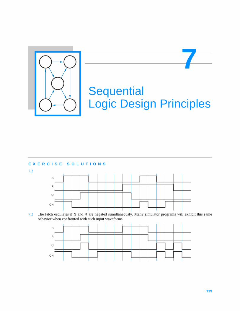
7.2
7.3 The latch oscillates if S and R are negated simultaneously. Many simulator programs will exhibit this samebehavior when confronted with such input waveforms.
S
R
Q
QN
S
R
Q
QN
120 DIGITAL CIRCUITS
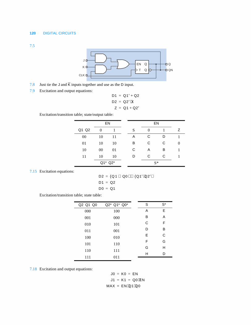
7.5
7.8 Just tie the J and K inputs together and use as the D input.
7.9 Excitation and output equations:
Excitation/transition table; state/output table:
7.15 Excitation equations:
Excitation/transition table; state table:
7.18 Excitation and output equations:
QN
QT
ENJ
K
CLK
D1 Q1 ′ Q2+=
D2 Q2 ′ X⋅=
Z Q1 Q2′+=
EN
Q1 Q2 0 1
00 10 11
01 10 10
10 00 01
11 10 10
Q1* Q2*
EN
S 0 1 Z
A C D 1
B C C 0
C A B 1
D C C 1
S*
D2 Q( 1 Q0 ) Q1′ Q2′⋅( )⊕ ⊕=
D1 Q2=
D0 Q1=
Q2 Q1 Q0 Q2* Q1* Q0*
000 100
001 000
010 101
011 001
100 010
101 110
110 111
111 011
S S*
A E
B A
C F
D B
E C
F G
G H
H D
J0 K0 EN= =
J1 K1 Q0 EN⋅= =
MAX EN Q1 Q0⋅⋅=
EXERCISE SOLUTIONS 121
Note that the characteristic equation for a J-K flip-flop is . Thus, we obtain the followingtransition equations:
Transition/output table; state/output table:
State diagram:
Timing diagram:
7.20 This can be done algebraically. If all of the input combinations are covered, the logical sum of the expressionson all the transitions leaving a state must be 1. If the sum is not 1, it is 0 for all input combinations that areuncovered. For double-covered input combinations, we look at all possible pairs of transitions leaving a state.The product of a pair of transition equations is 1 for any double-covered input combinations.
(a) State D, Y = 0 is uncovered.
(b) State A, (X+Z′) = 0 is uncovered. State B, W = 1 is double-covered; (W+X) = 0 is uncovered. State C,(W+X+Y+Z) = 0 is uncovered; (W⋅X + W⋅Y + Z⋅Y + Z⋅X) = 1 is double covered. State D, (X⋅Y + ⋅X′⋅Z + W⋅Z) = 0is uncovered; (W⋅X′⋅Z + W⋅X⋅Y⋅Z) = 1 is double-covered;
Q∗ J Q ′⋅ K ′ Q⋅+=
Q0∗ EN ′ Q0⋅ EN Q0′⋅+=
Q1∗ EN ′ Q1⋅ EN Q0⋅ Q1 ′⋅ EN Q0′ Q1⋅⋅+ +=
EN
Q1 Q2 0 1
00 00,0 01,0
01 01,0 10,0
10 10,0 11,0
11 11,0 00,1
Q1* Q2*, MAX
EN
S 0 1
A A,0 B,0
B B,0 C,0
C C,0 D,0
D D,0 A,1
S*, MAX
A
EN
EN
EN
EN′EN′
EN′EN′
EN
B
CD
CLK
EN
Q0
Q1
MAX
122 DIGITAL CIRCUITS
7.21 Table 9–4 on page 804 shows an output-coded state assignment. Here is a corresponding transition list:
The excitation equations and circuit diagram follow directly from this transition list.
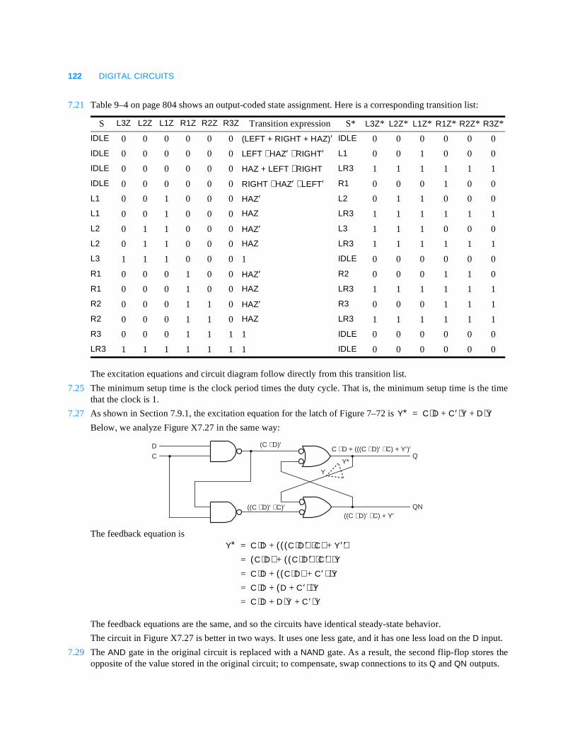
7.25 The minimum setup time is the clock period times the duty cycle. That is, the minimum setup time is the timethat the clock is 1.
7.27 As shown in Section 7.9.1, the excitation equation for the latch of Figure 7–72 is
Below, we analyze Figure X7.27 in the same way:
The feedback equation is
The feedback equations are the same, and so the circuits have identical steady-state behavior.
The circuit in Figure X7.27 is better in two ways. It uses one less gate, and it has one less load on the D input.
7.29 The AND gate in the original circuit is replaced with a NAND gate. As a result, the second flip-flop stores theopposite of the value stored in the original circuit; to compensate, swap connections to its Q and QN outputs.
S L3Z L2Z L1Z R1Z R2Z R3Z Transition expression S* L3Z* L2Z* L1Z* R1Z* R2Z* R3Z*
IDLE 0 0 0 0 0 0 (LEFT + RIGHT + HAZ)′ IDLE 0 0 0 0 0 0
IDLE 0 0 0 0 0 0 LEFT ⋅ HAZ′ ⋅ RIGHT′ L1 0 0 1 0 0 0
IDLE 0 0 0 0 0 0 HAZ + LEFT ⋅ RIGHT LR3 1 1 1 1 1 1
IDLE 0 0 0 0 0 0 RIGHT ⋅ HAZ′ ⋅ LEFT′ R1 0 0 0 1 0 0
L1 0 0 1 0 0 0 HAZ′ L2 0 1 1 0 0 0
L1 0 0 1 0 0 0 HAZ LR3 1 1 1 1 1 1
L2 0 1 1 0 0 0 HAZ′ L3 1 1 1 0 0 0
L2 0 1 1 0 0 0 HAZ LR3 1 1 1 1 1 1
L3 1 1 1 0 0 0 1 IDLE 0 0 0 0 0 0
R1 0 0 0 1 0 0 HAZ′ R2 0 0 0 1 1 0
R1 0 0 0 1 0 0 HAZ LR3 1 1 1 1 1 1
R2 0 0 0 1 1 0 HAZ′ R3 0 0 0 1 1 1
R2 0 0 0 1 1 0 HAZ LR3 1 1 1 1 1 1
R3 0 0 0 1 1 1 1 IDLE 0 0 0 0 0 0
LR3 1 1 1 1 1 1 1 IDLE 0 0 0 0 0 0
Y∗ C D⋅ C′ Y⋅ D Y⋅+ +=
D
C
(C ⋅ D)′
((C ⋅ D)′ ⋅ C) + Y′
C ⋅ D + (((C ⋅ D)′ ⋅ C) + Y′)′
((C ⋅ D)′ ⋅ C)′
Q
QN
Y∗Y
Y∗ C D⋅ C D⋅( )′ C⋅( ) Y′+( )′+=
C D⋅( ) C D⋅( )′ C⋅( )′ Y⋅+=
C D⋅ C D⋅( )( C′ ) Y⋅+ +=
C D⋅ D C ′+( ) Y⋅+=
C D⋅ D Y⋅ C ′ Y⋅+ +=
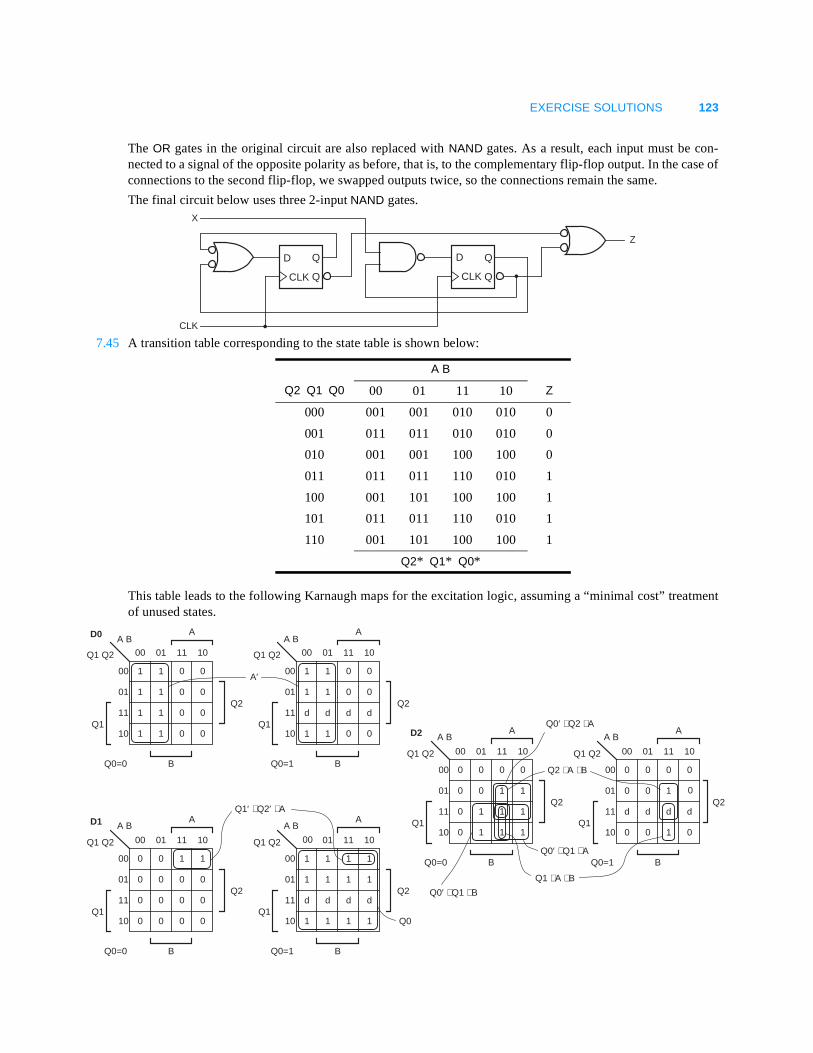
EXERCISE SOLUTIONS 123
The OR gates in the original circuit are also replaced with NAND gates. As a result, each input must be con-nected to a signal of the opposite polarity as before, that is, to the complementary flip-flop output. In the case ofconnections to the second flip-flop, we swapped outputs twice, so the connections remain the same.
The final circuit below uses three 2-input NAND gates.
7.45 A transition table corresponding to the state table is shown below:
This table leads to the following Karnaugh maps for the excitation logic, assuming a “minimal cost” treatmentof unused states.
A B
Q2 Q1 Q0 00 01 11 10 Z
000 001 001 010 010 0
001 011 011 010 010 0
010 001 001 100 100 0
011 011 011 110 010 1
100 001 101 100 100 1
101 011 011 110 010 1
110 001 101 100 100 1
Q2* Q1* Q0*
D Q
QCLK
D Q
QCLK
X
Z
CLK
00 01 11 10
00
01
11
10
00 01 11 10
A B
Q1 Q2
00
01
11
10
A
B
A BA
B
A BA
B
A BA
B
A BA
B
A BA
B
Q1
Q2
Q0=0
Q1 Q2
Q1
Q2
Q0=1
10
00
01
11
10
00 01 11 10Q1 Q2
00
01
11
10Q1
Q2
Q0=0
Q1 Q2
Q1
Q2
Q0=1
00 01 11 10
00
01
11
10
00 01 11 10Q1 Q2
00
01
11
10Q1
Q2
Q0=0
Q1 Q2
Q1
Q2
Q0=1
D0
D1
D2
1 1 0 0
1 1 0 0
1 1 0 0
1 1 0 0
0 0 1 1
0 0 0 0
0 0 0 0
0 0 0 0
1 1 0 0
0 0
0 0
1 1
1 1
1 1
1 1
1 1
1 1
0 00
0 01
0 0
0
0
0 1
0
d d d d
d d d d
d d d d
0 0 0
0 0 1 1
0 1 1 1
0 1 1 1
1 1 1 1
A′
00 11
Q1′ ⋅ Q2′ ⋅ A
Q0
Q0′ ⋅ Q1 ⋅ B
01
Q0′ ⋅ Q2 ⋅ A
Q0′ ⋅ Q1 ⋅ A
Q1 ⋅ A ⋅ B
Q2 ⋅ A ⋅ B
124 DIGITAL CIRCUITS
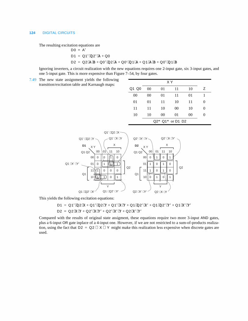
The resulting excitation equations are
Ignoring inverters, a circuit realization with the new equations requires one 2-input gate, six 3-input gates, andone 5-input gate. This is more expensive than Figure 7–54, by four gates.
7.49 The new state assignment yields the followingtransition/excitation table and Karnaugh maps:
This yields the following excitation equations:
Compared with the results of original state assigment, these equations require two more 3-input AND gates,plus a 6-input OR gate inplace of a 4-input one. However, if we are not restricted to a sum-of-products realiza-tion, using the fact that might make this realization less expensive when discrete gates areused.
D0 A′=
D1 Q1′ Q2 ′⋅ A⋅ Q0+=
D2 Q2 A⋅ B⋅ Q0 ′ Q2⋅ A⋅ Q0′ Q1⋅ A⋅ Q1 A⋅ B⋅ Q0′ Q1⋅ B⋅+ + + +=
X Y
Q1 Q0 00 01 11 10 Z
00 00 01 11 01 1
01 01 11 10 11 0
11 11 10 00 10 0
10 10 00 01 00 0
Q2* Q1* or D1 D2
00 01 10
00
01
11
10
00 01 11 10
X Y
Q1 Q2
00
01
11
10
X
Y
Q1
Q2
D1 X Y
Q1 Q2
X
Q1
Q2
D2
1
1
1 0
1
0
1
1
0
0
00
0 1
0
1
0 1 0 1
1 0 1 0
1 0 1 0
0 1 0 1
11
Y
Q1 ⋅ Q2′ ⋅ X′ Q1 ⋅ Q2′ ⋅ Y′
Q1′ ⋅ Q2 ⋅ Y Q1′ ⋅ X ⋅ Y
Q2 ⋅ X′ ⋅ Y′ Q2 ⋅ X ⋅ Y
Q2′ ⋅ X′ ⋅ Y Q2′ ⋅ X ⋅ Y′
Q1 ⋅ X′ ⋅ Y′
Q1′ ⋅ Q2 ⋅ X
D1 Q1′ Q2 X⋅ ⋅ Q1 ′ Q2 Y⋅ ⋅ Q1′ X Y⋅ ⋅ Q1 Q2′ X′⋅ ⋅ Q1 Q2 ′ Y ′⋅ ⋅ Q1 X ′ Y′⋅ ⋅+ + + + +=
D2 Q2 X Y⋅ ⋅ Q2′ X Y ′⋅ ⋅ Q2′ X′ Y Q2 X ′ Y ′⋅ ⋅+⋅ ⋅+ +=
D2 Q2 X Y⊕ ⊕=
EXERCISE SOLUTIONS 125
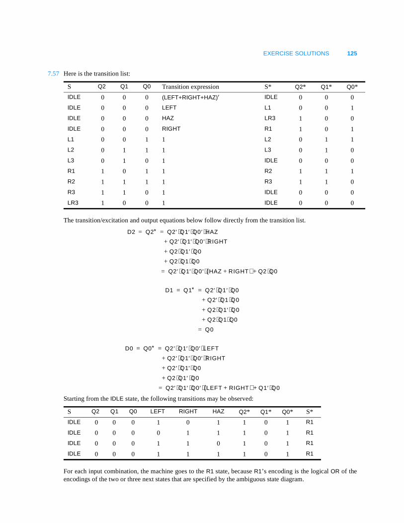
7.57 Here is the transition list:
The transition/excitation and output equations below follow directly from the transition list.
Starting from the IDLE state, the following transitions may be observed:
For each input combination, the machine goes to the R1 state, because R1’s encoding is the logical OR of theencodings of the two or three next states that are specified by the ambiguous state diagram.
S Q2 Q1 Q0 Transition expression S* Q2* Q1* Q0*
IDLE 0 0 0 (LEFT+RIGHT+HAZ)′ IDLE 0 0 0
IDLE 0 0 0 LEFT L1 0 0 1
IDLE 0 0 0 HAZ LR3 1 0 0
IDLE 0 0 0 RIGHT R1 1 0 1
L1 0 0 1 1 L2 0 1 1
L2 0 1 1 1 L3 0 1 0
L3 0 1 0 1 IDLE 0 0 0
R1 1 0 1 1 R2 1 1 1
R2 1 1 1 1 R3 1 1 0
R3 1 1 0 1 IDLE 0 0 0
LR3 1 0 0 1 IDLE 0 0 0
S Q2 Q1 Q0 LEFT RIGHT HAZ Q2* Q1* Q0* S*
IDLE 0 0 0 1 0 1 1 0 1 R1
IDLE 0 0 0 0 1 1 1 0 1 R1
IDLE 0 0 0 1 1 0 1 0 1 R1
IDLE 0 0 0 1 1 1 1 0 1 R1
D2 Q2∗ Q2′ Q1′ Q0 ′ HAZ⋅ ⋅ ⋅= =
Q2′ Q1′ Q0 ′ RIGHT⋅ ⋅ ⋅+
Q2 Q1′ Q0⋅ ⋅+
Q2 Q1 Q0⋅ ⋅+
Q2′ Q1′ Q0 ′ HAZ RIGHT+( )⋅ ⋅ ⋅ Q2 Q0⋅+=
D1 Q1∗ Q2′ Q1 ′ Q0⋅ ⋅= =
Q2′ Q1 Q0⋅ ⋅+
Q2 Q1′ Q0⋅ ⋅+
Q2 Q1 Q0⋅ ⋅+
Q0=
D0 Q0∗ Q2 ′ Q1′ Q0′ LEFT⋅ ⋅ ⋅= =
Q2 ′ Q1′ Q0′ RIGHT⋅ ⋅ ⋅+
Q2 ′ Q1′ Q0⋅ ⋅+
Q2 Q1′ Q0⋅ ⋅+
Q2′ Q1′ Q0 ′ LEFT RIGHT+( )⋅ ⋅ ⋅ Q1′ Q0⋅+=
126 DIGITAL CIRCUITS
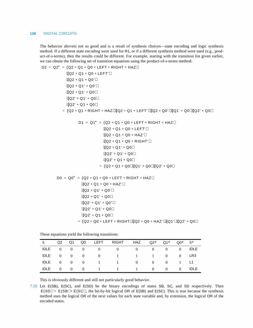
The behavior aboveis not so good and is a result of synthesis choices—state encoding and logic synthesismethod. If a different state encoding were used for R1, or if a different synthesis method were used (e.g., prod-uct-of-s-terms), then the results could be different. For example, starting with the transition list given earlier,we can obtain the following set of transition equations using the product-of-s-terms method:
These equations yield the following transitions:
This is obviously different and still not particularly good behavior.
7.58 Let E(SB), E(SC), and E(SD) be the binary encodings of states SB, SC, and SD respectively. Then, the bit-by-bit logical OR of E(SB) and E(SC). This is true because the synthesis
method uses the logical OR of the next values for each state variable and, by extension, the logical OR of theencoded states.
S Q2 Q1 Q0 LEFT RIGHT HAZ Q2* Q1* Q0* S*
IDLE 0 0 0 0 0 0 0 0 0 IDLE
IDLE 0 0 0 0 1 1 1 0 0 LR3
IDLE 0 0 0 1 1 0 0 0 1 L1
IDLE 0 0 0 1 1 1 0 0 0 IDLE
D2 Q2∗ Q2 Q1 Q0 LEFT RIGHT HAZ+ + + + +( )= =
Q2 Q1 Q0 LEFT′+ + +( )⋅ Q2 Q1 Q0′+ +( )⋅ Q2 Q1′ Q0′+ +( )⋅ Q2 Q1′ Q0+ +( )⋅ Q2′ Q1′ Q0+ +( )⋅ Q2′ Q1 Q0+ +( )⋅
Q2 Q1 RIGHT HAZ+ + +( ) Q2 Q1 LEFT′+ +( ) Q2 Q0 ′+( ) Q1′ Q0+( ) Q2′ Q0+( )⋅ ⋅ ⋅ ⋅=
D1 Q1∗ Q2 Q1 Q0 LEFT RIGHT HAZ+ + + + +( )= =
Q2 Q1 Q0 LEFT′+ + +( )⋅ Q2 Q1 Q0 HAZ′+ + +( )⋅ Q2 Q1 Q0 RIGHT′+ + +( )⋅ Q2 Q1′ Q0+ +( )⋅ Q2′ Q1′ Q0+ +( )⋅ Q2′ Q1 Q0+ +( )⋅
Q2 Q1 Q0+ +( ) Q1 ′ Q0+( ) Q2′ Q0+( )⋅ ⋅=
D0 Q0∗ Q2 Q1 Q0 LEFT RIGHT HAZ+ + + + +( )= =
Q2 Q1 Q0 HAZ′+ + +( )⋅ Q2 Q1′ Q0′+ +( )⋅ Q2 Q1′ Q0+ +( )⋅ Q2 ′ Q1 ′ Q0 ′+ +( )⋅ Q2′ Q1′ Q0+ +( )⋅ Q2′ Q1 Q0+ +( )⋅
Q2 Q0 LEFT RIGHT+ + +( ) Q2 Q0 HAZ′+ +( ) Q1′( ) Q2′ Q0+( )⋅ ⋅ ⋅=
E SD( ) E SB( ) E SC( )+=
EXERCISE SOLUTIONS 127
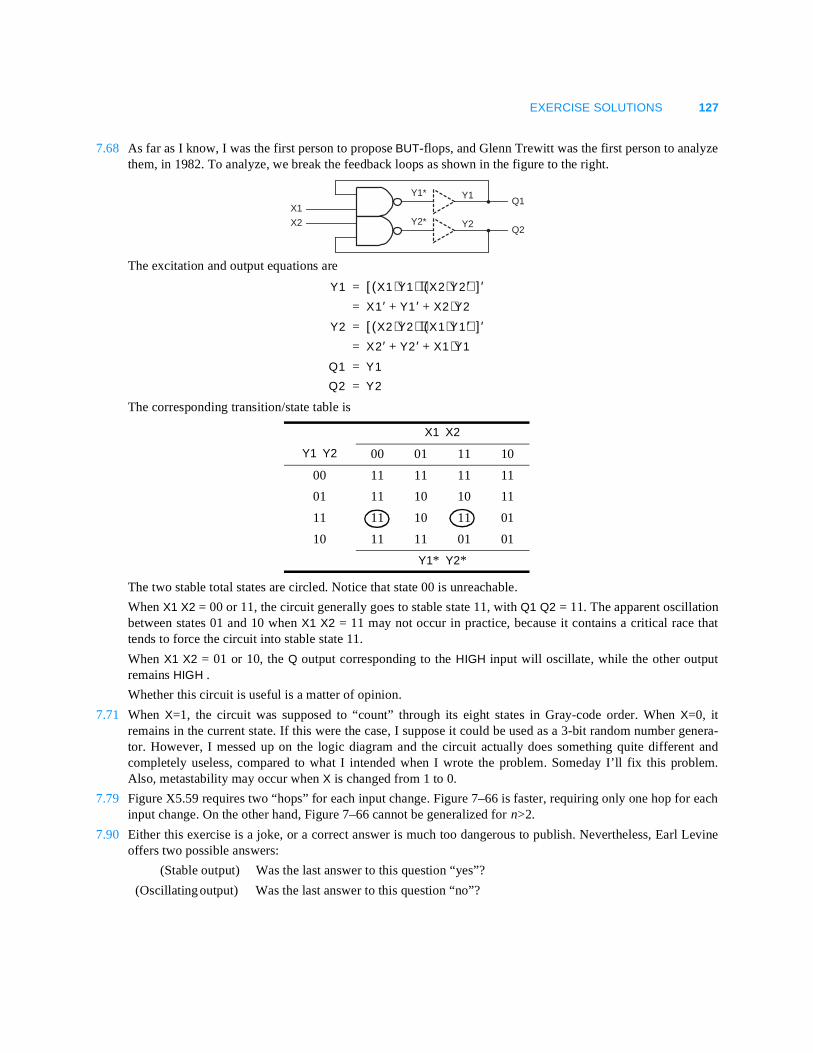
7.68 As far as I know, I was the first person to propose BUT-flops, and Glenn Trewitt was the first person to analyzethem, in 1982. To analyze, we break the feedback loops as shown in the figure to the right.
The excitation and output equations are
The corresponding transition/state table is
The two stable total states are circled. Notice that state 00 is unreachable.
When X1 X2 = 00 or 11, the circuit generally goes to stable state 11, with Q1 Q2 = 11. The apparent oscillationbetween states 01 and 10 when X1 X2 = 11 may not occur in practice, because it contains a critical race thattends to force the circuit into stable state 11.
When X1 X2 = 01 or 10, the Q output corresponding to the HIGH input will oscillate, while the other outputremains HIGH .
Whether this circuit is useful is a matter of opinion.
7.71 When X=1, the circuit was supposed to “count” through its eight states in Gray-code order. When X=0, itremains in the current state. If this were the case, I suppose it could be used as a 3-bit random number genera-tor. However, I messed up on the logic diagram and the circuit actually does something quite different andcompletely useless, compared to what I intended when I wrote the problem. Someday I’ll fix this problem.Also, metastability may occur when X is changed from 1 to 0.
7.79 Figure X5.59 requires two “hops” for each input change. Figure 7–66 is faster, requiring only one hop for eachinput change. On the other hand, Figure 7–66 cannot be generalized for n>2.
7.90 Either this exercise is a joke, or a correct answer is much too dangerous to publish. Nevertheless, Earl Levineoffers two possible answers:
(Stable output) Was the last answer to this question “yes”?
(Oscillating output) Was the last answer to this question “no”?
X2
X1Q1
Q2
Y1∗
Y2∗
Y1
Y2
Y1 X1 Y1⋅( ) X2 Y2⋅( )′⋅[ ]′=
X1′ Y1 ′ X2 Y2⋅+ +=
Y2 X2 Y2⋅( ) X1 Y1⋅( )′⋅[ ]′=
X2′ Y2 ′ X1 Y1⋅+ +=
Q1 Y1=
Q2 Y2=
X1 X2
Y1 Y2 00 01 11 10
00 11 11 11 11
01 11 10 10 11
11 11 10 11 01
10 11 11 01 01
Y1* Y2*
145
E X E R C I S E S O L U T I O N S
Sequential Logic Design Practices
874x163
CLR
CLK
LD
QA
QB
2
14
11
1
9
ENP
ENT
7
10
A
B
3
4
C
D
5
6QC
QD15
RCO
13
12
8.1 In the first three printings, change “RAMBANK0” to “RAMBANK1” in the third line of the exercise. The results arethe same. The new expression describes exactly the input combinations in which the 8 high-order bits of ABUS
are 000000012, the same as the original expression using don’t-cares.
8.2 The 16-series devices have or 2048 fuses (see Figure 10–2). The 20-series devices have or2560 fuses.
8.3 There are fuses in the AND array (see Figure 10–4). Each of the eight macrocells has one fuseto control the output polarity and one fuse to select registered vs. combinational configuration in the 16V8R, orto assert the output-enable in the 16V8S. There are also two global fuses to select the overall configuration(16V8C, 16V8R, or 16V8S). The total number of fuses is therefore .
A real 16V8 (depending on the manufacturer) has at least 64 additional fuses to disable individual productterms, 64 user-programmable fuses that do nothing but store a user code, and a security fuse. (Once the securityfuse is programmed, the rest of the fuse pattern can no longer be read.)
8.5 The column below gives the answers in MHz.
Part numbers Suffix
PAL16L8, PAL16Rx, PAL20L8, PAL20Rx -5 5 4 – 4.5 0 117.7 117.7
PAL16L8, PAL16Rx, PAL20L8, PAL20Rx -7 7.5 6.5 – 7 0 74.1 74.1
PAL16L8, PAL16Rx, PAL20L8, PAL20Rx -10 10 8 – 10 0 55.6 55.6
GAL22V10 -25 25 15 13 15 0 33.3 35.7
64 32× 64 40×
64 32× 2048=
2048 16 2+ + 2066=
fmaxE
tPD tCO tCF tSU tH fmaxE fmaxI
146 DIGITAL CIRCUITS
8.6 The column above gives the answers in MHz.
8.7module Eight_Bit_Regtitle ’8-bit Edge-Triggered Register’Z74X374 device ’P16V8R’;
" Input pinsCLK, !OE pin 1, 11; D1, D2, D3, D4, D5, D6, D7, D8 pin 2, 3, 4, 5, 6, 7, 8, 9;
" Output pins Q1, Q2, Q3, Q4, Q5, Q6, Q7, Q8 pin 19, 18, 17, 16, 15, 14, 13, 12;
" Set definitions D = [D1,D2,D3,D4,D5,D6,D7,D8]; Q = [Q1,Q2,Q3,Q4,Q5,Q6,Q7,Q8];
equations
Q := D;
end Eight_Bit_Reg
8.10 If EN or CLK is 0, the output will be stable. If both are 1, the results are unpredictable, since they depend oncircuit timing. It is certain that the circuit’s output will be unstable as long as this condition is true.
8.11 The counter is modified to return to a count of 0 when count 9 is reached.
8.13 The counting direction is controlled by QD: count up when QD=1, count down when QD=0. A load occurswhen the counter is in the terminal state, 1111 when counting up, 0000 when counting down. The MSB is com-plemented during a load and the other bits are unchanged.
Let us assume that the counter is initially in one of the states 0000–0111. Then the counter counts down(QD=0). Upon reaching state 0000, it loads 1000 and subsequently counts up (QD=1). Upon reaching state1111, the counter loads 0111, and subsequently counts down, repeating the cycle.
module Z74x162
title '4-bit Decade Counter'
"Z74X162 device 'P16V8R';
" Input pins
CLK, !OE pin 1, 11;
A, B, C, D pin 2, 3, 4, 5;
!LD, !CLR, ENP, ENT pin 6, 7, 8, 9;
" Output pins
QA, QB, QC, QD pin 19, 18, 17, 16 istype 'reg';
RCO pin 15;
" Set definitions
INPUT = [ D, C, B, A ];
COUNT = [QD, QC, QB, QA ];
equations
COUNT.CLK = CLK;
COUNT := !CLR & ( LD & INPUT
# !LD & (ENT & ENP) & (COUNT < 9) & (COUNT + 1)
# !LD & (ENT & ENP) & (COUNT == 9) & 0
# !LD & !(ENT & ENP) & COUNT);
RCO = (COUNT == 9) & ENT;
end Z74x162
fmaxI

EXERCISE SOLUTIONS 147
If the counter is initially in one of the states 1000–1111, the same cyclic behavior is observed. The countingsequence has a period of 16 and is, in decimal,
8, 9, 10, 11, 12, 13, 14, 15, 7, 6, 5, 4, 3, 2, 1, 0, 8, 9, ...
If only the three LSBs are observed, the sequence is
0, 1, 2, 3, 4, 5, 6, 7, 7, 6, 5, 4, 3, 2, 1, 0, 0, 1, ...
8.14 The only difference between a ’163 and a ’161 is that the CLR_L input of ’161 is asynchronous. Thus, thecounter will go from state 1010 to state 0000 immediately, before the next clock tick, and go from state 0000 tostate 0001 at the clock tick. Observing the state just before each clock tick, it is therefore a modulo-10 counter,with the counting sequence 0, 1, ..., 9, 0, 1, ....
Note that this type of operation is not recommended, because the width of the CLR_L pulse is not well con-trolled. That is, the NAND gate will negate the CLR_L pulse as soon as either one of its inputs goes to 0. If, say,the counter’s QB output clears quickly, and its QD output clears slowly, it is possible for CLR_L to be assertedlong enough to clear QB but not QD, resulting in an unexpected next state of 1000, or possibly metastability ofthe QD output.
8.17 The path from the Q1 counter output (B decoder input) to the Y2_L output has 10 ns more delay than the Q2 andQ0 (C and A) paths. Let us examine the possible Y2_L glitches in Figure 8–43 with this in mind:
3→4 (011→100) Because of the delay in the Q1 path, this transition will actually look like 011→110→100.The Y6_L output will have a 10-ns glitch, but Y2_L will not.
7→0 (111→000) Because of the delay in the Q1 path, this transition will actually look like 111→010→000.The Y2_L output will have a 10-ns glitch, but the others will not.
8.19 The delay calculation is different, depending on the starting state.
In the INIT state, U7 and U8 take 21 ns to propagate the CLEAR signal to the outputs. Then U6 requires 20 nssetup time on its D inputs while U3 requires 20 ns setup time on its RIN input. This implies a minimum clockperiod of 41 ns, assuming zero delay from the control unit.
In states M1–M8, the minimum clock period depends on the delay of the combinational logic in the control unitthat asserts SELSUM when MPY0 is asserted. However, the most obvious way to do this is to connect MPY0directly to SELSUM, creating a delay of 0 ns. This assumption is made below. Also, it is assumed that MPY0 is1 to find the worst case. The figure on the next page shows the worst-case path, in heavy lines, to be 106 ns.Since we would like to use the same clock for all states, the minimum clock period is 106 ns.
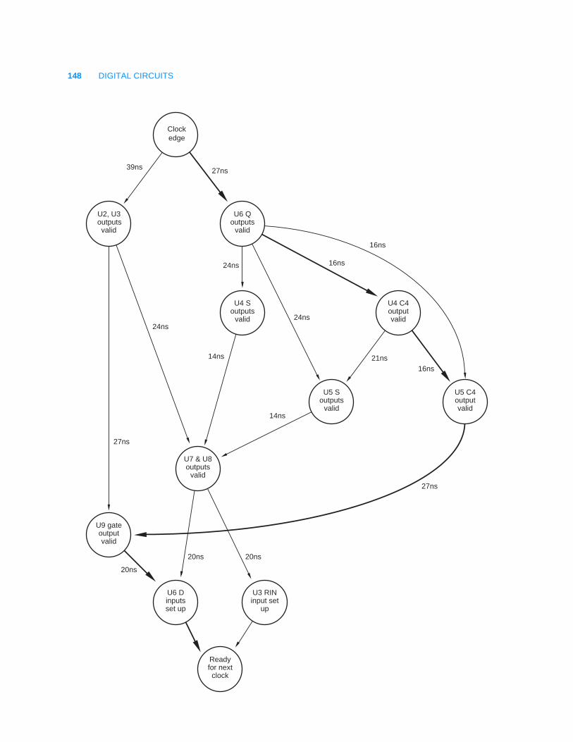
148 DIGITAL CIRCUITS
U6 Qoutputs
valid
U2, U3outputsvalid
U4 C4outputvalid
U5 C4outputvalid
U5 Soutputs
valid
U7 & U8outputs
valid
U4 Soutputs
valid
24ns
16ns21ns
16ns
16ns
24ns
27ns39ns
14ns
14ns
24ns
U9 gateoutputvalid
27ns
27ns
U6 Dinputsset up
20ns
20ns
U3 RINinput set
up
20ns
Readyfor nextclock
Clockedge
EXERCISE SOLUTIONS 149
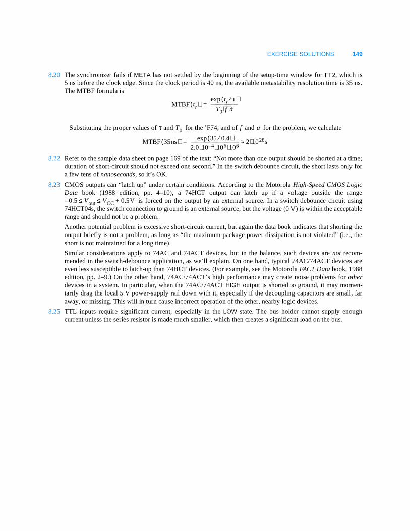
8.20 The synchronizer fails if META has not settled by the beginning of the setup-time window for FF2, which is5 ns before the clock edge. Since the clock period is 40 ns, the available metastability resolution time is 35 ns.The MTBF formula is
Substituting the proper values of and for the ’F74, and of and for the problem, we calculate
8.22 Refer to the sample data sheet on page 169 of the text: “Not more than one output should be shorted at a time;duration of short-circuit should not exceed one second.” In the switch debounce circuit, the short lasts only fora few tens of nanoseconds, so it’s OK.
8.23 CMOS outputs can “latch up” under certain conditions. According to the Motorola High-Speed CMOS LogicData book (1988 edition, pp. 4–10), a 74HCT output can latch up if a voltage outside the range
is forced on the output by an external source. In a switch debounce circuit using74HCT04s, the switch connection to ground is an external source, but the voltage (0 V) is within the acceptablerange and should not be a problem.
Another potential problem is excessive short-circuit current, but again the data book indicates that shorting theoutput briefly is not a problem, as long as “the maximum package power dissipation is not violated” (i.e., theshort is not maintained for a long time).
Similar considerations apply to 74AC and 74ACT devices, but in the balance, such devices are not recom-mended in the switch-debounce application, as we’ll explain. On one hand, typical 74AC/74ACT devices areeven less susceptible to latch-up than 74HCT devices. (For example, see the Motorola FACT Data book, 1988edition, pp. 2–9.) On the other hand, 74AC/74ACT’s high performance may create noise problems for otherdevices in a system. In particular, when the 74AC/74ACT HIGH output is shorted to ground, it may momen-tarily drag the local 5 V power-supply rail down with it, especially if the decoupling capacitors are small, faraway, or missing. This will in turn cause incorrect operation of the other, nearby logic devices.
8.25 TTL inputs require significant current, especially in the LOW state. The bus holder cannot supply enoughcurrent unless the series resistor is made much smaller, which then creates a significant load on the bus.
MTBF tr( )tr τ⁄( )exp
T0 f⋅ a⋅------------------------=
τ T0 f a
MTBF 35ns( ) 35 0.4⁄( )exp
2.0 10 4– 106 106⋅ ⋅ ⋅------------------------------------------- 2 1028s⋅≈=
0.5– Vout VCC 0.5V+≤≤
150 DIGITAL CIRCUITS
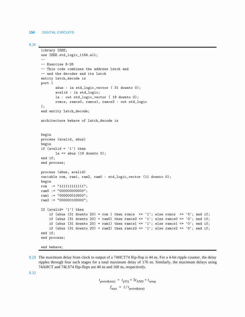
8.26 .
8.28 The maximum delay from clock to output of a 74HCT74 flip-flop is 44 ns. For a 4-bit ripple counter, the delayripples through four such stages for a total maximum delay of 176 ns. Similarly, the maximum delays using74AHCT and 74LS74 flip-flops are 40 ns and 160 ns, respectively.
8.32
library IEEE;
use IEEE.std_logic_1164.all;
--
-- Exercise 8-26
-- This code combines the address latch and
-- and the decoder and its latch
entity latch_decode is
port (
abus : in std_logic_vector ( 31 downto 0);
avalid : in std_logic;
la : out std_logic_vector ( 19 downto 0);
romcs, ramcs0, ramcs1, ramcs2 : out std_logic
);
end entity latch_decode;
architecture behave of latch_decode is
begin
process (avalid, abus)
begin
if (avalid = '1') then
la <= abus (19 downto 0);
end if;
end process;
process (abus, avalid)
variable rom, ram1, ram2, ram0 : std_logic_vector (11 downto 0);
begin
rom := "111111111111";
ram0 := "000000000000";
ram1 := "000000010000";
ram2 := "000000100000";
If (avalid= '1') then
if (abus (31 downto 20) = rom ) then romcs <= '1'; else romcs <= '0'; end if;
if (abus (31 downto 20) = ram0) then ramcs0 <= '1'; else ramcs0 <= '0'; end if;
if (abus (31 downto 20) = ram1) then ramcs1 <= '1'; else ramcs1 <= '0'; end if;
if (abus (31 downto 20) = ram2) then ramcs2 <= '1'; else ramcs2 <= '0'; end if;
end if;
end process;
end behave;
tperiod(min) tpTQ 3tAND tsetup++=
fmax 1 tperiod(min)⁄=
EXERCISE SOLUTIONS 151
8.37
Inputs Current state Next state
CLR_L LD_L ENT ENP QD QC QB QA QD∗ QC∗ QB∗ QA∗
0 x x x x x x x 0 0 0 0
1 0 x x x x x x D C B A
1 1 0 x x x x x QD QC QB QA
1 1 x 0 x x x x QD QC QB QA
1 1 1 1 0 0 0 0 0 0 0 1
1 1 1 1 0 0 0 1 0 0 1 0
1 1 1 1 0 0 1 0 0 0 1 1
1 1 1 1 0 0 1 1 0 1 0 0
1 1 1 1 0 1 0 0 0 1 0 1
1 1 1 1 0 1 0 1 0 1 1 0
1 1 1 1 0 1 1 0 0 1 1 1
1 1 1 1 0 1 1 1 1 0 0 0
1 1 1 1 1 0 0 0 1 0 0 1
1 1 1 1 1 0 0 1 0 0 0 0
1 1 1 1 1 0 1 0 1 0 1 1
1 1 1 1 1 0 1 1 0 1 0 0
1 1 1 1 1 1 0 0 1 1 0 1
1 1 1 1 1 1 0 1 0 1 0 0
1 1 1 1 1 1 1 0 1 1 1 1
1 1 1 1 1 1 1 1 0 0 0 0
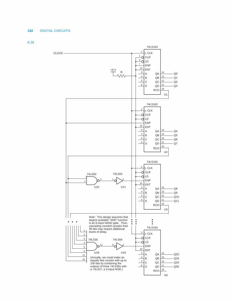
152 DIGITAL CIRCUITS
8.3874LS163
CLR
CLK
LD
QA
QB
2
14
11
1
9
ENP
ENT
7
10
A
B
3
4
C
D
5
6QC
QD15RCO
U1
13
12
74LS163
CLR
CLK
LD
QA
QB
2
14
11
ENP
ENT10
A
B
3
4
C
D
5
6QC
QD15
RCOU2
13
12
74LS163
CLR
CLK
LD
QA
QB
2
14
11
ENP
ENT10
A
B
3
4
C
D
5
6QC
QD15RCO
U3
13
12
74LS163
CLR
CLK
LD
QA
QB
2
14
11
ENP
ENT10
A
B
3
4
C
D
5
6QC
QD15RCO
U9
13
12
CLOCK
+5 VR
1
2
3
4
5
6
11
12
12 43
U18 U19
74LS30 74LS04
74LS00
U10
12
3 21
U11
74LS04
Note: This design assumes thatlargest available "AND" functionis an 8-input NAND gate. Thus,cascading counters greater than36 bits may require additionallevels of delay.
(Actually, we could make anequally fast counter with up to100 bits by combining theoutputs of three 74LS30s witha 74LS27, a 3-input NOR.)
Q0
Q1
Q2
Q3
Q4
Q5
Q6
Q7
Q8
Q9
Q10
Q11
Q32
Q33
Q34
Q35
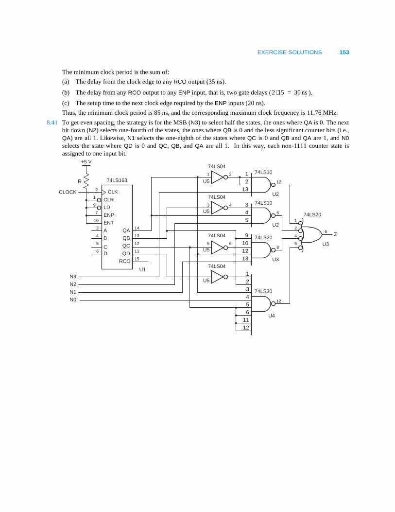
EXERCISE SOLUTIONS 153
The minimum clock period is the sum of:
(a) The delay from the clock edge to any RCO output (35 ns).
(b) The delay from any RCO output to any ENP input, that is, two gate delays ( ).
(c) The setup time to the next clock edge required by the ENP inputs (20 ns).
Thus, the minimum clock period is 85 ns, and the corresponding maximum clock frequency is 11.76 MHz.
8.41 To get even spacing, the strategy is for the MSB (N3) to select half the states, the ones where QA is 0. The nextbit down (N2) selects one-fourth of the states, the ones where QB is 0 and the less significant counter bits (i.e.,QA) are all 1. Likewise, N1 selects the one-eighth of the states where QC is 0 and QB and QA are 1, and N0selects the state where QD is 0 and QC, QB, and QA are all 1. In this way, each non-1111 counter state isassigned to one input bit.
2 15⋅ 30 ns=
14
74LS163
CLR
Z
CLK
LD
QA
N3
N2
N1
N0
QB
2
11
1
9
ENP
ENT
7
10
A
B
3
4
CD
5
6QC
QD15RCO
U1
13
12
CLOCK
+5 V
R
74LS201
2
4
5
6
U3
12 12
13U2
74LS10
34 6
5U2
74LS10
1 2
U5
74LS04
3 4
U5
U5
74LS04
5 6
74LS04
123456
1112
12
U4
74LS30
910
81213 U3
74LS20
U5
74LS04
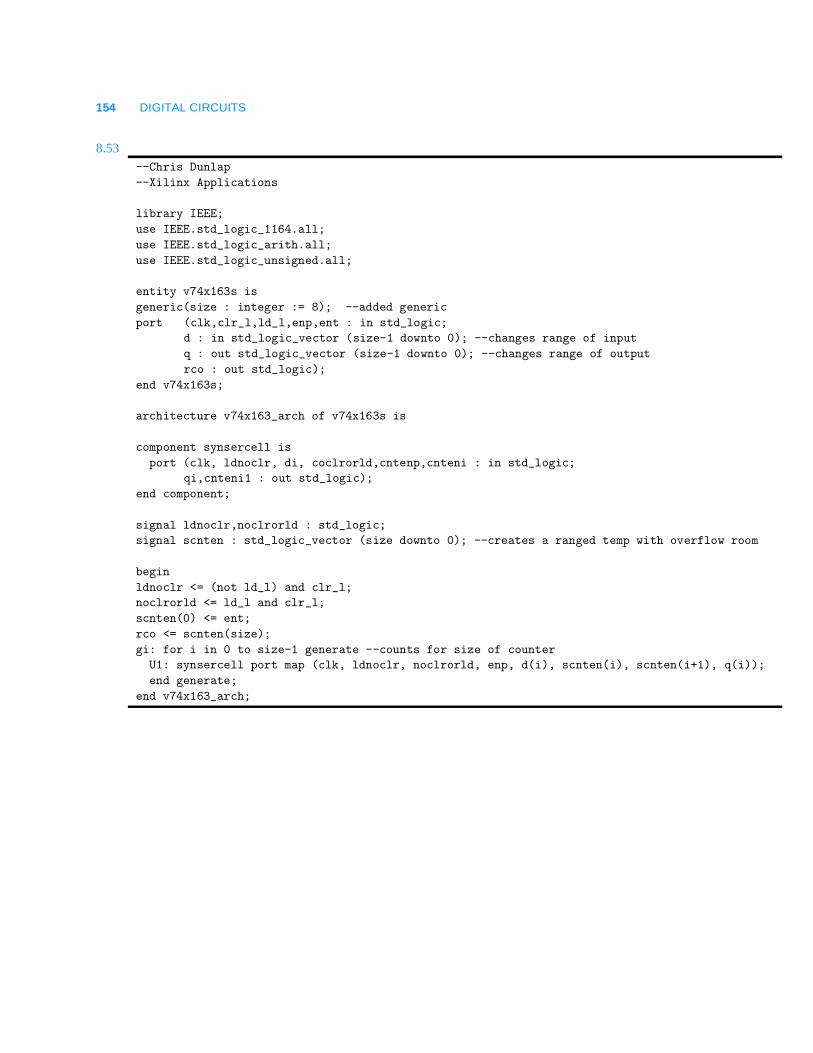
154 DIGITAL CIRCUITS
8.53--Chris Dunlap
--Xilinx Applications
library IEEE;
use IEEE.std_logic_1164.all;
use IEEE.std_logic_arith.all;
use IEEE.std_logic_unsigned.all;
entity v74x163s is
generic(size : integer := 8); --added generic
port (clk,clr_l,ld_l,enp,ent : in std_logic;
d : in std_logic_vector (size-1 downto 0); --changes range of input
q : out std_logic_vector (size-1 downto 0); --changes range of output
rco : out std_logic);
end v74x163s;
architecture v74x163_arch of v74x163s is
component synsercell is
port (clk, ldnoclr, di, coclrorld,cntenp,cnteni : in std_logic;
qi,cnteni1 : out std_logic);
end component;
signal ldnoclr,noclrorld : std_logic;
signal scnten : std_logic_vector (size downto 0); --creates a ranged temp with overflow room
begin
ldnoclr <= (not ld_l) and clr_l;
noclrorld <= ld_l and clr_l;
scnten(0) <= ent;
rco <= scnten(size);
gi: for i in 0 to size-1 generate --counts for size of counter
U1: synsercell port map (clk, ldnoclr, noclrorld, enp, d(i), scnten(i), scnten(i+1), q(i));
end generate;
end v74x163_arch;
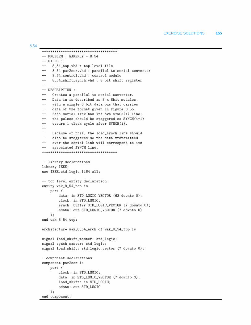
EXERCISE SOLUTIONS 155
8.54 --**********************************
-- PROBLEM : WAKERLY - 8.54
-- FILES :
-- 8_54_top.vhd : top level file
-- 8_54_par2ser.vhd : parallel to serial converter
-- 8_54_control.vhd : control module
-- 8_54_shift_synch.vhd : 8 bit shift register
--
-- DESCRIPTION :
-- Creates a parallel to serial converter.
-- Data in is described as 8 x 8bit modules,
-- with a single 8 bit data bus that carries
-- data of the format given in Figure 8-55.
-- Each serial link has its own SYNCH(i) line;
-- the pulses should be staggered so SYNCH(i+1)
-- occurs 1 clock cycle after SYNCH(i).
--
-- Because of this, the load_synch line should
-- also be staggered so the data transmitted
-- over the serial link will correspond to its
-- associated SYNCH line.
--**********************************
-- library declarations
library IEEE;
use IEEE.std_logic_1164.all;
-- top level entity declaration
entity wak_8_54_top is
port (
data: in STD_LOGIC_VECTOR (63 downto 0);
clock: in STD_LOGIC;
synch: buffer STD_LOGIC_VECTOR (7 downto 0);
sdata: out STD_LOGIC_VECTOR (7 downto 0)
);
end wak_8_54_top;
architecture wak_8_54_arch of wak_8_54_top is
signal load_shift_master: std_logic;
signal synch_master: std_logic;
signal load_shift: std_logic_vector (7 downto 0);
--component declarations
component par2ser is
port (
clock: in STD_LOGIC;
data: in STD_LOGIC_VECTOR (7 downto 0);
load_shift: in STD_LOGIC;
sdata: out STD_LOGIC
);
end component;
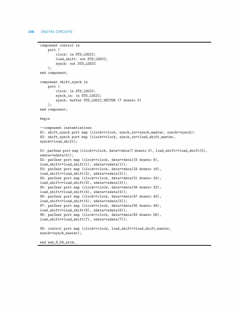
156 DIGITAL CIRCUITS
component control is
port (
clock: in STD_LOGIC;
load_shift: out STD_LOGIC;
synch: out STD_LOGIC
);
end component;
component shift_synch is
port (
clock: in STD_LOGIC;
synch_in: in STD_LOGIC;
synch: buffer STD_LOGIC_VECTOR (7 downto 0)
);
end component;
begin
--component instantiations
S1: shift_synch port map (clock=>clock, synch_in=>synch_master, synch=>synch);
S2: shift_synch port map (clock=>clock, synch_in=>load_shift_master,
synch=>load_shift);
U1: par2ser port map (clock=>clock, data=>data(7 downto 0), load_shift=>load_shift(0),
sdata=>sdata(0));
U2: par2ser port map (clock=>clock, data=>data(15 downto 8),
load_shift=>load_shift(1), sdata=>sdata(1));
U3: par2ser port map (clock=>clock, data=>data(23 downto 16),
load_shift=>load_shift(2), sdata=>sdata(2));
U4: par2ser port map (clock=>clock, data=>data(31 downto 24),
load_shift=>load_shift(3), sdata=>sdata(3));
U5: par2ser port map (clock=>clock, data=>data(39 downto 32),
load_shift=>load_shift(4), sdata=>sdata(4));
U6: par2ser port map (clock=>clock, data=>data(47 downto 40),
load_shift=>load_shift(5), sdata=>sdata(5));
U7: par2ser port map (clock=>clock, data=>data(55 downto 48),
load_shift=>load_shift(6), sdata=>sdata(6));
U8: par2ser port map (clock=>clock, data=>data(63 downto 56),
load_shift=>load_shift(7), sdata=>sdata(7));
U9: control port map (clock=>clock, load_shift=>load_shift_master,
synch=>synch_master);
end wak_8_54_arch;
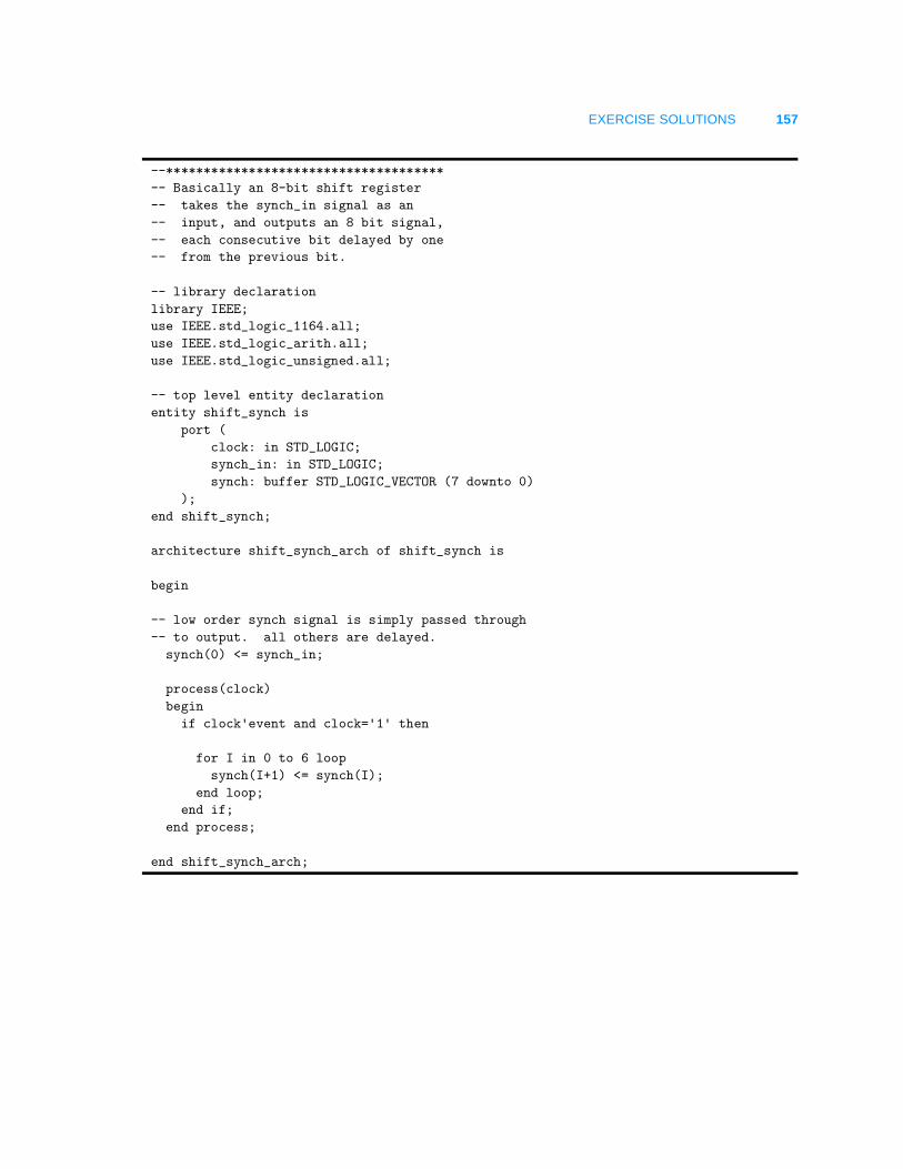
EXERCISE SOLUTIONS 157
--*************************************
-- Basically an 8-bit shift register
-- takes the synch_in signal as an
-- input, and outputs an 8 bit signal,
-- each consecutive bit delayed by one
-- from the previous bit.
-- library declaration
library IEEE;
use IEEE.std_logic_1164.all;
use IEEE.std_logic_arith.all;
use IEEE.std_logic_unsigned.all;
-- top level entity declaration
entity shift_synch is
port (
clock: in STD_LOGIC;
synch_in: in STD_LOGIC;
synch: buffer STD_LOGIC_VECTOR (7 downto 0)
);
end shift_synch;
architecture shift_synch_arch of shift_synch is
begin
-- low order synch signal is simply passed through
-- to output. all others are delayed.
synch(0) <= synch_in;
process(clock)
begin
if clock'event and clock='1' then
for I in 0 to 6 loop
synch(I+1) <= synch(I);
end loop;
end if;
end process;
end shift_synch_arch;
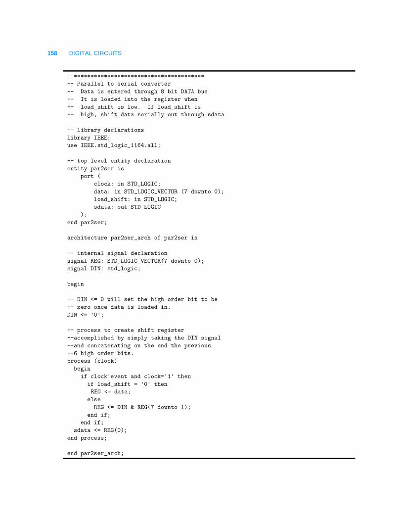
158 DIGITAL CIRCUITS
--***************************************
-- Parallel to serial converter
-- Data is entered through 8 bit DATA bus
-- It is loaded into the register when
-- load_shift is low. If load_shift is
-- high, shift data serially out through sdata
-- library declarations
library IEEE;
use IEEE.std_logic_1164.all;
-- top level entity declaration
entity par2ser is
port (
clock: in STD_LOGIC;
data: in STD_LOGIC_VECTOR (7 downto 0);
load_shift: in STD_LOGIC;
sdata: out STD_LOGIC
);
end par2ser;
architecture par2ser_arch of par2ser is
-- internal signal declaration
signal REG: STD_LOGIC_VECTOR(7 downto 0);
signal DIN: std_logic;
begin
-- DIN <= 0 will set the high order bit to be
-- zero once data is loaded in.
DIN <= '0';
-- process to create shift register
--accomplished by simply taking the DIN signal
--and concatenating on the end the previous
--6 high order bits.
process (clock)
begin
if clock'event and clock='1' then
if load_shift = '0' then
REG <= data;
else
REG <= DIN & REG(7 downto 1);
end if;
end if;
sdata <= REG(0);
end process;
end par2ser_arch;
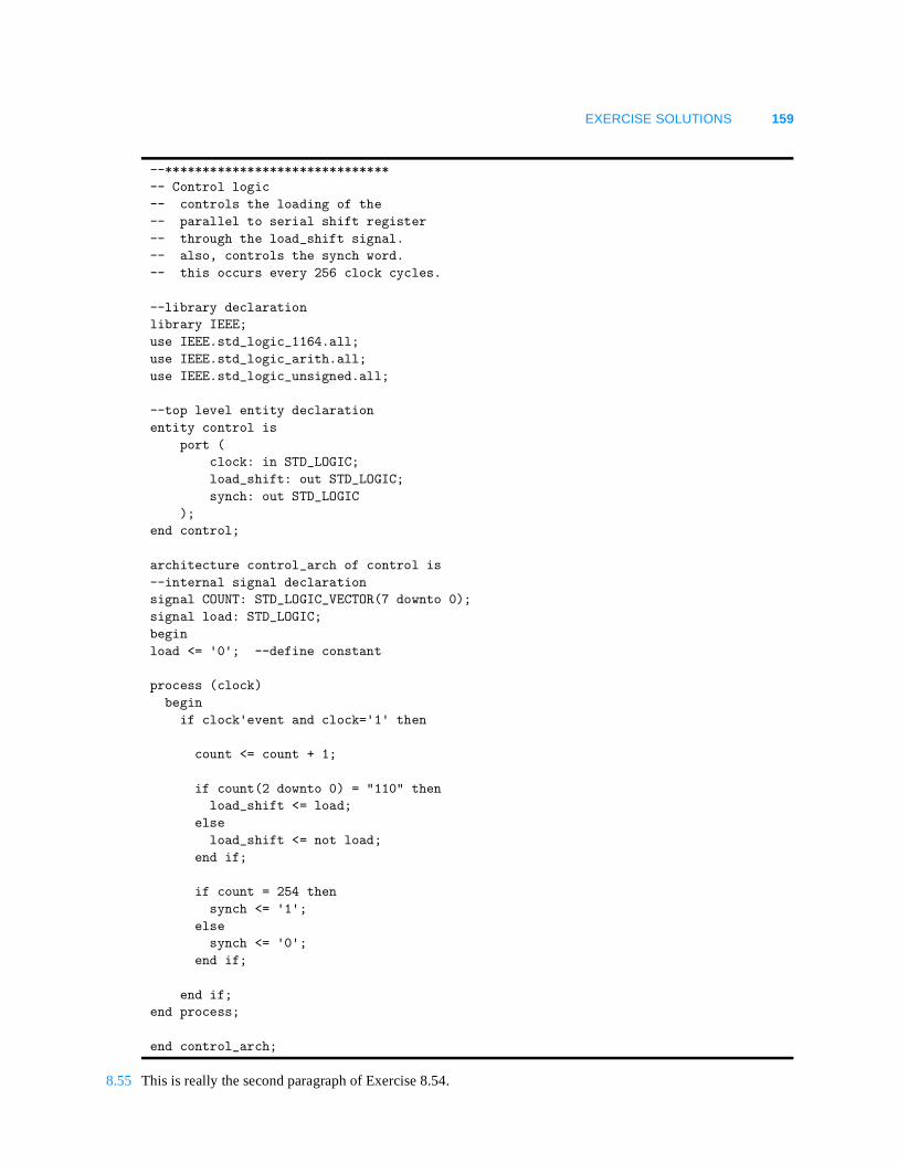
EXERCISE SOLUTIONS 159
8.55 This is really the second paragraph of Exercise 8.54.
--******************************
-- Control logic
-- controls the loading of the
-- parallel to serial shift register
-- through the load_shift signal.
-- also, controls the synch word.
-- this occurs every 256 clock cycles.
--library declaration
library IEEE;
use IEEE.std_logic_1164.all;
use IEEE.std_logic_arith.all;
use IEEE.std_logic_unsigned.all;
--top level entity declaration
entity control is
port (
clock: in STD_LOGIC;
load_shift: out STD_LOGIC;
synch: out STD_LOGIC
);
end control;
architecture control_arch of control is
--internal signal declaration
signal COUNT: STD_LOGIC_VECTOR(7 downto 0);
signal load: STD_LOGIC;
begin
load <= '0'; --define constant
process (clock)
begin
if clock'event and clock='1' then
count <= count + 1;
if count(2 downto 0) = "110" then
load_shift <= load;
else
load_shift <= not load;
end if;
if count = 254 then
synch <= '1';
else
synch <= '0';
end if;
end if;
end process;
end control_arch;
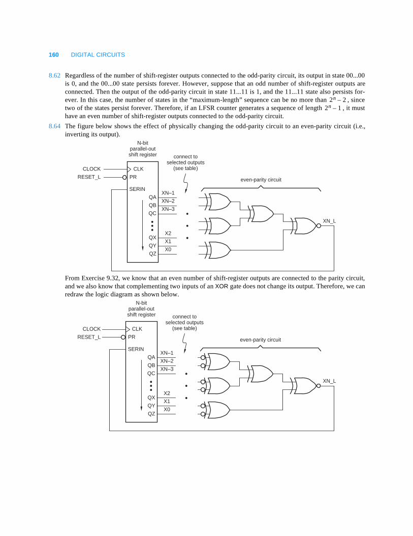
160 DIGITAL CIRCUITS
8.62 Regardless of the number of shift-register outputs connected to the odd-parity circuit, its output in state 00...00is 0, and the 00...00 state persists forever. However, suppose that an odd number of shift-register outputs areconnected. Then the output of the odd-parity circuit in state 11...11 is 1, and the 11...11 state also persists for-ever. In this case, the number of states in the “maximum-length” sequence can be no more than , sincetwo of the states persist forever. Therefore, if an LFSR counter generates a sequence of length , it musthave an even number of shift-register outputs connected to the odd-parity circuit.
8.64 The figure below shows the effect of physically changing the odd-parity circuit to an even-parity circuit (i.e.,inverting its output).
From Exercise 9.32, we know that an even number of shift-register outputs are connected to the parity circuit,and we also know that complementing two inputs of an XOR gate does not change its output. Therefore, we canredraw the logic diagram as shown below.
2n 2–2n 1–
N-bitparallel-outshift register
PR
CLK
SERIN
QB
QA
QC
QY
QX
QZ
CLOCK
RESET_L
XN_L
connect toselected outputs
(see table)
even-parity circuit
XN–1
XN–2
XN–3
X2
X1
X0
N-bitparallel-outshift register
PR
CLK
SERIN
QB
QA
QC
QY
QX
QZ
CLOCK
RESET_L
XN_L
connect toselected outputs
(see table)
even-parity circuit
XN–1
XN–2
XN–3
X2
X1
X0
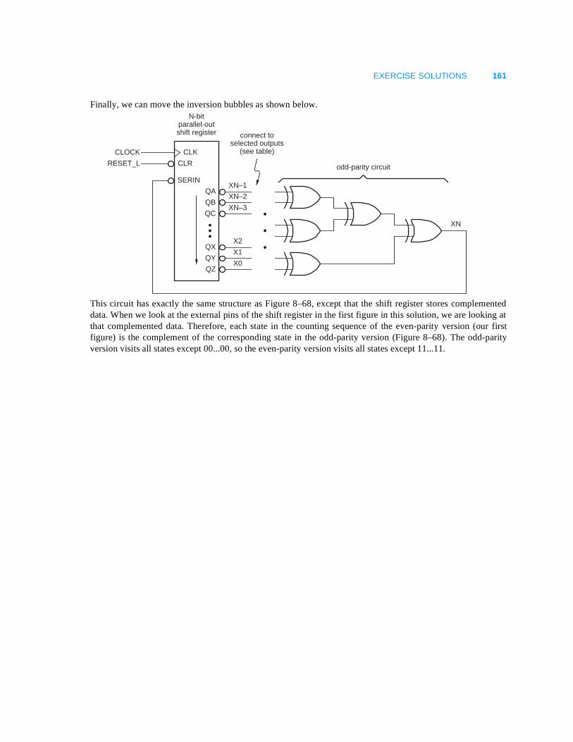
EXERCISE SOLUTIONS 161
Finally, we can move the inversion bubbles as shown below.
This circuit has exactly the same structure as Figure 8–68, except that the shift register stores complementeddata. When we look at the external pins of the shift register in the first figure in this solution, we are looking atthat complemented data. Therefore, each state in the counting sequence of the even-parity version (our firstfigure) is the complement of the corresponding state in the odd-parity version (Figure 8–68). The odd-parityversion visits all states except 00...00, so the even-parity version visits all states except 11...11.
N-bitparallel-outshift register
CLR
CLK
SERIN
QB
QA
QC
QY
QX
QZ
CLOCK
RESET_L
XN
connect toselected outputs
(see table)
odd-parity circuit
XN–1
XN–2
XN–3
X2
X1
X0
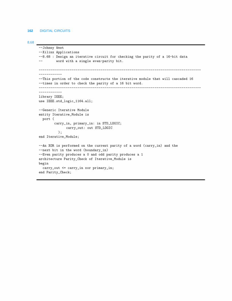
162 DIGITAL CIRCUITS
8.68 --Johnny West
--Xilinx Applications
--8.68 : Design an iterative circuit for checking the parity of a 16-bit data
-- word with a single even-parity bit.
------------------------------------------------------------------------------------
------------
--This portion of the code constructs the iterative module that will cascaded 16
--times in order to check the parity of a 16 bit word.
------------------------------------------------------------------------------------
------------
library IEEE;
use IEEE.std_logic_1164.all;
--Generic Iterative Module
entity Iterative_Module is
port (
carry_in, primary_in: in STD_LOGIC;
carry_out: out STD_LOGIC
);
end Iterative_Module;
--An XOR is performed on the current parity of a word (carry_in) and the
--next bit in the word (boundary_in)
--Even parity produces a 0 and odd parity produces a 1
architecture Parity_Check of Iterative_Module is
begin
carry_out <= carry_in xor primary_in;
end Parity_Check;
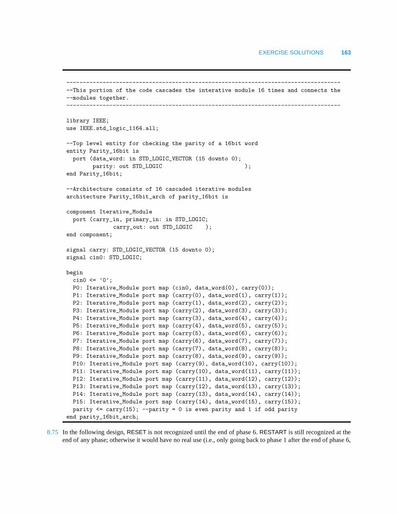
EXERCISE SOLUTIONS 163
8.75 In the following design, RESET is not recognized until the end of phase 6. RESTART is still recognized at theend of any phase; otherwise it would have no real use (i.e., only going back to phase 1 after the end of phase 6,
-----------------------------------------------------------------------------------
--This portion of the code cascades the interative module 16 times and connects the
--modules together.
-----------------------------------------------------------------------------------
library IEEE;
use IEEE.std_logic_1164.all;
--Top level entity for checking the parity of a 16bit word
entity Parity_16bit is
port (data_word: in STD_LOGIC_VECTOR (15 downto 0);
parity: out STD_LOGIC );
end Parity_16bit;
--Architecture consists of 16 cascaded iterative modules
architecture Parity_16bit_arch of parity_16bit is
component Iterative_Module
port (carry_in, primary_in: in STD_LOGIC;
carry_out: out STD_LOGIC );
end component;
signal carry: STD_LOGIC_VECTOR (15 downto 0);
signal cin0: STD_LOGIC;
begin
cin0 <= '0';
P0: Iterative_Module port map (cin0, data_word(0), carry(0));
P1: Iterative_Module port map (carry(0), data_word(1), carry(1));
P2: Iterative_Module port map (carry(1), data_word(2), carry(2));
P3: Iterative_Module port map (carry(2), data_word(3), carry(3));
P4: Iterative_Module port map (carry(3), data_word(4), carry(4));
P5: Iterative_Module port map (carry(4), data_word(5), carry(5));
P6: Iterative_Module port map (carry(5), data_word(6), carry(6));
P7: Iterative_Module port map (carry(6), data_word(7), carry(7));
P8: Iterative_Module port map (carry(7), data_word(8), carry(8));
P9: Iterative_Module port map (carry(8), data_word(9), carry(9));
P10: Iterative_Module port map (carry(9), data_word(10), carry(10));
P11: Iterative_Module port map (carry(10), data_word(11), carry(11));
P12: Iterative_Module port map (carry(11), data_word(12), carry(12));
P13: Iterative_Module port map (carry(12), data_word(13), carry(13));
P14: Iterative_Module port map (carry(13), data_word(14), carry(14));
P15: Iterative_Module port map (carry(14), data_word(15), carry(15));
parity <= carry(15); --parity = 0 is even parity and 1 if odd parity
end parity_16bit_arch;
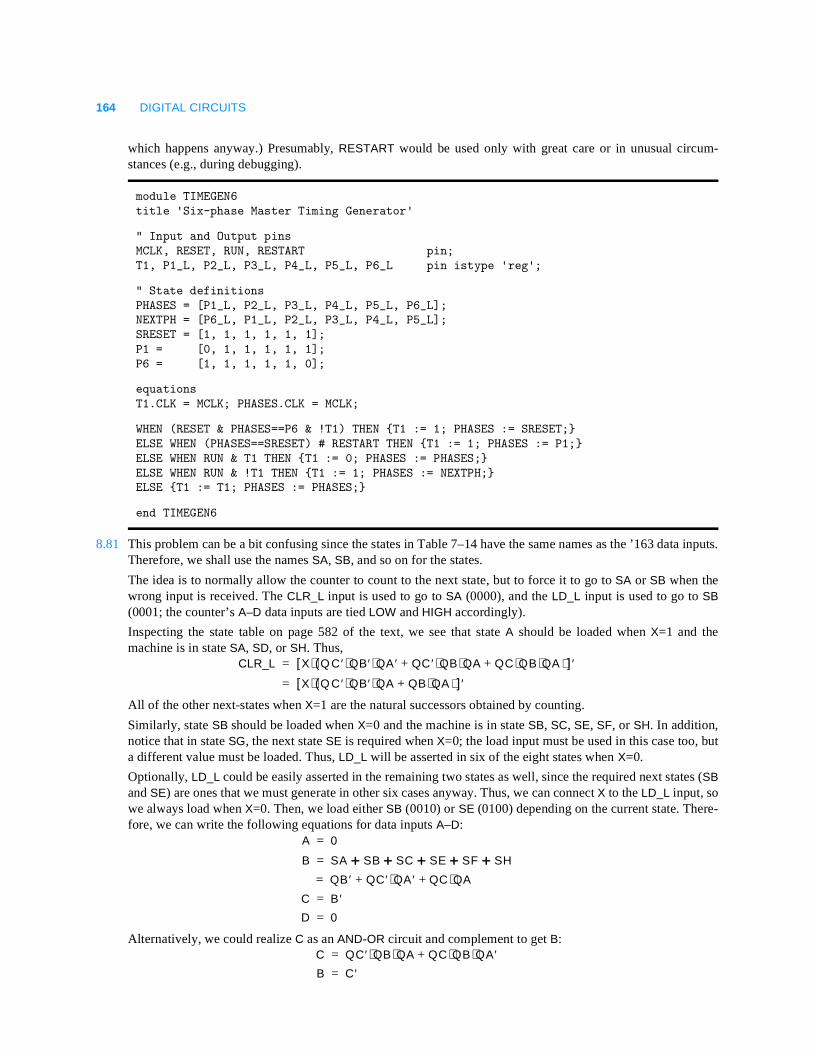
164 DIGITAL CIRCUITS
which happens anyway.) Presumably, RESTART would be used only with great care or in unusual circum-stances (e.g., during debugging).
8.81 This problem can be a bit confusing since the states in Table 7–14 have the same names as the ’163 data inputs.Therefore, we shall use the names SA, SB, and so on for the states.
The idea is to normally allow the counter to count to the next state, but to force it to go to SA or SB when thewrong input is received. The CLR_L input is used to go to SA (0000), and the LD_L input is used to go to SB(0001; the counter’s A–D data inputs are tied LOW and HIGH accordingly).
Inspecting the state table on page 582 of the text, we see that state A should be loaded when X=1 and themachine is in state SA, SD, or SH. Thus,
All of the other next-states when X=1 are the natural successors obtained by counting.
Similarly, state SB should be loaded when X=0 and the machine is in state SB, SC, SE, SF, or SH. In addition,notice that in state SG, the next state SE is required when X=0; the load input must be used in this case too, buta different value must be loaded. Thus, LD_L will be asserted in six of the eight states when X=0.
Optionally, LD_L could be easily asserted in the remaining two states as well, since the required next states (SBand SE) are ones that we must generate in other six cases anyway. Thus, we can connect X to the LD_L input, sowe always load when X=0. Then, we load either SB (0010) or SE (0100) depending on the current state. There-fore, we can write the following equations for data inputs A–D:
Alternatively, we could realize C as an AND-OR circuit and complement to get B:
module TIMEGEN6 title 'Six-phase Master Timing Generator'
" Input and Output pins MCLK, RESET, RUN, RESTART pin;T1, P1_L, P2_L, P3_L, P4_L, P5_L, P6_L pin istype 'reg';
" State definitionsPHASES = [P1_L, P2_L, P3_L, P4_L, P5_L, P6_L];NEXTPH = [P6_L, P1_L, P2_L, P3_L, P4_L, P5_L];SRESET = [1, 1, 1, 1, 1, 1];P1 = [0, 1, 1, 1, 1, 1];P6 = [1, 1, 1, 1, 1, 0];
equationsT1.CLK = MCLK; PHASES.CLK = MCLK;
WHEN (RESET & PHASES==P6 & !T1) THEN T1 := 1; PHASES := SRESET;ELSE WHEN (PHASES==SRESET) # RESTART THEN T1 := 1; PHASES := P1;ELSE WHEN RUN & T1 THEN T1 := 0; PHASES := PHASES;ELSE WHEN RUN & !T1 THEN T1 := 1; PHASES := NEXTPH;ELSE T1 := T1; PHASES := PHASES;
end TIMEGEN6
CLR_L X Q( C ′ QB′ QA ′⋅ ⋅ ⋅ QC ′ QB QA⋅ ⋅ QC QB QA )⋅ ⋅+ +[ ]′=
X Q( C ′ QB′ QA⋅ ⋅ ⋅ QB QA )⋅+[ ]′=
A 0=
B SA SB SC SE SF SH+ + + + +=
QB ′ QC′ QA ′⋅ QC QA⋅+ +=
C B ′=
D 0=
C QC′ QB QA⋅ ⋅ QC QB QA′⋅ ⋅+=
B C′=
EXERCISE SOLUTIONS 165
The logic diagram follows directly from these equations. The output logic can be realized using the equationson page 584 of the text.
8.90 Transitions on SYNCIN occur a maximum of 20 ns after the rising edge of CLOCK. Given a 40-ns clock periodand a 10-ns setup-time requirement for the other ’ALS74s, 10 ns is the maximum propagation delay of thecombinational logic.
Combinational SSI Devices
74x00
74x11
74x02
74x27
74x04 74x08
74x14 74x20
74x30
74x21
1
2
13
12
3
4
5
6
9
10
11
8
1
2
13
12
3
4
5
6
9
10
11
8
9 8
5 6
3 4
1 2
13 12
11 10
2
1
4
5
6
10
9
12
13
8
2
1
4
5
6
10
9
12
13
8
74x32
74x03
12
1311
9
108
4
56
1
23
74x10
11
1213
8
910
5
64
2
31
9 8
5 6
3 4
1 2
13 12
11 10
12
1311
9
108
4
56
1
23
12
1311
9
108
4
56
1
23
74x86
1
2
13
12
3
4
5
6
9
10
11
8
4
3
2
1
5
6
11
12
8
12
1311
9
108
4
56
1
23
12
1311
9
108
4
56
1
23
12
1311
8
910
5
64
1
23
74x266
74x138
G2A
G1
G2B
Y0
Y1
Y2
Y3
615
14
13
7
4
5
B
A
C
Y4
Y5
Y6
Y7
1
12
11
10
92
3
74x139
1A
1G
1B
1Y0
1Y1
1Y2
1Y3
1 4
5
6
7
2
3
2A
2G
2B
2Y0
2Y1
2Y2
2Y3
15 12
11
10
9
14
13
I7
I6
I5I4
I3
I2
I1
I0
A2
A1
A0
GS
EO
EI
6
7
9
14
15
10
11
12
13
1
2
3
4
5
74x14874x49
BI
A
a
b
3 11
10
c9
d8
e6
f13
g12
5
B
C
1
2
D4
74x85
5
7
9
A<B
A=B
A>B
12
11
13
14
A=B
A<B
A>B
A0
B0
A1
B1
A2
B2
A3
B3
3
2
4
10
15
1
6
74x153
1G
1C0
1C1
1C2
1C3
2C0
2C1
2C2
2C3
A
1
71Y
92Y
6
5
4
3
15
10
11
12
13
B2
14
2G
74x155
1G
1C
2C
A
2
92Y0
102Y1
112Y2
122Y3
71Y0
61Y1
51Y2
41Y3
1
14
15
B3
13
2G
74x157
1A
1B
2A
2B
3A
3B
4A
4B
G
24
1Y
72Y
93Y
124Y
3
5
6
11
10
14
13
S1
15
74x181
CIN2 9
F01
23
22
S3
S2
S1
B1
A0
B0
A1
4
3
5
7
19
18
21
20
B3
A2
B2
A3
S06
M8
15P
17G
10F1
11F2
13F3
16COUT
14A=B
74x182
2
12C1
14
15
5
6
C0
G0
P0
G1
P1
G2
P2
G3
P3
3
13
4
1
11C2
9C3
10G
P7
74x240
2G
1G
1Y1
1Y2
1Y3
1
19
12
9
14
16
18
7
1A1
1A2
1A3
1A4
2A1
2A2
2A3
2A4
1Y4
2Y1
2Y2
2Y3
2Y4
2
5
3
4
6
8
11
13
15
17
74x241
2G
1G
1Y1
1Y2
1Y3
1
19
12
9
14
16
18
7
1A1
1A2
1A3
1A4
2A1
2A2
2A3
2A4
1Y4
2Y1
2Y2
2Y3
2Y4
2
5
3
4
6
8
11
13
15
17
74x245
DIR
G
B1
B2
B3
19
1
15
14
16
17
18
13
A1
A2
A3
A4
A5
A6
A7
A8
B4
B5
B6
B7
B8
2
12
11
3
4
5
6
7
8
9
74x251
D0
D1
D2
D3
D4
D5
D6
D7
EN
4
6
5Y
Y3
2
1
15
14
13
12
A
B
C
11
10
9
7
74x253
1EN
1C0
1C1
1C2
1C3
2C0
2C1
2C2
2C3
A
1
71Y
92Y
6
5
4
3
15
10
11
12
13
B2
14
2EN
74x257
1A
1B
2A
2B
3A
3B
4A
4B
EN
24
1Y
72Y
93Y
124Y
3
5
6
11
10
14
13
S1
15
74x280
D
E
F
G
H
I
12
5EVEN
ODD13
1
2
4
A
B
C
9
8
10
11
6
74x283
A0
C0
B0
S0
S1
7
4
10
5
6
A1
B1
3
2
A2
B2
14
15
A3
B3
12
11
S2
S3
9C4
1
13
74x381
CIN3 8
F04
1
2
S0
S1
S2
B1
A0
B0
A1
6
5
7
15
19
18
17
16B3
A2
B2
A3
14P
13G
9F1
11F2
12F3
74x382
CIN3 8
F04
1
2
S0
S1
S2
B1
A0
B0
A1
6
5
7
15
19
18
17
16B3
A2
B2
A3
14COUT
13OVR
9F1
11F2
12F3
74x540
G2
G1
Y1
Y2
Y3
1
19
15
14
16
17
18
13
A1
A2
A3
A4
A5
A6
A7
A8
Y4
Y5
Y6
Y7
Y8
2
12
11
3
4
5
6
7
8
9
74x541
G2
G1
Y1
Y2
Y3
1
19
15
14
16
17
18
13
A1
A2
A3
A4
A5
A6
A7
A8
Y4
Y5
Y6
Y7
Y8
2
12
11
3
4
5
6
7
8
9
74x682
P=Q
P>Q
P0
19
1
Q0
P1
Q1
P2
Q2
P3
Q3
P4
Q4
P5
Q5
P6
Q6
P7
Q7
2
3
4
5
6
7
8
9
11
12
13
14
15
16
17
18
Combinational MSI Devices74x151
4
3
2
1
15
14
13
12
D0
D1
D2
D3
D4
D5
D6
D7
EN
6
5Y
Y
A
B
C
11
10
9
7
15
14
11
3
2
1
PAL16L8
I1
O1
IO2
IO3
IO4
IO5
IO6
IO7
O8
I2
I3
I4
I5
I6
I7
I8
I9
I10
19
18
17
16
13
12
4
5
6
7
8
9
GAL16V8C
15
14
11
3
2
1I1
O1
IO2
IO3
IO4
IO5
IO6
IO7
O8
I2
I3
I4
I5
I6
I7
I8
I9
I10
19
18
17
16
13
12
4
5
6
7
8
9
15
14
11
3
2
1CLK
PAL16R4
I1 IO1
IO2
O3
O4
O5
O6
IO7
IO8
I2
I3
I4
I5
I6
I7
I8OE
19
18
17
16
13
12
4
5
6
7
8
9
15
14
11
3
2
1CLK
GAL16V8R
I1 IO1
IO2
IO3
IO4
IO5
IO6
IO7
IO8
I2
I3
I4
I5
I6
I7
I8OE
19
18
17
16
13
12
4
5
6
7
8
9
15
14
11
3
2
1CLK
PAL16R6
I1 IO1
O2
O3
O4
O5
O6
O7
IO8
I2
I3
I4
I5
I6
I7
I8OE
19
18
17
16
13
12
4
5
6
7
8
9
15
14
11
3
2
1CLK
PAL16R8
I1 O1
O2
O3
O4
O5
O6
O7O8
I2
I3
I4
I5
I6
I7I8
OE
19
18
17
16
13
12
4
5
6
7
8
9
6
7
8
9
21
20
10
3
2
23
PAL20R8
I1
O1
O2
O3
O4
O5
O6
O7
O8
I2
I3
I4
I5
I6
I7
I8
I9
I1011
I1114
I12
19
18
17
22
16
15
4
5
13
1CLK
OE
21
20
3
2
PAL20R6
I1
IO1
O2
O3
O4
O5
O6
O7
IO8
I2
I3
I4
19
18
17
22
16
15
4
5
1CLK
6
7
8
9
10
23
I5
I6
I7
I8
I9
I1011
I1114
I1213
OE
21
20
3
2
1
PAL20L8
I1
O1
IO2
IO3
IO4
IO5
IO6
IO7
O8
I2
I3
I4
I5
I6
I7
I8
I9
I10
I11
I12
I13
I14
19
18
17
22
16
15
4
5
6
7
8
9
10
23
11
14
13
GAL20V8C
21
20
3
2
1I1
O1
IO2
IO3
IO4
IO5
IO6
IO7
O8
I2
I3
I4
I5
I6
I7
I8
I9
I10
I11
I12
I13
I14
19
18
17
22
16
15
4
5
6
7
8
9
10
23
11
14
13
21
20
3
2
PAL20R4
I1
IO1
IO2
O3
O4
O5
O6
IO7
IO8
I2
I3
I4
19
18
17
22
16
15
4
5
1CLK
6
7
8
9
10
23
I5
I6
I7
I8
I9
I1011
I1114
I1213
OE
21
20
3
2
GAL20V8R
I1
IO1
IO2
IO3
IO4
IO5
IO6
IO7
IO8
I2
I3
I4
19
18
17
22
16
15
4
5
1CLK
6
7
8
9
10
23
I5
I6
I7
I8
I9
I1011
I1114
I1213
OE
21
20
3
2
GAL22V10
IO1
IO2
IO3
IO4
IO5
IO6
IO7
IO8
IO9
IO10
I2
I3
I4
19
18
17
22
23
16
15
14
4
5
1CLK/I1
6
7
8
9
10
I5
I6
I7
I8
I9
I1011
I1113
I12
22
21
19
3
2
PAL20L10
I1
O1
IO2
IO3
IO4
IO5
IO6
IO7
IO8
I2
I3
I420
18
17
23
16
15IO9
O1014
4
5
1
6
7
8
9
10
I5
I6
I7
I8
I9
I10
I11
I12
11
13
22
21
19
3
2
PAL20X4
I1 IO1
IO2
IO3
O4
O5
O6
O7
IO8
I2
I3
I420
18
17
23
16
15IO9
IO1014
4
5
1CLK
6
7
8
9
10
I5
I6
I7
I8
I9
I1011
13OE
22
21
19
3
2
PAL20X8
I1 IO1
O2
O3
O4
O5
O6
O7
O8
I2
I3
I420
18
17
23
16
15O9
IO1014
4
5
1CLK
6
7
8
9
10
I5
I6
I7
I8
I9
I1011
13OE
22
21
19
3
2
PAL20X10
I1 O1
O2
O3
O4
O5
O6
O7
O8
I2
I3
I420
18
17
23
16
15O9
O1014
4
5
1CLK
6
7
8
9
10
I5
I6
I7
I8
I9
I1011
13OE
3
15
4
14
5
4164
DOUT
A0
A1
A2
7
6
12
11
10
13
9
A3
A4
A5
A6
A7
DIN2
RAS
CAS
WE3
15
4
5
4256
DOUT
A0
A1
A2
14
7
6
12
11
10
13
9
A3
A4
A5
A6
A7
A81
DIN2
RAS
CAS
WE
RAS
CAS
WE
OE
3
15
13
4464
DIO2
DIO1
DIO3
DIO4
A0
A1
A2
17
2
12
11
14
8
7
6
10
1
A3
A4
A5
A6
A7
16
5
4
2
16
3
5
41000
DOUT
A0
A1
A2
17
6
7
8
10
11
12
13
A3
A4
A5
A6
A7
A814
DIN
A915
1
RAS
CAS
WE
2
18
7
44256
DIO2
DIO1
DIO3
DIO4
A0
A1
A2
19
1
8
9
6
11
12
13
14
17
4
15
A3
A4
A5
A6
A7
A8
3
16
CAS
WE
OE
RAS
Static RAMs
Dynamic RAMs
20X-Series 24-pin Bipolar PLDs
CMOS GAL Devices
16R-Series 20-pin Bipolar PLDs 20R-Series24-pin Bipolar PLDs
19
22
26
20
27
12
13
10
HM6264
IO1
IO0
IO2
IO3
IO4
IO5
IO6
IO7
A0
A1
A2
15
16
11
17
18
9
8
7
6
5
4
3
21
23
A3
A4
A5
A6
A7
A825
A924
A10
2A11
A12
WE
CS1
CS2
OE
19
22
20
1
12
13
10
HM62256
IO1
IO0
IO2
IO3
IO4
IO5
IO6
IO7
A0
A1
A2
15
16
11
17
18
9
8
7
6
5
4
3
21
27
A3
A4
A5
A6
A7
A825
A924
A10
26
2A12
A13
A14
WE
CS
OE
23A11