Embed Size (px)
Citation preview

Dejan [email protected]
Introduction
EE219A – Spring 2008Special Topics in Circuits and Signal Processing
Lecture 1
Slide 2EE219A – Spring 2008 Lecture 1
What is This Course About?
CircuitOptimization
Signal Proc. Architectures
AlgorithmModeling
Simulink/XSG Model- bit-true cycle-accurate- hw-equivalent blocks- target: FPGA or ASIC
Min Energy & Area- interleaving, folding- iterative sqrt/div- loop retiming
Opt Energy-Delay- parallelism, time-mux- circuit topology- Vdd, Vth, gate size
Complex DSP
topology A
topology B
Delay
Ener
gy
c
zm ba
x2xN
time indexk
y1 y2 yN
k-1
zN z2z1
k-a/N
a+b+m=N
time index
x1
N*fClk

Slide 3EE219A – Spring 2008 Lecture 1
Course Objectives
The implementation of signal processing systems in CMOS technology– A design methodology starting from a high level
description through to an implementation optimized for hardware constraints
To understand the issues involved in the design of signal processing systems– Wireless systems will be used as a main design driver
to understand how to make tradeoffs in signal processing implementation
Slide 4EE219A – Spring 2008 Lecture 1
Background
Familiarity with basic digital ICs, VLSI design, signal processing and communications
Slide 5EE219A – Spring 2008 Lecture 1
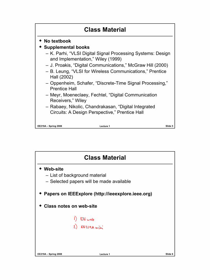
Class Material
No textbookSupplemental books– K. Parhi, “VLSI Digital Signal Processing Systems: Design
and Implementation,” Wiley (1999)– J. Proakis, “Digital Communications,” McGraw Hill (2000)– B. Leung, “VLSI for Wireless Communications,” Prentice
Hall (2002)– Oppenheim, Schafer, “Discrete-Time Signal Processing,”
Prentice Hall– Meyr, Moeneclaey, Fechtel, “Digital Communication
Receivers,” Wiley– Rabaey, Nikolic, Chandrakasan, “Digital Integrated
Circuits: A Design Perspective,” Prentice Hall
Slide 6EE219A – Spring 2008 Lecture 1
Class Material
Web-site– List of background material– Selected papers will be made available
Papers on IEEExplore (http://ieeexplore.ieee.org)
Class notes on web-site

Slide 7EE219A – Spring 2008 Lecture 1
Class Topics
The course aims to convey a knowledge of advanced concepts in VLSI signal processing. Emphasis is on the architectural exploration, design, and optimization of signal processing systems for communications and other emerging applications.
Special focus in Spring 2008– Wireless receivers
● OFDM, Software-defined radio● MIMO decoders
– Neural signal processing
Slide 8EE219A – Spring 2008 Lecture 1
Class Topics
Fundamentals– Principles of VLSI signal processing– Concurrency, pipelining, scheduling
Arithmetic for DSPTools: Matlab/Simulink, Synplify DSP, FPGA hardwareBuilding blocks– LMS, adaptive equalizers– DFE, Viterbi
Systems– Wireless, OFDM, MIMO– Neural

Slide 9EE219A – Spring 2008 Lecture 1
Design Trajectory: From DSP Theory…
Digital Signal Processing
Harry Nyquist Alan Oppenheim Jean Baptiste Fourier
Sample &Quantize
AudioVideoRadar
AddMultiplyMemory
Slide 10EE219A – Spring 2008 Lecture 1
Design, Optimization, and Verification in Matlab/Simulink environment
ASIC
FPGA
Micro Arch.
E
Circuit
E
Macro Arch.
E & A D
E
A
EN
tr.per
in outy
A Zy [4x1]
r [4x4]
y [4x4]
ky [4x1]
A Z
RY
y
r [4x4]
U [4x4]
Sigma
W [4x4]
PE U-Sigma
A Z
KY
12,9 10,8
14,9
8,5
…to Optimized Hardware Realization
Automated environment for optimal hardwaredesign and verification
optimization hardware design I/O verification
Slide 11EE219A – Spring 2008 Lecture 1
Proposed Approach
Algorithm characteristic evaluationArchitectural implementation estimationFast and predictable implementation path
Architecture
Algorithm
Digital SignalProcessor Reconfigurable
Hardware
DedicatedHardware
Establish an integrated design framework that enables efficient and effective algorithm and architecture exploration.
Slide 12EE219A – Spring 2008 Lecture 1
Class Organization
3-4 homework assignments
1 term-long design project– Phase 1: proposal (by week 5)– Phase 2: architectural study (by week 7)– Phase 3: system design & FPGA implementation
(by week 10)– Presentation and report by final week
Software training (Synplicity)– Sometime around week 5 (TBD)
Midterm

Slide 13EE219A – Spring 2008 Lecture 1
EE219A Weekly Schedule
ProblemSets Due
Mon
Tue
Wed
Thu
Fri
Lec5419 BH
Lec5419 BH
9 10 11 12 1 2 3 4 5 6 7OH
56-147EEng-4
OH56-147EEng-4
Instructor Info:Dejan Markovic56-147E [email protected]: 825-8656
Slide 14EE219A – Spring 2008 Lecture 1
Grading Policy and Timeline
Homeworks: 25%Midterm: 20%Final Project: 50%Participation: 5%
1 2 3 4 5 6 7 8 9 10Week
Class project
Phase-1 Presentation
h1 h2 h4homeworks
SynplicityTraining
TBD
Phase-2
h3
MidtermWed, May 14
Slide 15EE219A – Spring 2008 Lecture 1
Homework and Projects
Approximately 4 homeworks that will implement individual DSP blocks
In-class presentations (review of research papers)
A final project will be to put a complete system together and demonstrate it on FPGA
Slide 16EE219A – Spring 2008 Lecture 1
General Project Topic Areas
Wireless baseband signal processing– Dedicated (single-standard)– Flexible (software defined / cognitive radio)
Iterative decoders for wireless– MIMO decoders, LDPC decoders
Neural signal processing– Spike sorting
EDA infrastructure– Wordlength optimization

Slide 17EE219A – Spring 2008 Lecture 1
Some Specific Inputs (More Coming)
CRC generator/checker for Ethernet / IEEE 802.3– Cisco
OFDMA receiver/transmitter– Qualcomm
System examples from Synplicity– Simple DSP kernels (filters, encoders, …)– Systems, e.g. IEEE 802.11a receiver/transmitter
Slide 18EE219A – Spring 2008 Lecture 1
Timed dataflow
DSP algorithm
SysGen SynDSP
B-box HDL
FPGAbackend
ASICbackend
ArchitecturalTransformations
SpeedPowerArea
Hardwareco-simulation
EE219A Design Flow
Slide 19EE219A – Spring 2008 Lecture 1
Algorithmdescription
(Matlab/Simulink)
FPGA hardware emulation
(XUP, BEE2)
Chip synthesisRetiming, P&R
(Cadence)
Circuit designintroductory(Cadence)
Circuit designadvanced(Cadence)
Architecturetransformations(Simulink/C++)
RTL description
219A
216A219A215B215E
115A115B115C
216A215B215A215E
219ADSP +Com.
219ADSP +Com.
Windows/Linux
Windows
Windows/Linux
Linux
Linux Linux
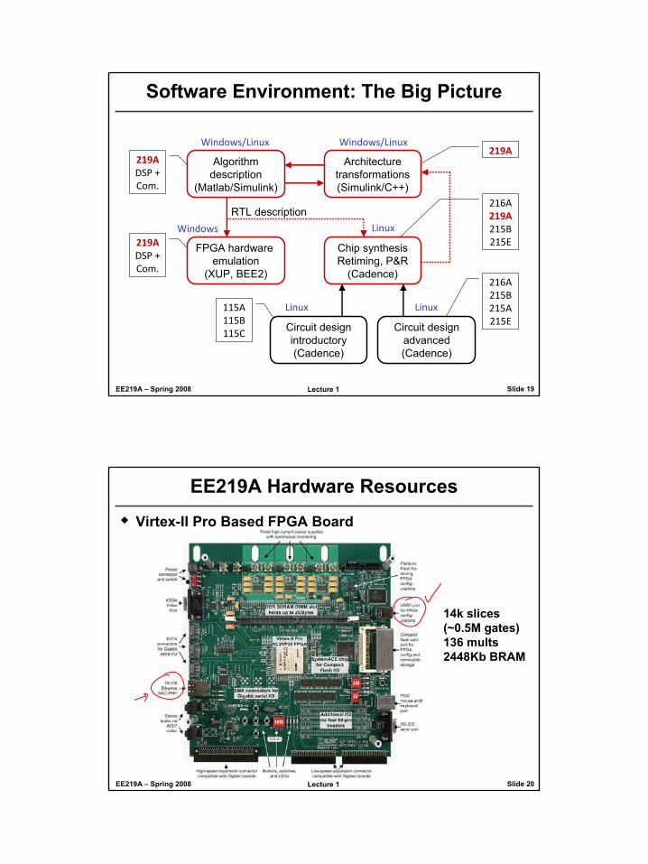
Software Environment: The Big Picture
Slide 20EE219A – Spring 2008 Lecture 1
EE219A Hardware Resources
Virtex-II Pro Based FPGA Board
14k slices(~0.5M gates)136 mults2448Kb BRAM

Slide 21EE219A – Spring 2008 Lecture 1
Real-time DSP:• 4 FPGAs ~ 10 M gates (250 MHz)• Embedded processors: PPC+ARM• On-chip memory: > 10 Mbits• Dynamic Partial Reconfiguration• Dedicated blocks: 18b mult + MAC• Architecture optimization for ASIC
• Parallelism/Pipelining/Interleaving• Wordlength optimization
Real-time Protocol Processor:• Central FPGA: PowerPC+Linux• On-chip Ethernet MAC• Bus connection to 4 other FPGAs
Radio interfaces:• 16 x 10 Gbps Infiniband• 4 interfaces per FPGA• Fiber optic cable compatible
EE219A Hardware Resources
OS-enabled multi-FPGA platform (BEE2)
Slide 22EE219A – Spring 2008 Lecture 1
Basic Problem
There is a missing link between algorithm developers and hardware designers
Algorithm designers Chip designers
Gate delay, leakage powernumber of bits, latency?
Shannon limit, Raleigh fading,cyclostationary process ? ^$*#^$E(W^$^&$
^$*#^$E(W^$^&$
“Results”– Very constrained implementation choices– Design reentry (Matlab/C, HDL)

Slide 23EE219A – Spring 2008 Lecture 1
Proposed ApproachUnified Simulink environment– Enter design only once!– Algorithm verification / emulation– Abstract view of architecture– FPGA based ASIC debug
Hardware-equivalent blocks– Basic operators
● Add, multiply, shift, mux…– Implementation constraints
● Word-size, latency
Slide 24EE219A – Spring 2008 Lecture 1
Hardware Libraries
Xilinx System Generator Synplify DSP

Slide 25EE219A – Spring 2008 Lecture 1
Complete Synplify DSP Library
FFTTransforms
DivExpLogPolarRotatorSinCosSqrt
CORDIC
CICDifferentiatorFIRFIR Rate ConverterIIRIntegratorFIR Engine (Adaptive)Reloadable FIR
Filtering
DelayFIFOPermutationRAMRegisterROMShift Register
Memories
AbsAccumulatorAddBinary LogicComparatorDivModGainInverterLog (ln,log10,log2)MinMaxMultNegatePowShifterSignSinCosSqrt
MathConcatenateConvertDe/CommutatorDe/MuxDown/UpsampleExtractParallel to SerialRecastSerial to ParallelVector De/Mux
Signal Operations
ConstantCounterDDS (NCO)RampRandomSequence
Sources
M ControlMealy State MachineMoore State Machine
Control LogicBlack BoxSubsystems
Block De/InterleaverConvolutionalDe/InterleaverConvolutional EncoderDe/PunctureViterbi Decoder
Communications
Synplify DSP v3.2
New!
New!
[Courtesy: Synplicity]
Slide 26EE219A – Spring 2008 Lecture 1
Synplify DSP Library Features
HW ImplementableSimulink BlocksetFeatures:– Datapath Propagation– Sample Rate Display– Fixed-Point Analysis– Fast Simulation:
Simulink S-Functions– Hardware Abstraction
Automatic Propagation of Fixed-Point Quantization Parameters
Automatic Propagation of Fixed-Point Quantization Parameters
Analyze and Debug Quantization Effects with Fixed-Point System Tools
Analyze and Debug Quantization Effects with Fixed-Point System Tools
Full User Control of Precision
Full User Control of Precision
Automatic Propagation and Display of Sample Rate Relationships
Automatic Propagation and Display of Sample Rate Relationships
[Courtesy: Synplicity]

Slide 27EE219A – Spring 2008 Lecture 1
XSG Model Example: Iterative 1/sqrt()
User defined parameters:- data type- wordlength (#bits, binary pt)- quantization- overflow- latency- sample period
wordlength
latency
xs(k+1) = xs(k) / 2· (3–Z· xs
2(k))
User defined parameters– Data type– Wordlength (#bits, binary pt)– Quantization– Overflow– Latency– Sample period
xs
Z
Slide 28EE219A – Spring 2008 Lecture 1
Block Characterization
Latency
Cycle Time
0
mult
add
Energy
VDD scaling
VDDref
TClk @ VDDopt
Library blocks / macrossynthesized @ VDD
refPipeline logic scaling
FO4 inv simulation
SpeedPowerArea
TClk @ VDD
ref
gate sizing

Slide 29EE219A – Spring 2008 Lecture 1
ASIC Synthesis
10,000 FPGAslices⇔
1mm2
(90nm CMOS)
))(3(2)()1( 2kxNkxkx s
ss ⋅−⋅=+
500MOPS 0.18mW, 0.07mm2
Slide 30EE219A – Spring 2008 Lecture 1
EnergyPerformance
Are
a
parallelism
VDD scaling
retimingValidarchitectures
Constraints
Direct-mapping(reference)
time-mux
0.20.4
0.60.8
1
0.20.4
0.60.8
10.2
0.4
0.6
0.8
1
Goal: Energy-Area-Performance MappingEach point on the surface is an optimal architecture automatically generated in Simulink after modified ILP scheduling and retiming
[Rashmi Nanda]

Slide 31EE219A – Spring 2008 Lecture 1
Communication Systems: Major Technology Driver
Digital Cellular Market(Phones Shipped)
Analog Baseband
Digital Baseband(DSP + MCU)
PowerManagement
Small Signal RF
PowerRF
CellPhone
(889)(836)77670364851343516248Units (M)
200820072006200520042003200019981996Year
Sources: Gartner Dataquest, CTIA, Strategy Analytics
Slide 32EE219A – Spring 2008 Lecture 1
Data Rate
10 kbits/sec
100 kbits/sec
1 Mbit/sec
10 Mbit/sec
100 Mbit/sec
0 GHz 2 GHz1GHz 3 GHz 5 GHz4 GHz 6 GHz
802.11a
UWBZigBee
Bluetooth
ZigBee
802.11b802.11g
3G
UWB
[B. Brodersen]

Slide 33EE219A – Spring 2008 Lecture 1
Range
1 m
10 m
100 m
1 km
10 km
0 GHz 2 GHz1GHz 3 GHz 5 GHz4 GHz 6 GHz
802.11a
UWB
ZigBee BluetoothZigBee
802.11b,g
3G
UWB
[B. Brodersen]
Slide 34EE219A – Spring 2008 Lecture 1
Power Dissipation
1 mW
10 mW
100 mW
1 W
10 W
0 GHz 2 GHz1GHz 3 GHz 5 GHz4 GHz 6 GHz
802.11a
UWB
UWBZigBee
Bluetooth
ZigBee
802.11bg3G
[B. Brodersen]

Slide 35EE219A – Spring 2008 Lecture 1
It is now possible to use CMOS to integrate all analog and digital radio functions.
New theories of wireless signal processing
What makes an algorithm appropriate for implementation is rapidly changing:– Complex analog circuits linearly degrading– Digital computation exponentially improving
Low power consumption has become increasingly important
Wireless Systems Design Technologies
Slide 36EE219A – Spring 2008 Lecture 1
Analog impairments: digital compensation and signal processing.
Multiple access and interference: code diversity (CDMA), time diversity (TDMA), frequency diversity (OFDM), or spatial diversity (MIMO)
Multipath: frequency spreading, time-domain equalization, or frequency-domain equalization.
Integration with existing wired infrastructures.
Protocol efficiency: to QoS or not to QoS?
Potential System Limitations

Slide 37EE219A – Spring 2008 Lecture 1
Blast algorithms (Lucent) - antenna arrays which have demonstrated 40 b/s/Hz (1Mb/s in 25kHz)Multi-user detection - eliminates interference from other usersOFDM - eliminates multi-path and ISIDigital implementation of timing and carrier synchronization…
Requires 100’s of GOP’s of processing –how to do it at the lowest energy
and smallest area???
Communication Algorithms and Their Implementation
Slide 38EE219A – Spring 2008 Lecture 1
CMOS Radio-on-a-Chip
Rx_out
Synthesizer Control5GHz
Receiver
Tx_inTransmitter
DSP
ADC
DAC
8
8
8
8
Base
ban
d P
roce
sso
r
ADC
I
I
Q
QDAC

Slide 39EE219A – Spring 2008 Lecture 1
ADC/DACViterbi
Decoder
MAC Core
Time/FreqSynch
FFTDMA
PCI
AGCFSM
Integrated Baseband Chip
Slide 40EE219A – Spring 2008 Lecture 1
New Trend: Parallel Data Processing
Power limited technology scaling– Increased impact of process variations– More leakage power, multiple threshold devices
Single dimensional Multidimensional data
Multi-core Processors MIMO Communications Neuroscience
www.sci.utah.eduIBM / Sony / Toshiba Belkin

Slide 41EE219A – Spring 2008 Lecture 1
Different Energy-Delay Requirements
VDD scaling
0
Same principle, different optimization goals
Communications
Ener
gyDelay
Neural
Processors
Processors– Maximize performance– Highest VDD required
Communications– Minimize energy & area– Typically, sensitivity ~ 1
Neuroscience– Power density: 0.8mWmm2
– Aggressive VDD scaling
Slide 42EE219A – Spring 2008 Lecture 1
MIMO CommunicationMIMO used for range and rate increase
Mod
ulat
ion
and
Map
ping ... ...
Sig
nal P
roce
ssin
g
Ser
ial t
o Pa
ralle
l
Par
alle
l to
Ser
ial
... ...... ...
Complex signal processing– Diversity algorithms (increased range)
● Repetition, Alamouti scheme● Space-time coding
– Spatial multiplexing algorithms (increased rate) ● Bell Labs Layered Space Time (BLAST) algorithm ● Singular Value Decomposition (SVD) ● QR decomposition
Slide 43EE219A – Spring 2008 Lecture 1
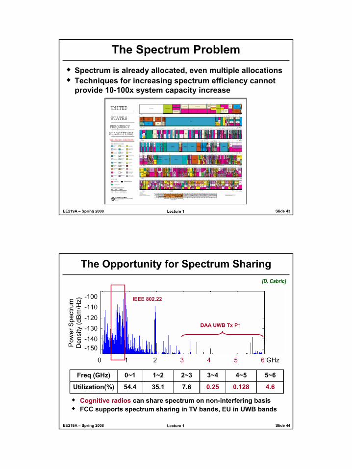
The Spectrum ProblemSpectrum is already allocated, even multiple allocationsTechniques for increasing spectrum efficiency cannot provide 10-100x system capacity increase
Slide 44EE219A – Spring 2008 Lecture 1
0 1 2 3 4 5 6 GHz
7.635.154.4Utilization(%)
2~31~20~1Freq (GHz)
4.60.1280.25
5~64~53~4
Pow
er S
pect
rum
D
ensi
ty (d
Bm/H
z)
-150
-100-110-120-130-140
IEEE 802.22
DAA UWB Tx P↑
The Opportunity for Spectrum Sharing
Cognitive radios can share spectrum on non-interfering basisFCC supports spectrum sharing in TV bands, EU in UWB bands
[D. Cabric]

Slide 45EE219A – Spring 2008 Lecture 1
Sense the spectral environment over a wide bandwidthTransmit in “white space” & Adapt bandwidth and power Detect if primary user appears Move to new white space
PS
D
Frequency
PU1
PU2
PU3
PU4
CR1
CR2
Primary
Cognitive
How Does a Cognitive Radio Operate?[D. Cabric]
Slide 46EE219A – Spring 2008 Lecture 1
MIMO in Neuroscience
[M.A.L. Nicolelis, Actions from thoughts, Nature 409 (2001), pp. 403–407.]

Slide 47EE219A – Spring 2008 Lecture 1
Neural spikesRaw electrical signal
Capturing Electrical Signals in the Brain[T. Meng, Stanford]
Slide 48EE219A – Spring 2008 Lecture 1
Data-collecting mote acquires and filters neural signalsGateway mote receives neural signals and communicates configuration settings with the data-collecting moteRouting PC forwards data over an Ethernet connectionArchive server stores and hosts the neural dataClient application browses data and sets recording parameters
Mote-Based Neural Recording System[S. Farshchi, J. Judy, UCLA]

Slide 49EE219A – Spring 2008 Lecture 1
Typical Spike Waveform
[S. Gibson]
Slide 50EE219A – Spring 2008 Lecture 1
Traces Before Spike Sorting

Slide 51EE219A – Spring 2008 Lecture 1
Spike Sorting in a Nutshell
Sortedspikes
Colored trajectoriesSpiketrajectories
Back annotate
Featu
re x‐
tract
Originalspikes
Clustering
Slide 52EE219A – Spring 2008 Lecture 1
Focus of This Course
3 components of the design problem
Algorithm specification – Matlab (or C)– Floating point, implementation independent, system
simulation
Architecture mapping– Simulink for data flow– Stateflow for control
Hardware optimizations– Real-time emulation– FPGA/ASIC implementation

Slide 53EE219A – Spring 2008 Lecture 1
Major Topic Areas
System modeling– Channels– Interference
Wireless system algorithms– Synchronization– Modulation/Demodulation– Error correction
Neural signal processing– Spike sorting
Computational blocks– FFT– Cordic– Viterbi– …
Architectures– Direct mapped– Time multiplexed– Reconfigurable– Software
programmable