Embed Size (px)
Citation preview
Introduction Chip designers face a bewildering array of choices
– What is the best circuit topology for a function?– How many stages of logic give least delay?– How wide should the transistors be?
Logical effort is a method to make these decisions– Uses a simple model of delay– Allows back-of-the-envelope calculations– Helps make rapid comparisons between alternatives– Emphasizes remarkable symmetries
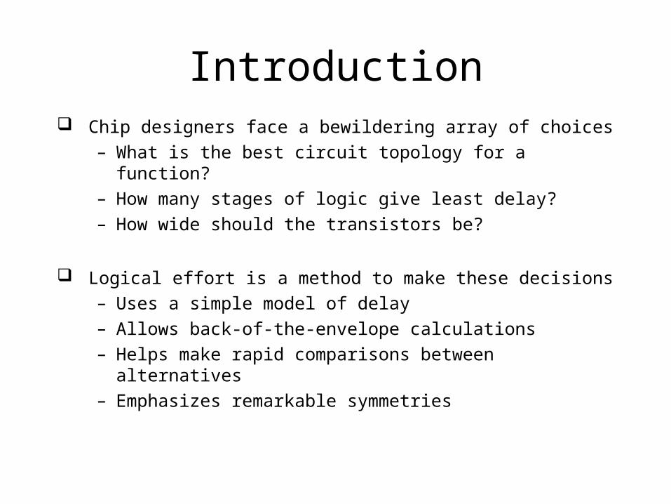
Example Engineer N. T. Bright is the memory designer for an embedded
automotive processor. Help N. T. Bright design the decoder for a register file.
Decoder specifications:– 16 word register file– Each word is 32 bits wide– Each bit presents load of 3 unit-sized transistors– True and complementary address inputs A[3:0]– Each input may drive 10 unit-sized transistors
N. T. needs to decide:– How many stages to use?– How large should each gate be?– How fast can decoder operate?
A[3:0] A[3:0]
16
32 bits
16 words
4:16 Decoder
Register File
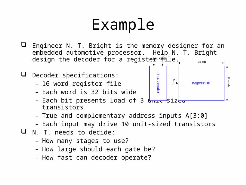
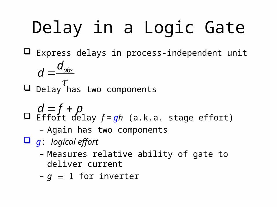
Delay in a Logic Gate Express delays in process-independent unit
absdd
3RC
12 ps in 180 nm process
40 ps in 0.6 m process
Delay in a Logic Gate Express delays in process-independent unit
Delay has two components
Effort delay f = gh (a.k.a. stage effort)– Again has two components
g: logical effort– Measures relative ability of gate to deliver current– g 1 for inverter
absdd
d f p
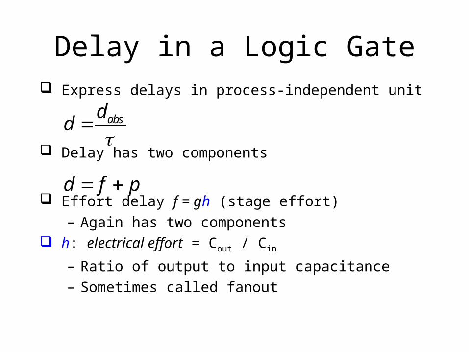
Delay in a Logic Gate Express delays in process-independent unit
Delay has two components
Effort delay f = gh (stage effort)– Again has two components
h: electrical effort = Cout / Cin
– Ratio of output to input capacitance– Sometimes called fanout
absdd
d f p
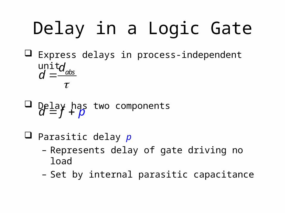
Delay in a Logic Gate Express delays in process-independent unit
Delay has two components
Parasitic delay p– Represents delay of gate driving no load– Set by internal parasitic capacitance
absdd
d pf
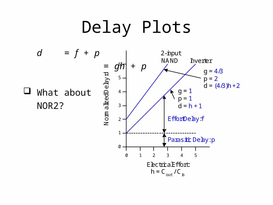
Delay Plotsd = f + p
= gh + p
What about
NOR2?
Electrical Effort:h = C
out / C
in
Nor
mal
ized
Del
ay: d
Inverter2-inputNAND
g = 1p = 1d = h + 1
g = 4/3p = 2d = (4/3)h + 2
Effort Delay: f
Parasitic Delay: p
0 1 2 3 4 5
0
1
2
3
4
5
6
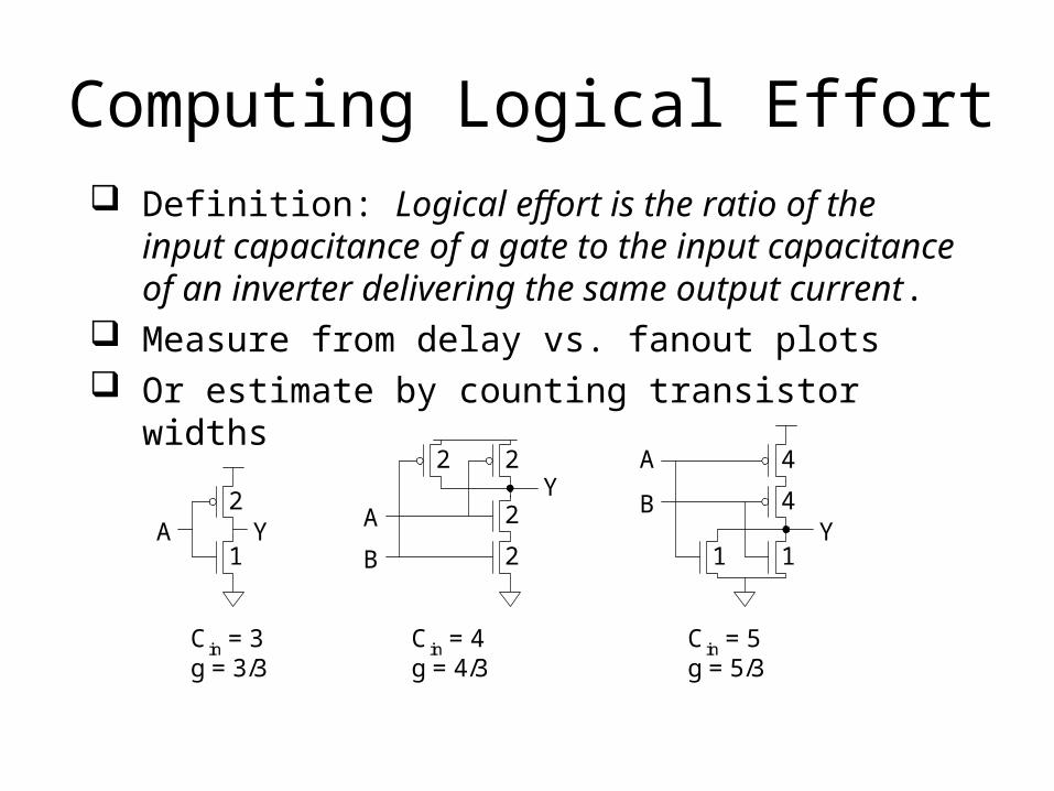
Computing Logical Effort Definition: Logical effort is the ratio of the input
capacitance of a gate to the input capacitance of an inverter delivering the same output current.
Measure from delay vs. fanout plots Or estimate by counting transistor widths
A YA
B
YA
BY
1
2
1 1
2 2
2
2
4
4
Cin = 3g = 3/3
Cin = 4g = 4/3
Cin = 5g = 5/3
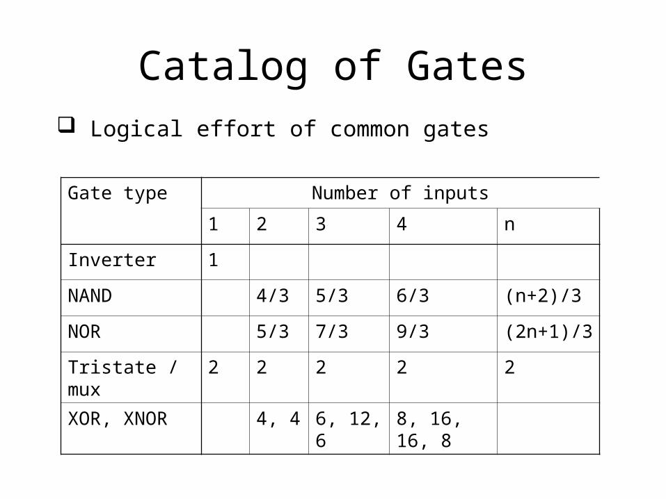
Catalog of Gates
Gate type Number of inputs
1 2 3 4 n
Inverter 1
NAND 4/3 5/3 6/3 (n+2)/3
NOR 5/3 7/3 9/3 (2n+1)/3
Tristate / mux 2 2 2 2 2
XOR, XNOR 4, 4 6, 12, 6 8, 16, 16, 8
Logical effort of common gates
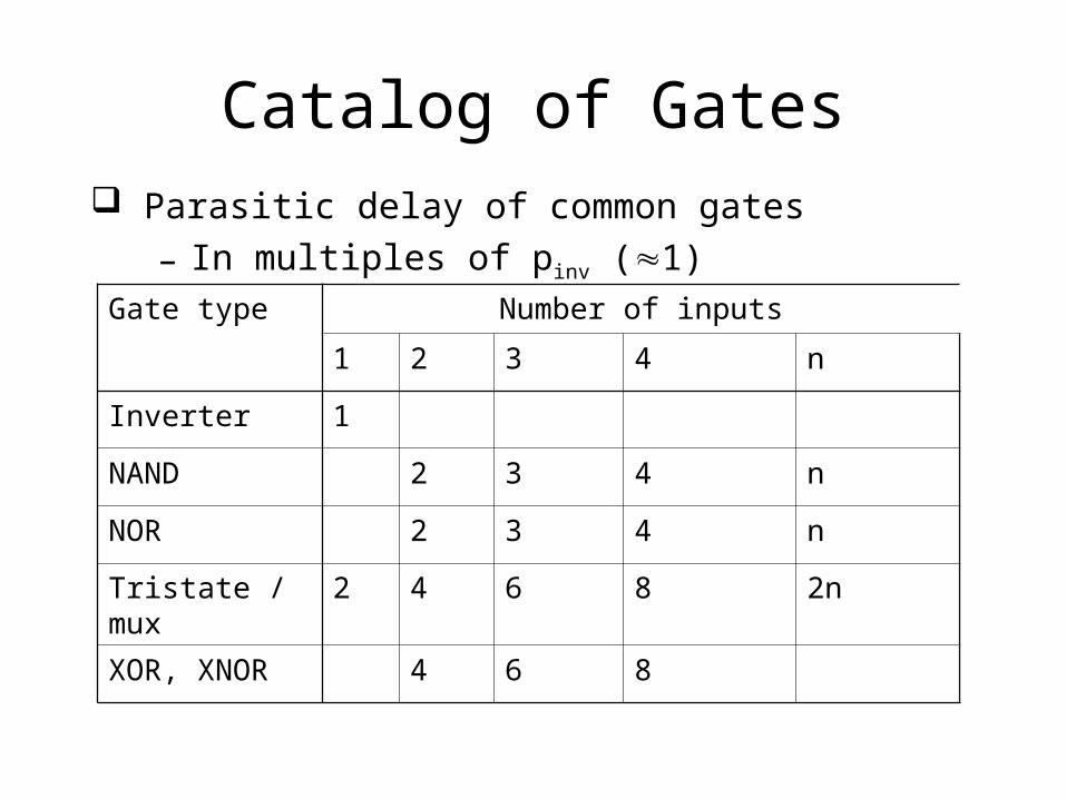
Catalog of Gates
Gate type Number of inputs
1 2 3 4 n
Inverter 1
NAND 2 3 4 n
NOR 2 3 4 n
Tristate / mux 2 4 6 8 2n
XOR, XNOR 4 6 8
Parasitic delay of common gates
– In multiples of pinv (1)
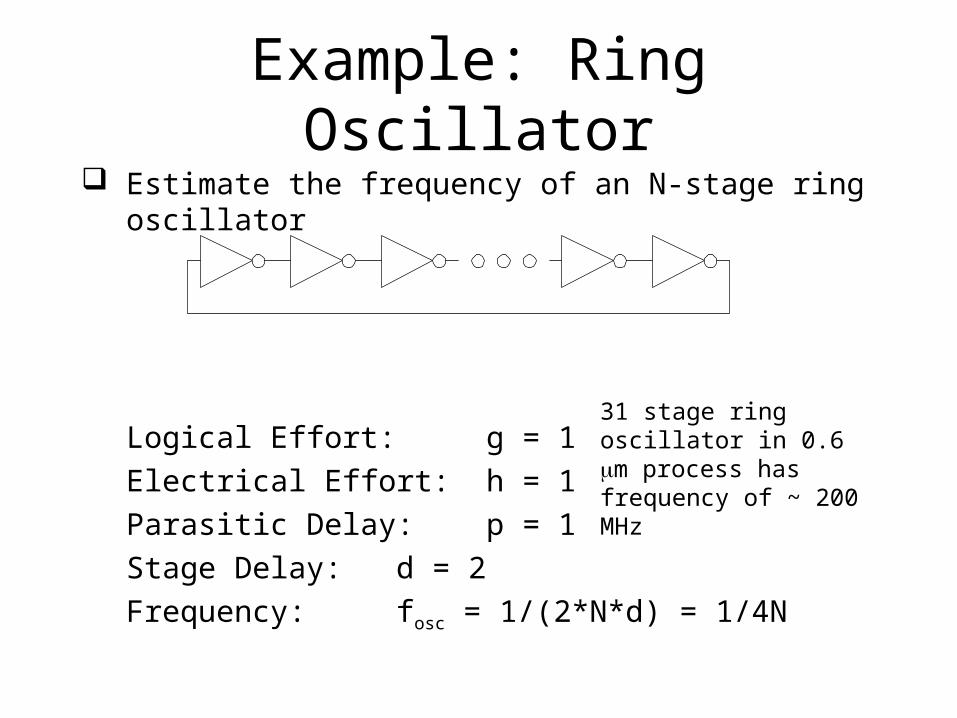
Example: Ring Oscillator Estimate the frequency of an N-stage ring oscillator
Logical Effort: g = 1
Electrical Effort: h = 1
Parasitic Delay: p = 1
Stage Delay: d = 2
Frequency: fosc = 1/(2*N*d) = 1/4N
31 stage ring oscillator in 0.6 m process has frequency of ~ 200 MHz
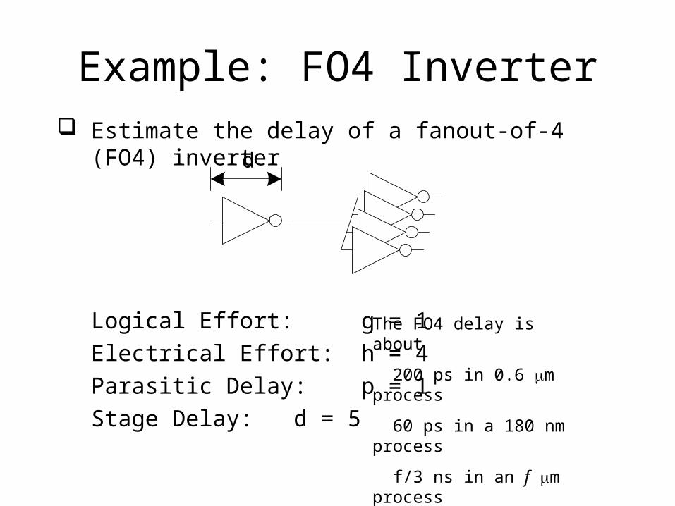
Example: FO4 Inverter Estimate the delay of a fanout-of-4 (FO4) inverter
Logical Effort: g = 1
Electrical Effort: h = 4
Parasitic Delay: p = 1
Stage Delay: d = 5
d
The FO4 delay is about
200 ps in 0.6 m process
60 ps in a 180 nm process
f/3 ns in an f m process
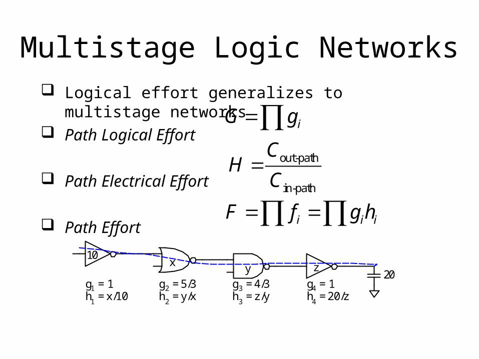
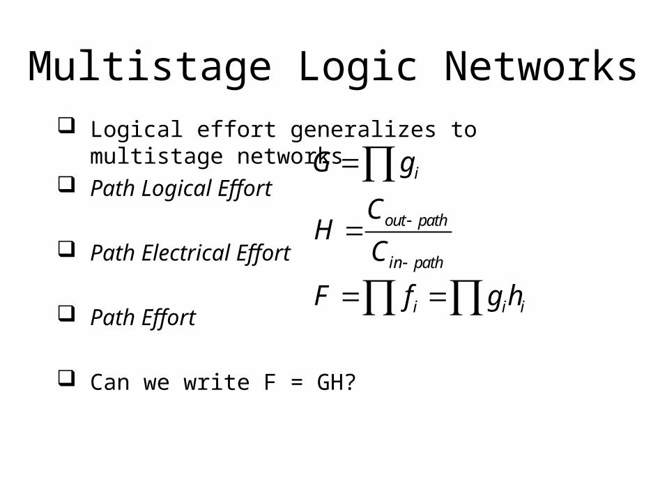
Multistage Logic Networks Logical effort generalizes to multistage networks Path Logical Effort
Path Electrical Effort
Path Effort
iG gout-path
in-path
CH
C
i i iF f g h 10
x y z20
g1 = 1h
1 = x/10
g2 = 5/3h
2 = y/x
g3 = 4/3h
3 = z/y
g4 = 1h
4 = 20/z
Multistage Logic Networks Logical effort generalizes to multistage networks Path Logical Effort
Path Electrical Effort
Path Effort
Can we write F = GH?
iG gout path
in path
CH
C
i i iF f g h
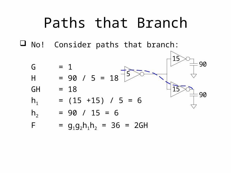
Paths that Branch No! Consider paths that branch:
G = 1
H = 90 / 5 = 18
GH = 18
h1 = (15 +15) / 5 = 6
h2 = 90 / 15 = 6
F = g1g2h1h2 = 36 = 2GH
5
15
1590
90
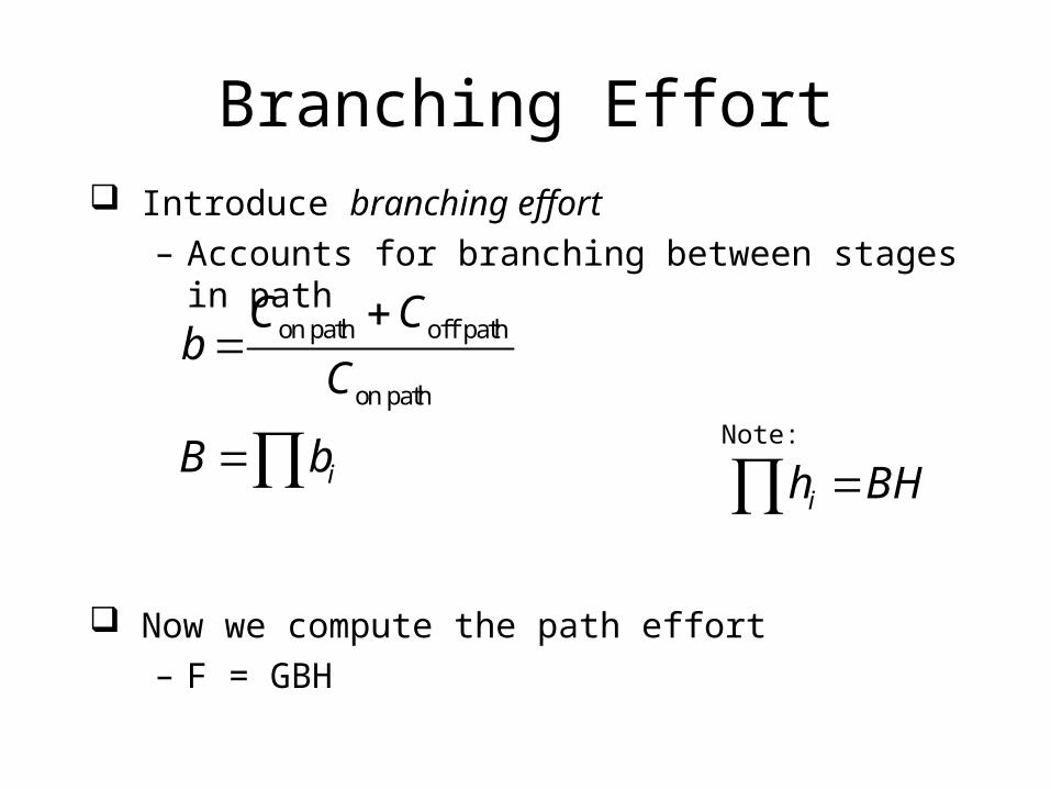
Branching Effort Introduce branching effort
– Accounts for branching between stages in path
Now we compute the path effort– F = GBH
on path off path
on path
C Cb
C
iB bih BH
Note:
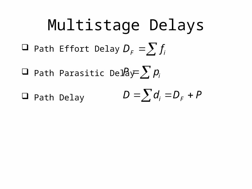
Multistage Delays Path Effort Delay
Path Parasitic Delay
Path Delay
F iD fiP pi FD d D P
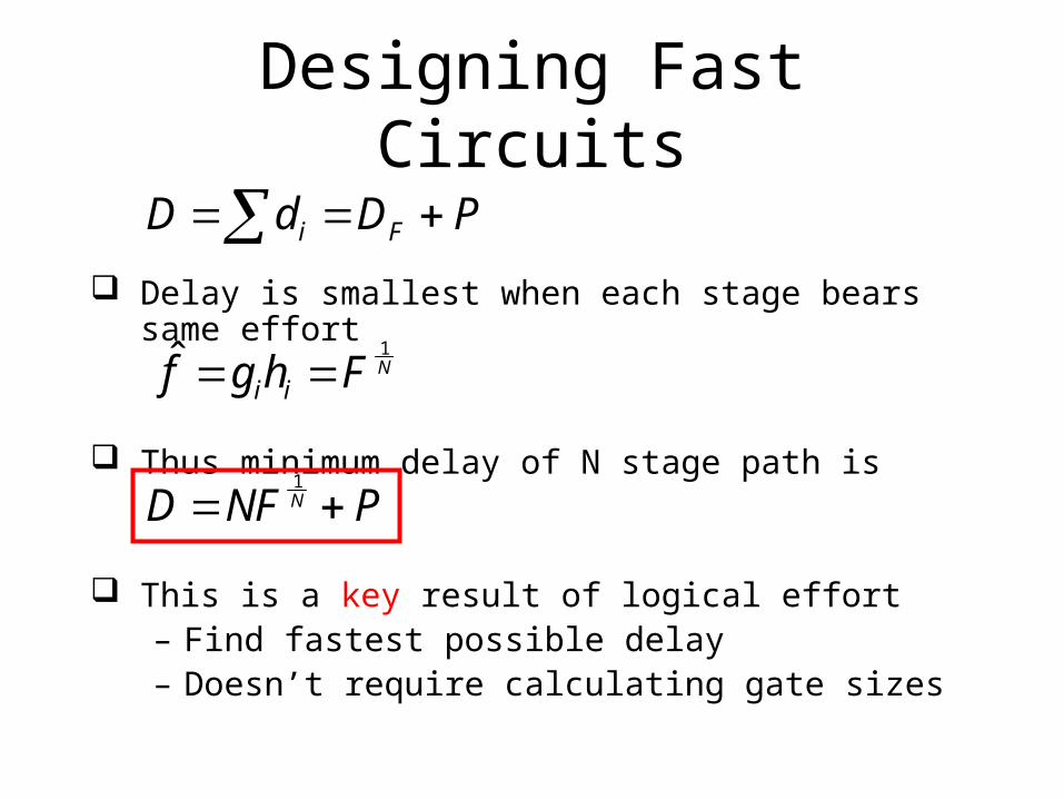
Designing Fast Circuits
Delay is smallest when each stage bears same effort
Thus minimum delay of N stage path is
This is a key result of logical effort– Find fastest possible delay– Doesn’t require calculating gate sizes
i FD d D P
1ˆ Ni if g h F
1ND NF P
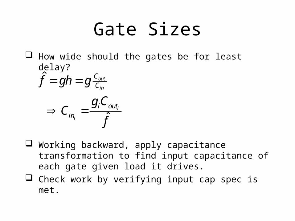
Gate Sizes How wide should the gates be for least delay?
Working backward, apply capacitance transformation to find input capacitance of each gate given load it drives.
Check work by verifying input cap spec is met.
ˆ
ˆ
out
in
i
i
CC
i outin
f gh g
g CC
f
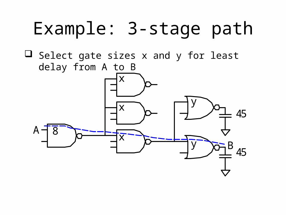
Example: 3-stage path Select gate sizes x and y for least delay from A to B
8 x
x
x
y
y
45
45
A
B
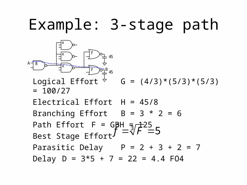
Example: 3-stage path
Logical Effort G = (4/3)*(5/3)*(5/3) = 100/27
Electrical Effort H = 45/8
Branching Effort B = 3 * 2 = 6
Path Effort F = GBH = 125
Best Stage Effort
Parasitic Delay P = 2 + 3 + 2 = 7
Delay D = 3*5 + 7 = 22 = 4.4 FO4
8 x
x
x
y
y
45
45
A
B
3ˆ 5f F
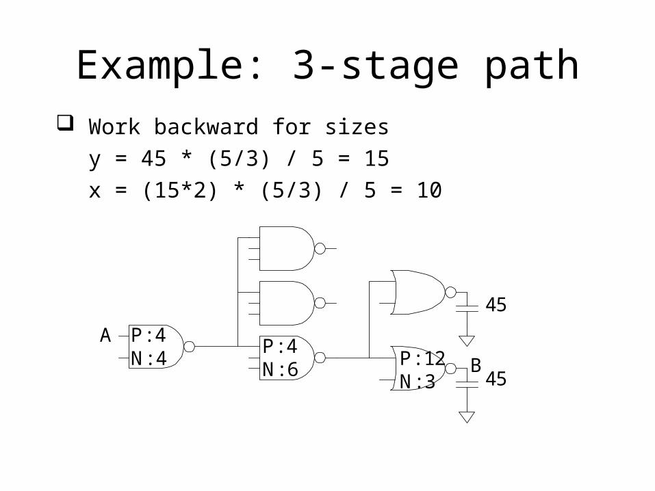
Example: 3-stage path Work backward for sizes
y = 45 * (5/3) / 5 = 15
x = (15*2) * (5/3) / 5 = 10
P: 4N: 4
45
45
A
BP: 4N: 6
P: 12N: 3
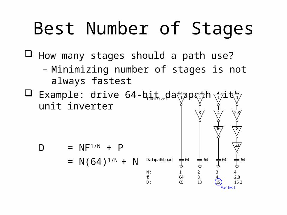
Best Number of Stages How many stages should a path use?
– Minimizing number of stages is not always fastest Example: drive 64-bit datapath with unit inverter
D = NF1/N + P
= N(64)1/N + N
1 1 1 1
8 4
16 8
2.8
23
64 64 64 64
Initial Driver
Datapath Load
N:f:D:
16465
2818
3415
42.815.3
Fastest
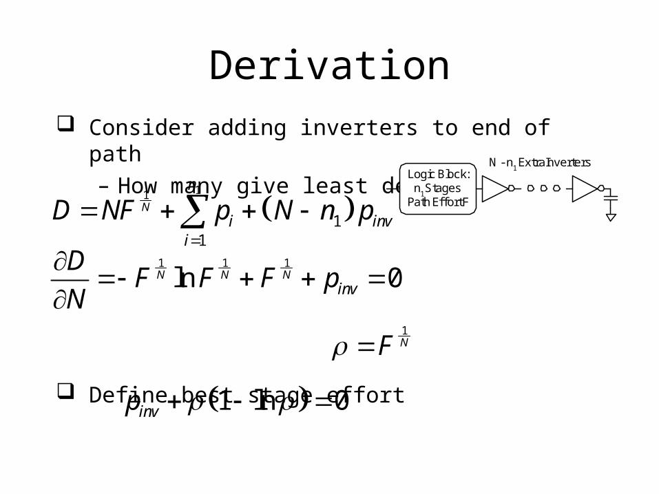
Derivation Consider adding inverters to end of path
– How many give least delay?
Define best stage effort
N - n1 Extra Inverters
Logic Block:n
1 Stages
Path Effort F 11
11
N
n
i invi
D NF p N n p
1 1 1
ln 0N N Ninv
DF F F p
N
1 ln 0invp
1NF
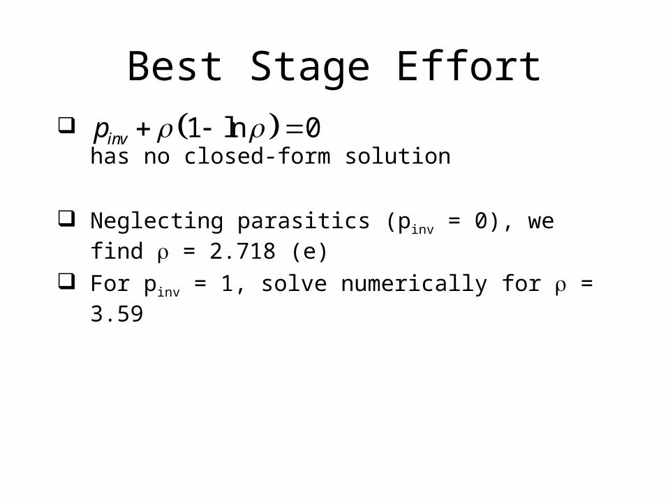
Best Stage Effort has no closed-form solution
Neglecting parasitics (pinv = 0), we find = 2.718 (e)
For pinv = 1, solve numerically for = 3.59
1 ln 0invp
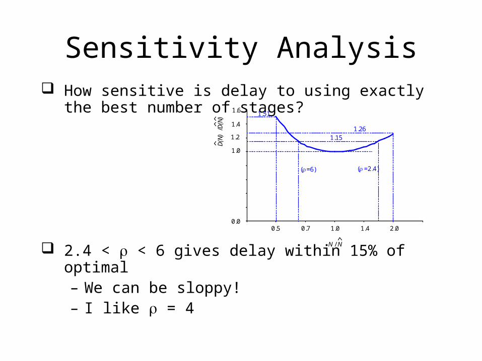
Sensitivity Analysis How sensitive is delay to using exactly the best
number of stages?
2.4 < < 6 gives delay within 15% of optimal– We can be sloppy!– I like = 4
1.0
1.2
1.4
1.6
1.0 2.00.5 1.40.7
N / N
1.151.26
1.51
( =2.4)(=6)
D(N
) /D
(N)
0.0
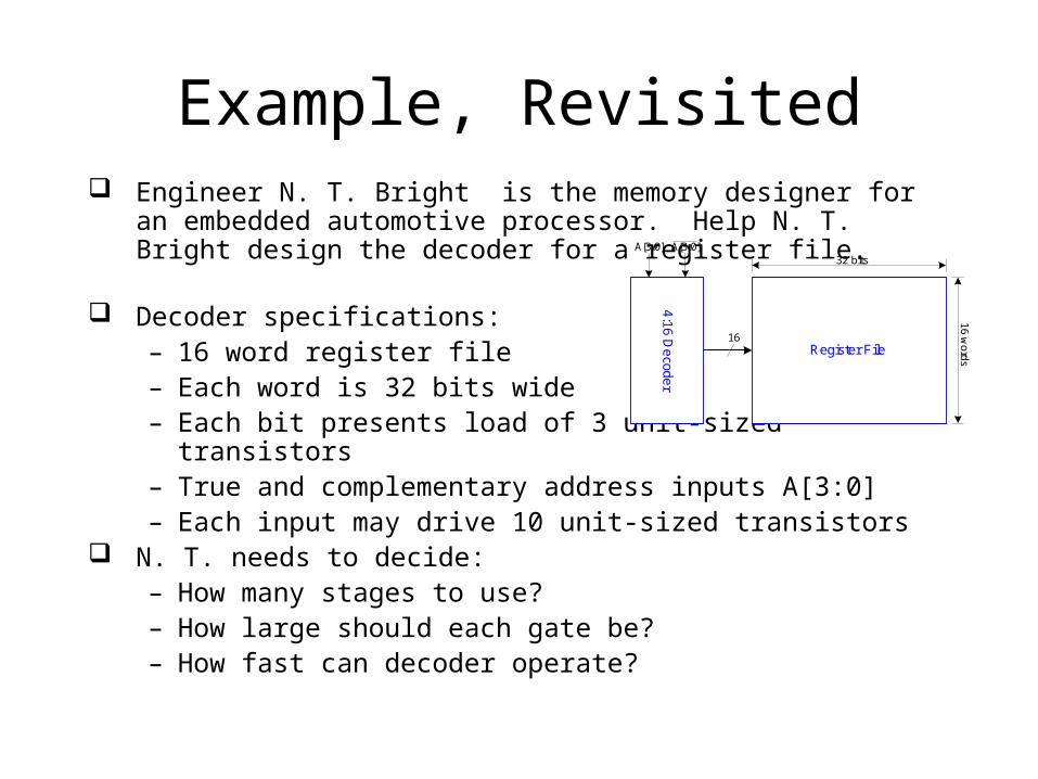
Example, Revisited Engineer N. T. Bright is the memory designer for an
embedded automotive processor. Help N. T. Bright design the decoder for a register file.
Decoder specifications:– 16 word register file– Each word is 32 bits wide– Each bit presents load of 3 unit-sized transistors– True and complementary address inputs A[3:0]– Each input may drive 10 unit-sized transistors
N. T. needs to decide:– How many stages to use?– How large should each gate be?– How fast can decoder operate?
A[3:0] A[3:0]
16
32 bits
16 words
4:16 Decoder
Register File
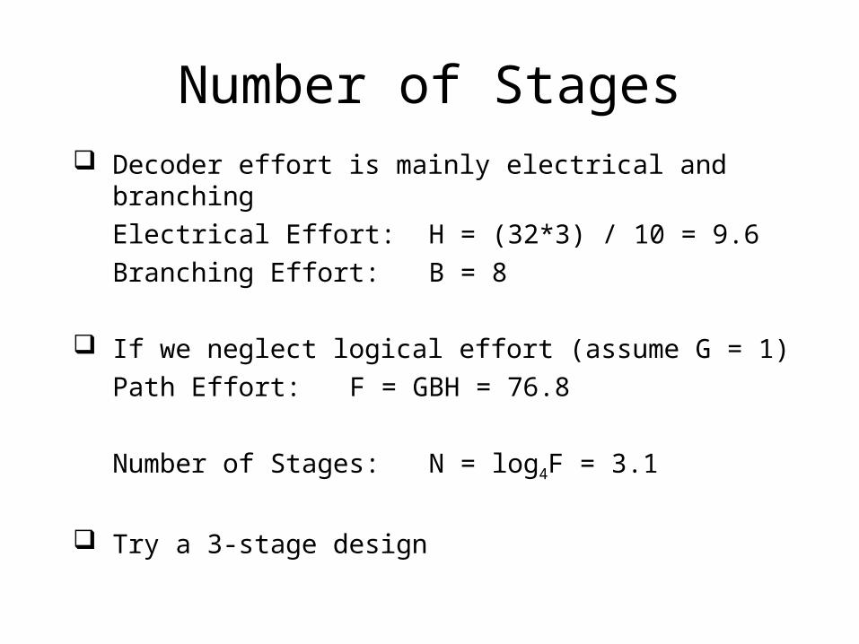
Number of Stages Decoder effort is mainly electrical and branching
Electrical Effort: H = (32*3) / 10 = 9.6
Branching Effort: B = 8
If we neglect logical effort (assume G = 1)
Path Effort: F = GBH = 76.8
Number of Stages: N = log4F = 3.1
Try a 3-stage design
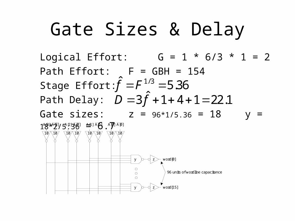
Gate Sizes & DelayLogical Effort: G = 1 * 6/3 * 1 = 2
Path Effort: F = GBH = 154
Stage Effort:
Path Delay:
Gate sizes: z = 96*1/5.36 = 18 y = 18*2/5.36 = 6.7A[3] A[3] A[2] A[2] A[1] A[1] A[0] A[0]
word[0]
word[15]
96 units of wordline capacitance
10 10 10 10 10 10 10 10
y z
y z
1/3ˆ 5.36f F ˆ3 1 4 1 22.1D f
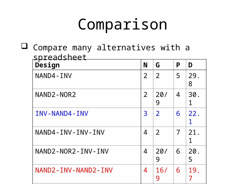
Comparison Compare many alternatives with a spreadsheet
Design N G P D
NAND4-INV 2 2 5 29.8
NAND2-NOR2 2 20/9 4 30.1
INV-NAND4-INV 3 2 6 22.1
NAND4-INV-INV-INV 4 2 7 21.1
NAND2-NOR2-INV-INV 4 20/9 6 20.5
NAND2-INV-NAND2-INV 4 16/9 6 19.7
INV-NAND2-INV-NAND2-INV 5 16/9 7 20.4
NAND2-INV-NAND2-INV-INV-INV 6 16/9 8 21.6
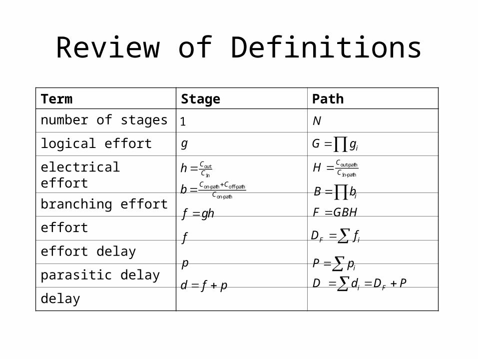
Review of Definitions
Term Stage Path
number of stages
logical effort
electrical effort
branching effort
effort
effort delay
parasitic delay
delay
iG gout-path
in-path
C
CH
N
iB bF GBH
F iD f
iP pi FD d D P
out
in
CCh
on-path off-path
on-path
C C
Cb
f gh
f
p
d f p
g
1
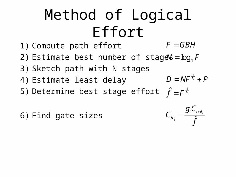
Method of Logical Effort1) Compute path effort
2) Estimate best number of stages
3) Sketch path with N stages
4) Estimate least delay
5) Determine best stage effort
6) Find gate sizes
F GBH
4logN F
1ND NF P
1ˆ Nf F
ˆi
i
i outin
g CC
f
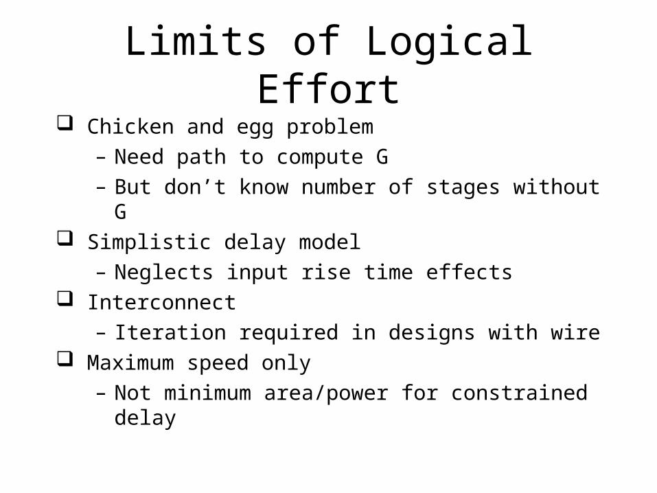
Limits of Logical Effort Chicken and egg problem
– Need path to compute G– But don’t know number of stages without G
Simplistic delay model– Neglects input rise time effects
Interconnect– Iteration required in designs with wire
Maximum speed only– Not minimum area/power for constrained delay
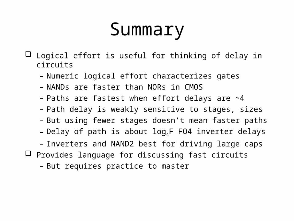
Summary Logical effort is useful for thinking of delay in circuits
– Numeric logical effort characterizes gates– NANDs are faster than NORs in CMOS– Paths are fastest when effort delays are ~4– Path delay is weakly sensitive to stages, sizes– But using fewer stages doesn’t mean faster paths
– Delay of path is about log4F FO4 inverter delays
– Inverters and NAND2 best for driving large caps Provides language for discussing fast circuits
– But requires practice to master