Embed Size (px)
Citation preview
Introducing the Xilinx Spartan Series
High Performance, Low Cost FPGAs with on-chip Select-RAM

Xilinx Spartan Families Complete High Volume FPGA Solution
Spartan: 5 Volt with up to 40K System Gates SpartanXL: 3.3 Volt with up to 40K System Gates Xilinx Alliance and Foundation Software
Process technology leap UltraDenseTM 0.5m for 5 Volt Spartan Family UltraDenseTM 0.35m for 3.3 Volt SpartanXL Family
XC4000 heritage Powerful software tools Most successful FPGA architecture
No compromises Performance, RAM, Cores, and Low Price

Basic Architecture
Array of CLBs surrounded by perimeter IOBs
Special functions in corners

Spartan Meets ASIC RequirementsLow Price
Unit Cost
Development Cost
Unit Cost
Development Cost
NRE
LostOpportunity
Cost of Ownership
Per Unit ($)
FPGAASIC
FPGA Cost of Ownership Advantage No test vectors required Limited or no simulation Automatic Place and Route Re-spins in hours not months Faster Time-to-Market No NRE
1x
2x
10x

Total Cost Management
Leading edge process technology Smallest die size
Streamlined feature set Synchronous single/dual-port Select-RAM Popular serial configuration modes JTAG support
Optimized manufacturing test flow for low cost
Focused package offering Highest volume plastic PLCC, VQ, TQ, PQ, BGA packages

0
1
2
3
4
0.6u FPGA2LM
0.6u FPGA3LM
0.5u FPGA3LM
Ultradense0.5u FPGA
AssemblyTestSilicon
Total Cost Management
Relative Cost
1993
1995
1996
Spartan Series addresses all aspects of cost
1997
Majority of cost is back end (assembly, test, overhead)
Spartan die are pad limited

Packages Focus on popular, low-cost packages
Highest-volume ASIC plastic packages
Only six packages: PC84 (05/10) VQ100 (05/10/20/30) TQ144 (10/20/30) PQ208 (20/30/40) PQ240 (30/40) BG256 (30/40)
Optimized PQ208 pinout Adds more I/O

UltraDenseTM 0.5 Process
ChipTransistor gates 0.5- allows 3.3 V supply
All other features 0.35- small size- low capacitance- performance- low power
Combines 5 V operation with 0.35 benefits

UltraDenseTM Process
Core
core-limited
I/O padsGate count determines
die size
Spartan Die Size for High I/O packageNearly Equivalent to Gate Arrays
pad-limited
Core
I/O pads
I/O countdetermines
die size

Advanced Process Technology eliminates the “RAM compromise”
Die Sizewithout RAM
1.0
Logicand RAM
I/O pads Die Sizewith RAM
1.0
Logic
Empty, wasted die
area
Technology advances have reduced die size faster than pad technology

Xilinx Spartan Series
5 Volt -> XCS05 XCS10 XCS20 XCS30 XCS40
3.3 Volt -> XCS05XL XCS10XL XCS20XL XCS30XL XCS40XL
System Gates 2K-5K 3K-10K 7K-20K 10K-30K 13K-40K
Logic Cells 238 466 950 1368 1862
Max Logic Gates 3,000 5,000 10,000 13,000 20,000
Flip-Flops 360 616 1120 1536 2016
Max RAM bits 3,200 6,272 12,800 18,432 25,088
Max I/O 80 112 160 192 224
Performance 80MHz 80MHz 80MHz 80MHz 80MHz
No Compromises: Performance, RAM, Cores, and Low Price

Spartan Series Footprint Compatibility
5 Volt XCS05 XCS10 XCS20 XCS30 XCS40
3.3 Volt XCS05XL XCS10XL XCS20XL XCS30XL XCS40XL
PC84 PC84
VQ100 VQ100 VQ100 VQ100
TQ144 TQ144 TQ144
PQ208 PQ208 PQ208
PQ240 PQ240
BG256 BG256
Highest volume ASIC plastic packages
Footprint compatible in common packages

Xilinx Introduces First Fully Programmable
System Solution
First FPGA Architecture Designed for Intellectual Property

System Level Design Trend
DSP
CustomLogic
BusI/F
RAMI/F
High-DensityHigh-PerformanceCustom Device
PCI
Scratch PadSRAM
PC Board

High SpeedSynchronous
DRAM(Mbytes)
VideoData In
Frame DataBlock
SelectRAMMemory(Kbytes)
BlockSelectRAM
Memory(kbytes)
DistributedSelectRAM
Memory(bytes)
Line Data
DistributedSelectRAM
Memory(bytes)
Pixel Data
Video PixelProcessing
Function(logic)
ProcessedVideo Out
Real Time Video Processor
Virtex FPGA
Hierarchy of RAM provides efficient and very high bandwidth data processing

Virtex Family Overview
0.25um, 5 layer metal processDensity: 50 thousand to 1 million system gates
Performance 100+ MHz performance (3-4 levels) 160 MHz system performance
First device in 2Q98 250,000 system gates One million system gate device by end of 1998

Functional Block Diagram
CLB Segmented routing
SelectI/OPins
DistributedSelectRAMMemory
BlockSelectRAMMemory
PLL
66 MHz PCI SSTL3
Vector BasedInterconnectdelay=f(vector)

2 LCs 2 LCs
CLB
4 InputLUT
RegisterCarryand
Control
I3I2I1I0
O
WI DI
DCE
CLK
Q
CO
CI
4 InputLUT
RegisterCarryand
Control
I3I2I1I0
O
WI DI
DCE
CLK
Q
CO
CI
PR
RS
PR
RS
Polarity of all control signals selectable
Fast arithmetic and multiplier circuitry
Optimized for synthesis
Virtex Configurable Logic Block

Segmented Routing Interconnect
3-STATE BUSSES
SWITCH
MATRIX
2 LCs 2 LCs
CA
RR
Y
CA
RR
Y
CLB
CA
RR
Y
CA
RR
Y
Fast local routing within CLBs
General purpose routing between CLBs
Fast Interconnect 8ns across 250,000
system gates
Predictable for early design analysis
Optimized for five layer metal process

Block RAM
Configure as: 4096 bits with variable aspect ratio
8-32 blocks per device
True dual-port, fully synchronous operation Cycle time <10 ns
Flexible block RAM configuration 5 blocks: 2K x 10 video line buffer 1 block: 512 x 8 ATM buffer (9 frames) 4 blocks: 2K x 8 FIFO 9 blocks: 4K x 9 FIFO with parity
WEAENACLKAADDRADINA
DOA
DOB
RAMB4
WEBENBCLKBADDRBDINB

Virtex FPGA Performance 100+ MHz internal speeds
155 MHz SONET data stream processing 100+ MHz Pipelined Multipliers 66 MHz PCI
100+ MHz system interface speeds
without PLL with PLL
Tco (output register) 6 ns 3.5 nsTsu (input register) 3 ns 3 nsTh (input register) 0 ns 0 nsMax I/O performance 110 MHz 160 MHz
Virtex FPGAs Deliver World-Class Performance!

Today’s Gate Array
Gate Array
XC5200 Series

XC5200 Family Overview
Flexible FPGA Product Family: - 5 Devices Ranging from 3,000 - 23,000 usable gates- 5-Volt and 3-Volt Devices
Low cost, process-optimized architecture Xilinx FPGA Innovations:
- VersaBlockTM
Logic Module- VersaRing
TM I/O Interface
6 Levels of Interconnect Hierarchy Performance Up to 50MHz Robust Feature Set:
- Carry Logic - 3-state buffers- Cascade Chain - 4 Global Nets- JTAG Logic - Slew rate control

Flexible XC5200 Feature SetXC5200 Feature BenefitArchitecture-optimized 0.6u process Smallest die size - lowest cost
VersaBlockTM
logic module Versatile logic PLUS abundant local routing
VersaRingTM
I/O interface High logic utilization AND increased pin
assignment flexibility
Simple logic cell resources Efficient synthesis results
Carry logic Fast arithmetic functions
Cascade chain Efficient wide-input functions
Logic cell feed through Logic cell = logic and routing at the same time
Independent logic cell I/Os Easy access to logic resources
Boundary Scan logic Enhanced board / system testability
3-state buffers On-chip bussing
4 global buffers Fast, low skew signal distribution
Slew rate control High performance and reduced noise

XC5200 Architecture Overview
XC5200 first FPGA to combine: 0.6um CMOS SRAM process Triple-layer metal (TLM) New, process-optimized
architecture
Result: FPGA Efficiency Breakthrough
Most gates / mm2 More routing for less cost
Architecture Highlights: VersaBlockTM logic module VersaRingTM I/O interface General Routing Matrix (GRM)
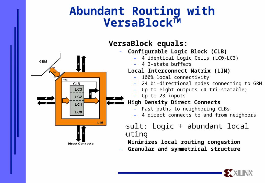
Abundant Routing with VersaBlockTM
VersaBlock equals:— Configurable Logic Block (CLB)
– 4 identical Logic Cells (LC0-LC3)– 4 3-state buffers
— Local Interconnect Matrix (LIM)– 100% local connectivity– 24 bi-directional nodes connecting to GRM– Up to eight outputs (4 tri-statable)– Up to 23 inputs
— High Density Direct Connects– Fast paths to neighboring CLBs– 4 direct connects to and from neighbors
Result: Logic + abundant local routing— Minimizes local routing congestion— Granular and symmetrical structure

XC5200 Configurable Logic Block
Configurable Logic Block (CLB) 4 Identical Logic Cells 20 independent inputs 12 independent outputs 2 independent 5-input functions
Logic Cell (LC0 - LC3) Function generator, register, & control logic Independently usable F & FD Programmable flip flop or latch option Fast carry logic Cascade chain Independent feed-through capability

Abundant Routing Resources
6 Levels of Hierarchy
General Routing Matrix:
1. 10 single length lines
2. 4 double length lines
3. 8 longlines per row and channel
VersaBlock:
4. Local Interconnect Matrix (LIM)
5. Direct connects to all neighbors:
- 4 uni-directional lines in
- 4 uni-directional lines out
6. Logic cell feedthrough
SingleLengthLines
DoubleLengthLines
DirectConnects
Longlines
LocalInterconnect
Matrix

VersaRingTM: High Utilization & Pin Assignment Flexibility
Versatile interface between internal logic and I/O:
— I/O decoupled from core logic— Incremental edge routing resources
VersaRing resources include:— 8 horizontal longlines— 8 vertical longlines— 4 direct connects in per side— 4 direct connects out per side— 4 double length lines to GRM— 10 single length lines to GRM— 8 single length lines to adjacent VersaRing tile

XC5200 Family
XC5202 XC5204 XC5206 XC5210 XC5215Max Logic Gates 3,000 6,000 10,000 16,000 23,000Typical Gate Range 2-3K 4-6K 6-10K 10-16K 15-23KLogic Cells 256 480 784 1,296 1,936Flip-Flops 256 480 784 1,296 1,936Max I/O 84 124 148 196 244Performance -6/-5/-4/-3 -6/-5/-4/-3 -6/-5/-4/-3 -6/-5/-4/-3 -6/-5/-4/-3Packages: PC84 PC84 PC84 PC84
PQ100 PQ100 PQ100 VQ100 VQ100 VQ100 TQ144 TQ144 TQ144 TQ144
PQ160 PQ160 PQ160 PQ160 TQ176 TQ176PQ208 PQ208 HQ208
BG225 BG225PQ240 HQ240
HQ304 BG352
PG156 PG156 PG191 PG223 PG299
100% 100% Footprint Footprint Compatibility in Compatibility in
Common PackagesCommon Packages


What is the CPLD
• Similar to having multiple PAL devices interconnected in one chip
• Best applications Wide functions Fast arithmetic Complex counters Complex state machines PAL/GAL or TTL integration Non-volatile
PAL
PAL
PAL
PAL
Swi-tch
Mat-rix
Prog.ANDarray
FixedOR
array
FF/Macro-
cell
FF/Macro-
cell

Functions of 5 Product Term are fastest
Xilinx CPLDs use a Sum of Products Architecture
From 5 P-terms to 15 P-terms cost under 1ns of tpd
AND functions are “free”, Ors are not. An OR gate equals a Macrocell
Inverters are free
36 Input 5 Product Term

Pin Selection For CPLD
Remember the JTAG programming pins
Join the CPLDs in the same JTAG Daisy Chain for board debug
The Xilinx CPLD JTAG cable has 4mA drive, be sure to buffer the JTAG Signals if more than 5 devices in chain

Why not EEPROM Technology?
3XRouting
Switches
Product benefits due to 67% smaller FLASH cell More routing switches in the same area supports pinlocking Lower parasitic capacitance improves performance Long term cost improvements due to scalability
Greatly improved endurance with FLASH Lower program/erase voltages
Source
Data
Word Line
Control
Ground
Data
Word Line
Control
Write
Floating Gate
Typical E2 CPLD Cell FastFLASH Cell
Control
Write
Data
Ground
Word Line
Source
Data
Word LineControl
S1
S2
S3
Source
Data
Word Line
Control
Source
Data
Word Line
Control
S1

ISP Market Growth
1997
Non-ISP70%
ISP30%
2000
Non-ISP40%
ISP60%

XC9500 CPLDs
“The New Standard in ISP”

XC9500 Key Features
5 Volt In-System Programmable (ISP) CPLDs
Most complete IEEE 1149.1 JTAG for ISP and Test
High performance: 5ns pin-to-pin
High density: up to 6,400 usable gates
Highest reprogramming reliability 10,000 program/erase cycles 20-year data retention
Industry’s best pin-locking architecture

XC9500 Architecture
FunctionBlock 1
JTAGController
FunctionBlock 2
I/O
FunctionBlock n
3
I/O - Global Tri-States
2 or 4
FunctionBlock 3
I/O
In-SystemProgramming Controller
FastCONNECTSwitch Matrix
JTAG Port
3
I/O
I/O
I/O - Global Set/Reset
I/O - Global Clocks
I/OBlocks
1

FunctionBlock
FastCONNECT
Complete Interconnectivitywith FastCONNECT™
JTAG
GlobalS/R
GlobalClocks
FunctionBlock
FunctionBlock
FunctionBlock
FunctionBlock
FunctionBlock
FunctionBlock
FunctionBlock
Global3-State

XC9500 FastCONNECT
Pin Inputs(~ 3 entries / FB)
Macrocells(36 entries / FB)
1
2
3
4
36

FastFLASH Function Block
ToFastCONNECT
FromFastCONNECT
23 Global3-State
GlobalClocks
I/O
I/O
36
Product-Term
Allocator
Macrocell 1
ANDArray
Macrocell 18

XC9500 Macrocell
FromFastCONNECT
36
SUM-TermLogic
D/T Q
R S
to/from other macrocells
RegisterXOR 18
GlobalClocks
GlobalOEs
P-term ClkP-term R&SP-term OE
3 2 or 4
to/from other macrocells
GlobalR/S
P-TermAllocator

Feedback Paths
FastCONNECT
Pin
LocalMacrocell
FastCONNECT
FB X
Macrocell
Macrocell
Pin feedback
FastCONNECT feedback
Local feedback

What is Pin-Locking?
Ability to retain device pin assignments for small to medium design changes
introducing a new variable to existing terms adding input signals inverting signals introducing 1or 2 buried flip flops adding p-terms
Requires a symmetric, uniform architecture
Requires software focus on pin-locking

3 Keys to Pin-Locking
FunctionBlock
FastCONNECT
JTAG
Global3-State
GlobalS/R
GlobalClocks
FunctionBlock
FunctionBlock
FunctionBlock
FunctionBlock
FunctionBlock
FunctionBlock
2nd generation switch matrix:
Complete interconnect of all pins & blocks
All pin-to-pin paths at full speed
FunctionBlock
Fully PopulatedSwitch Matrix

Keys to Pin-Locking
ToFastCONNECT
23 Global3-State
GlobalClocks
I/O
I/O
FromFastCONNECT
36
Macrocell 1
ANDArray
Macrocell 18
ProductTermAllocator
•
Wide FunctionBlock Fan-in
Flexible MacrocellLogic Allocation

XC9500 Supports Design Changeswith Fixed Pinouts
Design Change XC9500 Feature
Add another input FastCONNECT switch matrixpin or FB output with 100% connectivity
Add more logic in XC9500 allows expansionthe macrocell up to 90 P-terms
Add additional input 36 total inputs are available connections to the FB plus FastCONNECT
AND gate capability

CPLD Architecture Designed for Superior Pin-Locking
Routability Excellent Good* Poor Good
Notes: * Decreases with density
Xilinx
XC9500
Altera
Max7KS
Lattice
1K/2K/3K
AMD
Mach5
36
Yes
90
Yes
32
No No
No
36
No
18/24
No No
32 32
32
Fully populated switch
Maximum pterms/Mcell
Bi-directional individual
product term allocation
Function block fan-in

Requirements to Supportthe Product Life Cycle
Prototyping SystemIntegration
FieldUpgrades
ManufacturingPre-production
ManufacturingHigh Volume
In-System Program Pin Locking JTAG High Endurance
High program/erase reliability Thousands of program erase cycles required
Pin Locking Capability Pinout remains the same after design changes
Industry standard JTAG Device programming, logic debugging, manufacturing
board test

XC9500 Other System Features
Enhanced Data Security Features Read security bits prevent unauthorized reading Write security bits prevent accidental program/erase
Reduced power option per macrocell
3.3v/5v outputs
24 mA, 100% PCI compliant
Output Noise Reduction Slew rate control User programmable ground pin capability
User Programmable Ground Pin
User I/O Pin
Ground Pin
User I/O Pin
Internal Logic
Additional Ground Pin• Lower ground inductance• Reduce ground noise

XC9500 Product Family
9536
Macrocells
UsableGates
tPD (ns)
Registers
Max. UserI/Os
36 72 108 144 216
800 1600 2400 3200 4800
5 7.5 7.5 7.5 10
36 72 108 144 216
34 72 108 133 166
Packages 44VQ44PC 44PC
84PC100TQ100PQ
84PC100TQ100PQ160PQ
100TQ100PQ160PQ
288
6400
15
288
192
208HQ352BG
160PQ208HQ352BG
9572
95108
95144 95216 95288

FLASH Process Technology Roadmap
1994 1996 1998 2000
.6
.4
.2
5v
2002
.8
5v
3.3v2.5v
1.8v
5v
Year
Featu
re S
ize (
µ)
1995 1997 1999 2001

Address Decoder Benchmark
Tests effects of routing and function block fan-in on pin locking
a[N:0] out1
b[N:0] out2
FB1
FB2

Address Decoder Design Iteration
a[N:0] out1
b[N:0] out2
FB1
FB2
MODULE swapTITLE 'Bus Swap'
equations
out1 = b_bus == 24;out2 = a_bus == 24;
END
Wrong address bits decoded, address bus rerouted

Address Decoder Pinlock Performance
Altera
Xilinx
Initial Compile
Pinlocked with Changes
All XC9500 -10
16-Bit Bus
10
XC9572 -10and larger
32-Bit Bus
10
XC95108-10and larger
36-Bit Bus
10tPD
(nS)
16-Bit Bus
10
EPM7128S-10and larger
32-Bit Bus
10
EPM7128S-10and larger
36-Bit Bus
10
EPM7128S-10and larger
tPD
(nS)
16-Bit Bus
10
32-Bit Bus
10
ispLSI1048-80
36-Bit Bus
10
20 20
30
20
30
16.419.2 19.2
15
23.319.2
23.3
31.6
23.3
4039.9
12 12
a b c d
ispLSI1016-110ispLSI1024-90ispLSI1032-90ispLSI1048-80
abcd
a b
ispLSI1032-90ispLSI1048-80
ab
tPD
(nS)
Lattice

Address Counter Benchmark
Tests effects of routing and function block fan-in on pinlocking when macrocell feedback is required
adata[N:0] qa[N:0]
bdata[N:0] qb[N:0]
bload
aload
clockhold
ACNT
BCNT

Address Counter Design Iteration
adata[N:0]
bdata[N:0]
qa[N:0]
qb[N:0]
clockhold
bload
aload
ACNT
BCNT
MODULE cntswapequationsacount := bdata & aload # acount & !aload & hold # (acount + 1) & !aload & !hold;acount.clk = clock;
bcount := adata & bload # bcount & !bload & hold # (bcount + 1) & !bload & !hold;bcount.clk = clock;
Counter load data incorrect, must be swapped

Address Counter Pinlock Performance
Altera
Xilinx
16-Bit Address
50
XC9572 -10and larger
66.7
100
24-Bit Address
50
XC95108 -10and larger
66.7
100
32-Bit Address
50
XC95144 -10and larger
66.7
100
16-Bit Address
50
EPM7096-10EPM7128S-10and larger
77100
24-Bit Address
50
77100
32-Bit Address
50
EPM7256S-10100
EPM7096 Won't Pinlock
83 83 83
EPM7160E Won't PinlockEPM7128S Won't Pinlock
83
EPM7256S Won't Pinlock
a b ca b
ab
EPM7160E-10EPM7128S-10EPM7192S-10and larger
abc
fMAX
(MHz)
fMAX
(MHz)
ispLSI2064-100and larger
ispLSI2128 -100
16-Bit Address
50 32
100
24-Bit Address
5025
100
32-Bit Address
50
20
100
25 20 25 24 17
a b
ispLSI2096-100ispLSI2128-100
ab
fMAX
(MHz)Lattice

XC9500 Fits In Industry Standard JTAG Chains
XC9500 XC4000EX
uP
DSP
ASICXC9500
TDI
TDO
TMSTCK

Advanced JTAG Download Software
Multi-chip JTAG strings supported automatically
XChecker and Parallel download cables available

Easy-To-Use XACTstepM1.4 for CPLDs
Windows-based Design Manager & Flow Engine
Automatic device fitting
Static Timing Analyzer
XACT Performance for timing driven fitting

HardWireTM FpgASICThe Superior ASIC Solution
FPGA FpgASIC
CORES

FPGA + HardWire Advantage
Cost Reduction Alternatives
Opportunity Cost
Re-engineering Cost(Risk, Engr, Time to Market)
XilinxFPGA
XilinxHardWire
Custom ASIC
Un
it P
rice
1X
0.8X
0.6X
0.4X
0.2X
0.1X
Zero High
Cost Reduction =
(unit price x unit volume) - (Opportunity Cost)
- (Re-engineering Cost)
Cost Reduction =
(unit price x unit volume) - (Opportunity Cost)
- (Re-engineering Cost)

Gate Array Conversion HardWire
Functional • Simulation vectors must • No simulation vectorsCompatibility be developed
• Redesign required • 100% Pin & Functional• Some gates and nets are lost • CLBs and Nets preserved
Timing • Post route timing simulation • Simple timing analysisCompatibility always required without simulation
• Non-exhaustive • Asynchronous path focus
Testability • Fault Coverage varies 70 - 95% • >95% Fault Coverage• Test Vectors development and • Test vectors created
Fault Grading required automatically
Result • Resource intensive • Easy, virtually no work• Medium to high risk • Lowest risk
The HardWire Advantage

Xilinx Fills the ASIC Gap
Low
Low High
50Kg
200Kg
High System-on-a-Chip
(SLI)
Glue Logic
TheASICGap
LSI Logic, Lucent, T.I., VLSI,NEC, SGS, Motorola
Matra-Temic, ESI, AMI, Orbit, et.al
TERRITORY
(FPGA) (HARDWIRE ASIC)
Volume
Den
sity

HardWire Methodology“Design Once”
Xilinx
ATPGXilinx
ATPG
Prototypes Prototypes
Test
Development
Test
Development
VerificationVerification
Place and RoutePlace and Route
VerificationVerification
CaptureCapture
Typical ASIC Design Phases
FPGA
Design
Xilinx HardWire Methodology
Production ReadyPrototypesProduction Ready
Prototypes
Physical Data BasePhysical Data Base
Iterations
Gate ArrayRedesign Path
Physical Data Base Design File Conversion

HardWire Advantage“Design Once” Compatibility
HardWire Industry GenericFeature
Array Gate Array
Identical Pinout as FPGA Yes ?
Identical Features as FPGA Yes No
Convert From Design file (verified database) Schematic
Simulation Vectors Not Needed Required
Test Vectors Not Needed Required
Fault Coverage >95% ?
Easy qual(same vendor/process)
Yes No
Risk Almost Zero Medium-High
Engineering Cost Almost Zero Medium-High

HardWire DESIGNLOCK ?Reduces Re-design Risk
FPGA HardWire
All CLBs and nets are preserved - No netlist transformation
Unused CLB/logic is not mapped for optimal die size CLBs & nets are maintained in the same relative location on the die.
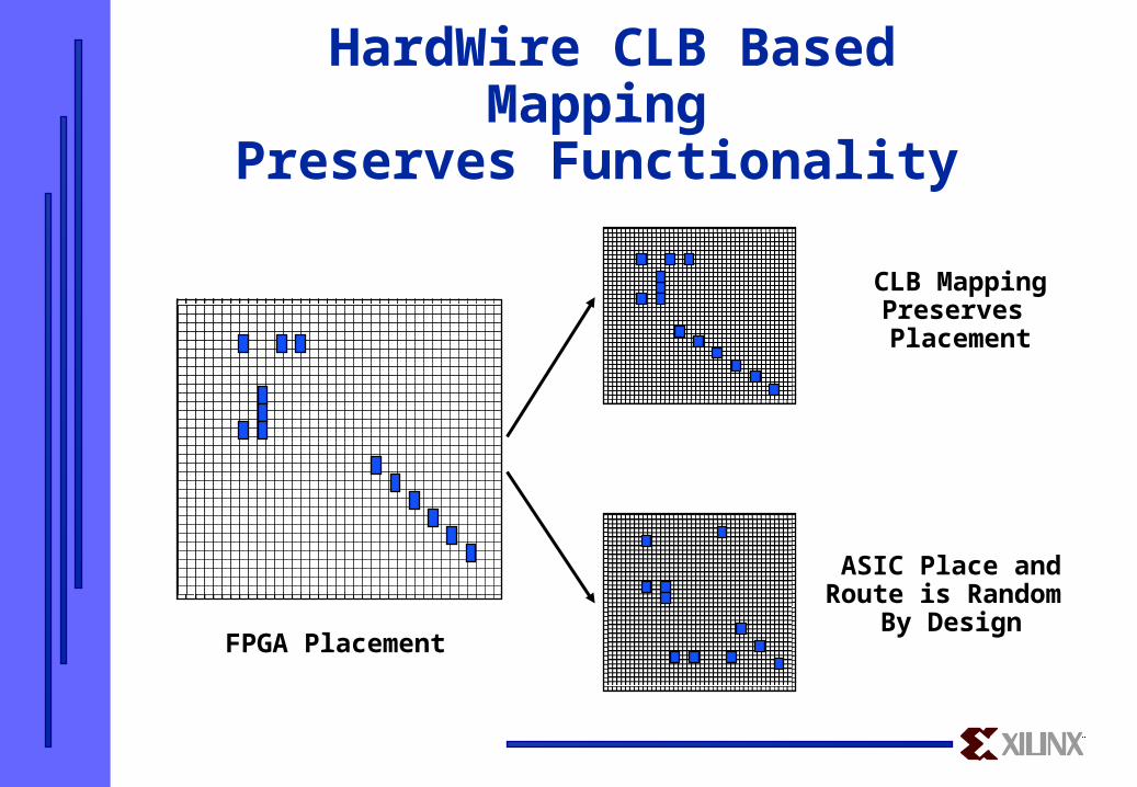
HardWire CLB Based Mapping Preserves Functionality
CLB Mapping Preserves Placement
ASIC Place and Route is Random
By DesignFPGA Placement

FPGA DEVICE ROUTING
Generic ASIC Routing Can Change Critical Paths
HardWire ASIC DesignLocktm Methodology:Placement, Routing and Relative Timing Preserved
DesignLocktm MethodologyMinimizes Change

XH3 Architecture is Xilinx Specific
Efficient Hi-PerformanceASIC Core
FPGA I/O(Driver, ESD,5V Tolerant,JTAG)
PAD
OSC
POR,CE
VREF,CLKS
FPGA Features
Core
Cor
e
FPGA Cores

The Competitive Battleground:Reducing Time to Volume
Iterations (ASIC)
Iterations
Iterations
Iterations
FPGA
FPGA +HardWire ASIC
FPGA +Generic ASIC
Generic ASIC
Iterations (ASIC)
Design/Verification
SystemVerification
ASICRe-engrg.
Prototypes
Production
With Iterations
With Iterations

What is a Prototype?Standard Gate Array vs. the HardWire Array
StandardGate Array
HardWireArray
Wafer FabSpecial quick-turn
fab line (notproduction fab)
Production Fab
Assembly
Opens/Shorts
Productionassembly line
Package Type
Quick-turnassembly line
Production Package
Test
Ceramic
Production Test
Typical gate array prototype is a functional prototype only HardWire Array prototype truly represents the production part

HardWire Success I
Application: Arcade Video Game
FPGA: XC4020E-2PQ208
Features: Dual port RAM, PCI Logicore (Initiator and Target)
Comment: Attempted to do standard ASIC with several manufacturers with no success.
Solution: Only the HardWire ASIC solution was able to incorporate the logic and features providing a cost effective solution.HardWire Device: XC4420-PQ208CProjected Volume: 120-200KU per year.

HardWire Success II
Application: Controller chip in three chip telecom chipset.
FPGA: XC4020E-3PQ208I
Features: Dual port RAM, JTAG and Configuration Emulation.
Comment: Needed fast time to market cost effective solution. Internal solution could not meet time to market requirements.
Solution: HardWire ASIC provided production quality samples 7 weeks after the design submittal kit was received. Including package change.
HardWire Device: XC4420-TQ100C
Projected Volume: 100-300KU per year. Sold to several phone companies

HardWire Success III
Application: six chip encryption chipset for next generation phone/radio base station.
FPGA: XC3030-5PC84I, XC5204-4PQ100, XC4005E-3PQ100.
Features: SelectRAM, JTAG and Configuration Emulation.
Comment: Limited engineering resources available to complete conversion process. Time to completion critical for end customer.
Solution: Used different HardWire technologies to match features and performance with most cost effective solution. Production quality samples delivered 6 weeks after complete design submittal kit received.
HardWire Device: XC3330-PC84I, XC5404-PQ100I, XC4405-PQ100C Projected Volume: 10-20KU per year.

XACT Step M1XACT Step M1
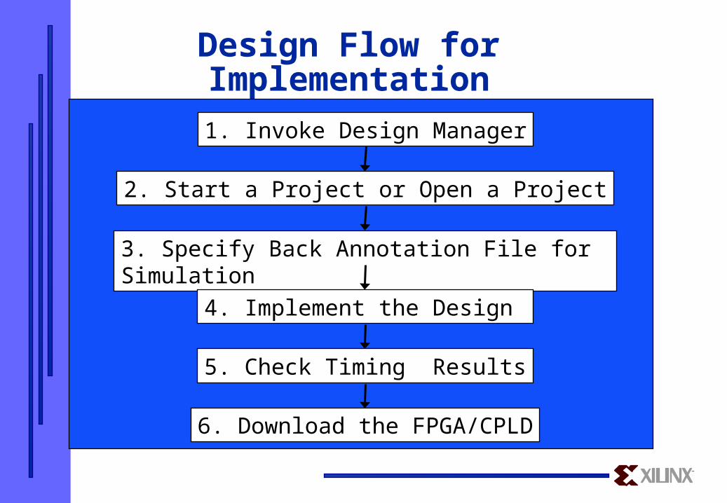
Design Flow for Implementation
1. Invoke Design Manager
2. Start a Project or Open a Project
3. Specify Back Annotation File for Simulation
4. Implement the Design
5. Check Timing Results
6. Download the FPGA/CPLD

Step 1: Invoke Design Manager
Configurable Flow EngineControls start/stop points and custom options
Timing AnalyzerReport on net and path delays
PROM File FormatterCreate file to program configuration file into PROM
Hardware DebuggerDownload configuration file
Design EditorDevice-level view of routing
• Invoke the Design Manager – Command line usage: dsgnmgr <cr>. PC users: select icon
• The Design Manager window appears:
Status Window

Step 2: Start a Project
Set up the design for implementation
Select Part Type
B. Select Part
C. Select Options (...see next foil)
A. Select Design -> Implement

Step 3: Specify Back Annotation
Select Design -> Implement -> Options
Enable “Produce Timing Simulation Data”
Design -> Implement -> Options

Step 3: Specify Back Annotation
Format options:VHDLVerilogXNFEDIF
EDIF formats:Generic - Standard 2000ViewlogicMentor EDIF
• Specify the Back Annotation Netlist Format• To use this form, select Design -> Implement ->
Options -> Edit Implementation Template -> Interface
Design -> Implement -> Options -> Edit Template

Step 4: Implement the Design (1) Select Design -> Implement -> Run
Or press right arrow icon “Run-only” Flow Engine appears
– The design is implemented and the configuration file is created
Flow Engine Status WindowMain Window

Step 4: Implement the Design (2)
The Flow Engine appears after implementation is started
— Allows further customization Tracks status of the design
Flow Engine Status Window

Step 5. Check Results (1) Select Utilities -> Report Browser from the Design Manager
Reports are shown once available Double-click to open Yellow sparkles indicates new (not yet read)
Main Window
Report Browser

Step 5: Check Results (2)
Key Report Files Map Report
Displays result of DRC (Design Rule Check) Indicates if the design will fit into the specified part Identifies ways to improve the design Reports nets with no source or load
Logic Level Timing Report provides delay estimates Created after Map Reports longest paths in the design Created before placement Based on block delays and minimum net delays

Step 5: Check Results (3) Placement and Routing Report includes resource summary
Indicates the percentage of utilization The number of I/O and flip-flops is specified Reports if the design routed Gives an overall timing score
– Score of zero indicates all timing specifications were met
Post Layout Timing Report Based on block delays and net delays after routing Used for detailed delay analysis after implementation
DLY Report Lists delay for each net
Pad Report Cross reference of Input/Output components and package pins
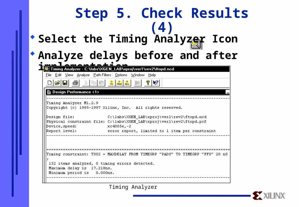
Step 5. Check Results (4)
Select the Timing Analyzer Icon Analyze delays before and after implementation
Timing Analyzer

Step 6: Configure the FPGA/CPLDTo configure, or program FPGAs, a bit file is
downloaded Configuration can be driven by a microprocessor Data can be stored in a PROM
To configure CPLDs, a JED file is downloaded CPLDs can be configured In-System, or CPLDs can be configured using third party programmers
More information on Configuration is given later today


![Debugging Embedded Cores in Xilinx FPGAs [Zynq] · Debugging Embedded Cores in Xilinx FPGAs [Zynq] 2 ©1989-2018 Lauterbach GmbH Debugging Embedded Cores in Xilinx FPGAs [Zynq] Version](https://img.pdfslide.us/doc/110x75/5b7791867f8b9a805c8d49cd/debugging-embedded-cores-in-xilinx-fpgas-zynq-debugging-embedded-cores-in.jpg)