Embed Size (px)
Citation preview
Intrinsic single-domain switching in ferroelectricmaterials on a nearly ideal surfaceS. V. Kalinin†‡§, B. J. Rodriguez†‡, S. Jesse†, Y. H. Chu¶, T. Zhao¶, R. Ramesh¶, S. Choudhury�, L. Q. Chen�, E. A. Eliseev††,and A. N. Morozovska‡‡
†Materials Science and Technology Division and ‡Center for Nanophase Materials Sciences, Oak Ridge National Laboratory, Oak Ridge, TN 37831;¶Department of Physics and Department of Materials Science and Engineering, University of California, Berkeley, CA 94720; �Department ofMaterials Science and Engineering, Pennsylvania State University, University Park, PA 16802; ††Institute for Problems of Materials Science,National Academy of Science of Ukraine, 3, Krjijanovskogo, 03142 Kiev, Ukraine; and ‡‡V. Lashkaryov Institute of Semiconductor Physics,National Academy of Science of Ukraine, 41, pr. Nauki, 03028 Kiev, Ukraine
Communicated by E. Ward Plummer, University of Tennessee, Knoxville, TN, October 2, 2007 (received for review July 6, 2007)
Ferroelectric domain nucleation and growth in multiferroic BiFeO3
is studied on a single-domain level by using piezoresponse forcespectroscopy. Variation of local electromechanical response withdc tip bias is used to determine the size of the domain formedbelow the conductive scanning probe tip. The domain parametersare calculated self-consistently from the decoupled Green functiontheory by using tip geometry determined from the domain wallprofile. The critical parameters of the nucleating domain and theactivation energy for nucleation are determined. The switchingmechanism is modeled by using the phase-field method, andcomparison with experimental results shows that the nucleationbiases are within a factor of �2 of the intrinsic thermodynamiclimit. The role of atomic-scale defects and long-range elastic fieldson nucleation bias lowering is discussed. These measurementsopen a pathway for quantitative studies of the role of a singledefect on kinetics and thermodynamics of first order bias-inducedphase transitions and electrochemical reactions.
phase transition � polarization switching � scanning probe microscopy �piezoresponse force microscopy � BiFeO3
The electrical control of magnetic ordering in multiferroic ma-terials and self-assembled nanostructures has recently propelled
these materials to the forefront of condensed matter physics andmaterials science (1–4). Studies of these systems provide insightinto fundamental mechanisms of coupling between the lattice, spin,and electronic degrees of freedom and resulting order parametersin the bulk and at the interfaces. Furthermore, these systems opena pathway toward device applications including nonvolatile mem-ories (5) and electrically controlled magnetic tunneling junctions,combining nonvolatile electrical writing and magnetic or resistiveread-out schemes (6, 7).
Applications of ferroelectric and multiferroic materials innanoscale devices necessitate the understanding of switchingprocesses in confined and low-dimensional geometries. Becauseof the restrictions imposed by the size of the active region, onlya limited number of domains can nucleate. As the size of thesystem is reduced, the effects of interfaces and structural defectsbecome statistically more significant. Furthermore, novel typesof ferroelectric ordering stabilized by the spatial constraints anddepolarization field effects can emerge (8, 9). Dynamic domainbehavior and nucleation and growth mechanisms in low-dimensional ferroelectrics, including the switching mechanism inthe ideal case, and the role of surfaces, interfaces, and defects inthe thermodynamics and kinetics of elementary processes inpolarization reversal are the keys to these applications.
The development of piezoresponse force microscopy (PFM)has enabled high-resolution (�10 nm) imaging of static domainstructures (10, 11). Beyond imaging applications, PFM can beused to study domain dynamics and polarization switching on thenanoscale. Application of a dc field to a conductive tip results inlocal polarization reversal, while subsequent imaging allowsvisualization of the switched domain. Imaging of the domain size
dependence of the voltage pulse duration and magnitude hasyielded information on domain wall mobilities and disorder inferroelectrics (12) and on domain wall pinning on defects (13,14). However, these studies are time-consuming (several minutesper image), and only relatively large, stable domains can beaddressed (lifetimes of �100 s). Therefore, no information onthe early phases of the switching process, nucleation mecha-nisms, or statistical studies of the switching behavior has beenreported previously.
Early stages of polarization switching in nanoferroelectrics canbe addressed by using piezoresponse force spectroscopy (PFS).PFS measures the local electromechanical hysteresis loops thatrepresent the bias dependence of the local electromechanicalresponse, which is directly related to the size of the domainformed below the tip (15, 16). This approach, in which the atomicforce microscope tip acts as a moving top electrode, is similar tomeasurements using ultra-small capacitors. The electric field islocalized below the tip and, hence, polarization switching be-havior is probed within a small (10–50 nm) volume (17, 18).Therefore, the number of defects affecting switching in thevolume below the tip will necessarily be small, opening thepathway to probing switching behavior in nearly ideal materialsand determining the role of single defects in switching. However,the switching mechanism in PFS and the relationship betweenthe measured signal and switched domain size are significantlymore complex than in the planar capacitor case, necessitating thedevelopment of an appropriate theoretical and experimentalframework for data interpretation and analysis.
Here, we develop a self-consistent approach for probingthermodynamics and kinetics of bias-induced phase transitionsbelow the tip. The quantitative interpretation of PFS dataenables the parameters of domains formed below the tip to beuniquely determined. We implement this approach to studyearly-stage polarization switching in multiferroic BiFeO3. Com-parison with the results of phase-field modeling indicates that theswitching in PFS is close to the intrinsic thermodynamic limit.This methodology can also be applied to other bias-inducedphase transitions that may include material exchange, such aselectrochemical reactions, opening a pathway for studying thesetransformations on a single defect level.
ResultsAs a model ferroelectric system, we have chosen the epitaxialfilms of multiferroic BiFeO3. The high quality of the films
Author contributions: S.V.K. and S.J. designed research; B.J.R., S.C., E.A.E., and A.N.M.performed research; S.J., Y.H.C., T.Z., and R.R. contributed new reagents/analytic tools;S.V.K., B.J.R., S.C., L.Q.C., E.A.E., and A.N.M. analyzed data; and S.V.K. and A.N.M. wrote thepaper.
The authors declare no conflict of interest.
§To whom correspondence should be addressed. E-mail: [email protected].
© 2007 by The National Academy of Sciences of the USA
20204–20209 � PNAS � December 18, 2007 � vol. 104 � no. 51 www.pnas.org�cgi�doi�10.1073�pnas.0709316104
Dow
nloa
ded
by g
uest
on
Dec
embe
r 6,
202
1
ensures a low density of defects such as steps, pinholes, antiphaseboundaries, grain boundaries, or interfacial dislocations, withdefect spacing significantly larger than the probing volume ofPFS. Hence, the properties of the nearly ideal surface in theabsence of mesoscopic defects and mediated only by atomic-scale defects, such as oxygen vacancies, can be studied.
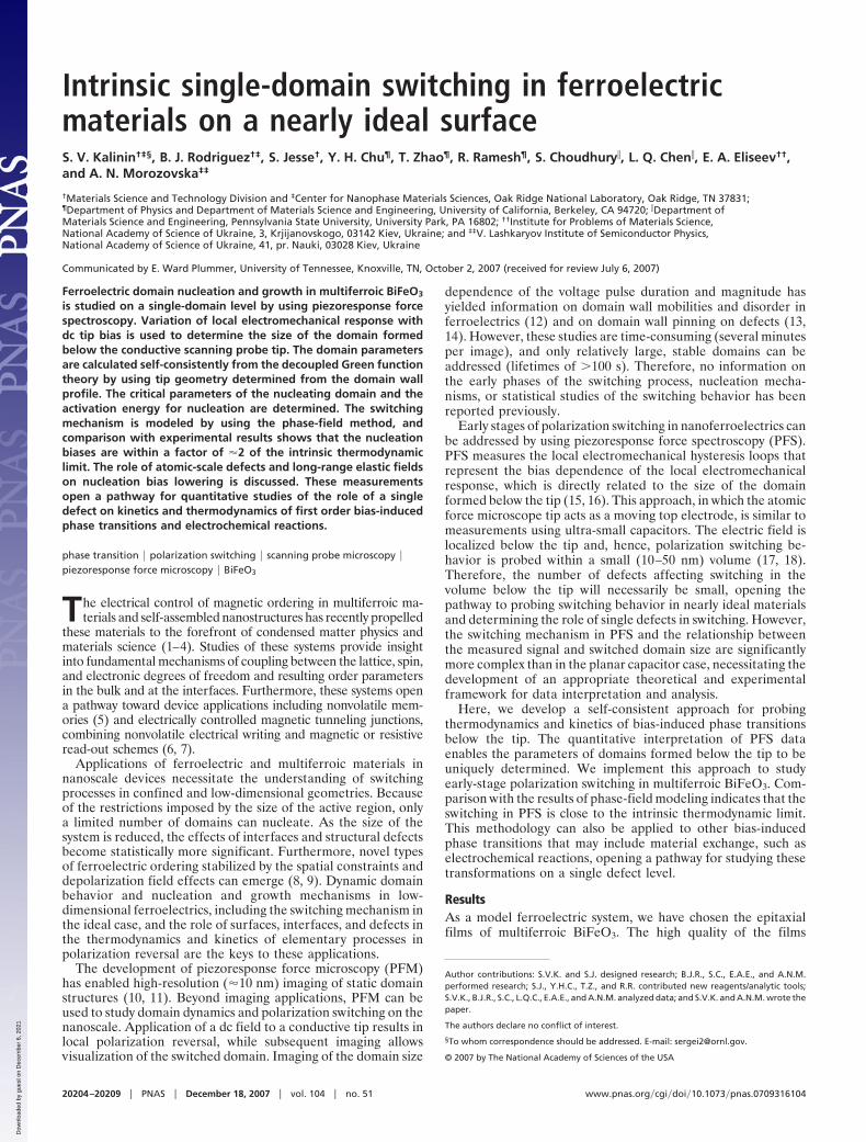
Topographic and PFM images of a BiFeO3 film are shown inFig. 1 a–c. PFS hysteresis loops with different dc bias ranges areshown in Fig. 1d. For a small bias window, the response is linear,whereas for larger biases, the hysteresis loop ‘‘opens up,’’ similarto the macroscopic polarization–electric field (P-E) hysteresisloops (Fig. 1e). The observed evolution of the hysteresis loopssuggests that the domain growth process is limited by domainnucleation below the tip, as evidenced by a fixed response at lowvoltages, and a sudden change above a certain critical bias. Thecoercive biases (corresponding to zero response) determined inthe local PFS measurements [6.5 V for positive, and 9.4 V fornegative (Vc � 8)] are within a factor of two of the macroscopicmeasurements [5 V for positive, and 3 V for negative (Vc � 4)].The asymmetry in the coercive fields arises primarily because ofthe difference of the electrical boundary conditions at themacroscopic bottom (oxide) and local top (gold-coated tip)electrodes. Recent studies (19) on similar samples with thick-nesses from 30 to 2 nm has demonstrated that the asymmetry isalmost thickness-independent and thus can be attributed tocontact behavior. The similarity between PFS data and macro-scopic P-E loops is rather striking given the vastly differentmechanisms (multiple domain switching and growth in themacroscopic case vs. single-domain growth in PFS).
DiscussionThe PFS data represent a convolution between the signalgeneration volume determined by the probe and the size of theforming domain. Quantitative deconvolution requires the solu-tion of two problems: (i) establishment of the relationshipbetween domain parameters and the PFS signal for a known tipgeometry, and (ii) calibration of the tip geometry. Here, we
derive the solution for these problems self-consistently in theframework of the linear decoupled theory of Felten et al. (20).The displacement vector ui(x) at position x, describing tip-biasinduced surface displacement directly below the tip, is
ui�x� � �0
�
d�3���
�
d�2 ���
�
d�1ckjmndlnmEk����Gij�x, ��
�� l,
[1]
where � is the coordinate system related to the material, dlmn arethe piezoelectric coefficients, and ckjmn are the elastic stiffnesses.Ek(�) is the electric field produced by the probe, and Gij(x, �) isthe elastic Green function (21).
The key parameter in the switching process is the character-istic tip size (e.g., the tip radius of curvature or contact radius),which determines the field structure in the material. Here, wedevelop an algorithm to determine the tip size self-consistentlyfrom the observed domain wall width. The electric field pro-duced by the tip is calculated within a framework of an imagecharge model either as a single point charge or a set of pointcharges in a sphere-plane model. For a single point charge,integration of Eq. 1 using the isotropic elastic Green function fora half-plane (21), and Pade analysis of the resulting complexexpression, the domain wall profile is derived as
PR�x� � u0 �34
d*33
x � a0
�x � a0� � d/4�
14
d15
x � a0
�x � a0� � 3d/4. [2]
Here, u0 is the offset accounting for the electrostatic contribu-tion to the signal, and a0 is the center position of the domain wall.The charge parameters (Q, d) are chosen such that (i) thepotential on the surface is equal to the tip bias and (ii) the radiusof curvature of the isopotential surface is equal to R0 at the pointof contact. From these conditions, d � �eR0/� and Q �2��0�eR0U(� � �e)/�, where � is the dielectric constant of the
-12 -8 -4 0 4 8 12-80
-60
-40
-20
0
20
40
60
80
Pol
ariz
atio
n [µ
C/c
m2]
Bias [V]
400 nm
-20 -10 0 10 20
-20
-10
0
10
20
Effe
ctiv
e d 33
[pm
/V]
Bias [V]
PNB
NNB
PCB
NCB
a b c
d e
Fig. 1. Macroscopic and local hysteresis measurements in BiFeO3. (a–c) Surface topography (a), PFM amplitude (b), and phase images (c) of the 200-nm BiFeO3
surface. (d) Local electromechanical hysteresis loops obtained by PFM (at approximate location marked by white dot in a) in comparison with e. (e) P-E hysteresisloops from macroscopic measurements. Both d and e are plotted as a function of voltage applied to the tip (d) or top electrode (e), illustrating close similaritybetween switching biases. The z-scale in a is 20 nm.
Kalinin et al. PNAS � December 18, 2007 � vol. 104 � no. 51 � 20205
PHYS
ICS
Dow
nloa
ded
by g
uest
on
Dec
embe
r 6,
202
1
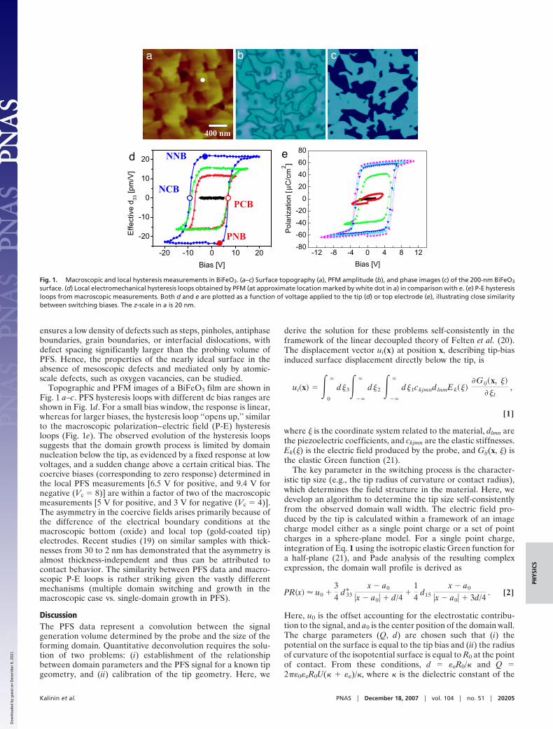
material. Eq. 2 is also applicable to the sphere-plane model of thetip, for which
d � R0
2�e
� � �eln� �e � �
2�e� ,
and R0 is the tip radius of curvature (Fig. 2a).The relative contribution of the magnetoelectric coupling to
the piezoresponse signal is determined by the dimensionlessterm � � �1d�1�, where d are piezoelectric constants, � arepiezomagnetic constants, are linear magnetoelectric constants,and are magnetic permittivities. Estimating d � 50 pm/V, � �10�11 m/A, and 10�10 C/(m2 Oe) (see ref. 22), the constant� � 2 10�7. Hence, the magnetoelectric contribution to thePFM signal can be neglected in antiferroelectric multiferroics.
Because the values of the piezoelectric constants d33, d31, andd15, and Poisson’s ratio, �, for BiFeO3 are not known, we treatd*33 � d33 � (1 � 4�)d31/3 and d15 as fitting parameters. Toaccount for the change in tip-surface contact conditions, thehysteresis data were normalized with respect to the signal on thesaturated portion of the curve, and the ratio d15/d*33 was keptconstant during the fitting. The deconvolution was performedfor both sphere-plane and point charge models, and the resultingdeviation in the domain radii did not exceed a factor of 2.Similarly, the deconvoluted values of charge-surface separation,d, depends on the ratio d15/d*33 only weakly; namely, it varies from13 nm at d15/d*33 � 2 to 18 nm for d15/d*33 � 0.5. The fitting ofseveral domain wall profiles using Eq. 2 yields d � 14 nm andd*33 � d15 � 43.2 pm/V, as shown in Fig. 2b. In the sphere-planemodel, the uncertainty is related to the dielectric constant of thetip-surface medium, and for �e � 81 (‘‘free’’ water), 10 (‘‘bound’’water), and 1 (air), the tip radii were estimated as R0 � 15, 50,
and 200 nm. Despite the difference, the effective electric fielddistribution in these cases is similar, as discussed below.
To determine the domain parameters in PFS, we approximatethe domain as a semiellipsoid of diameter rd and length ld. Thedomain shape is usually elongated (19–22), whereas the tip-generated electric field is generally concentrated on the surface,making the domain radius the critical parameter determining thePFS signal. The relationship between the domain radius and thePFM signal can be determined from Eq. 1 for isotropic dielectricmaterial as
PR�Vdc� � u0 �34
d*33
�d � 8r�d � 8r
�d15
43�d � 8r3�d � 8r
, [3]
where r � r(Vdc) is the voltage-dependent domain radius. Thevoltage dependence of the domain radius deconvoluted from thedata in Fig. 1d is shown in Fig. 2c. Remarkably, we have foundthat the deconvoluted values of domain diameter differ by nomore than �5% for the d15/d*33 ratio varied from 2 to 0.5. Theprimary reason for the insensitivity of the deconvolution pro-cedure to the d15/d*33 ratio or exact tip model (sphere plane, pointcharge) is that the corresponding terms in the domain wallprofile equation and the hysteresis loop equation have a verysimilar structure, so the correction largely cancels out. Similarly,the deconvolution is relatively insensitive to the tip radius or thedielectric constant. In other words, the effective tip size isdirectly related to the measured domain wall width, providing asingle relevant length scale of the problem, which only weaklydepends on the adopted model for tip geometry.
The evolution of the electric field at the domain boundary isshown in Fig. 2d. The field rapidly decreases with domain size,indicative of a decrease in domain-wall curvature. From Fig. 1d,the critical bias for nucleation, corresponding to a bias at which
(a)
25 30 35 40 45
0.6
0.8
1
1.2
1.4
1.6
1.8
0RQde
0 5 10 15 20 25 3010-2
10-1
100
Ele
ctric
fiel
d [M
V/m
]
Tip Bias [V]
0 5 10 150
1
2
3
4
Ea
[eV
]
U [V]
Nucleation
0 5 10 15 20 25 30-20
0
20
40
60
80
100
120
140
Dom
ain
radi
us [n
m]
Tip bias [V]
aε c
Qd
r
l
z
ρϕ
e
25 nm
ε
ε
ε
a b
c d
Fig. 2. Self-consistent measurements of domain size in a PFS experiment. (a) Schematic of the tip interaction with a semiellipsoidal domain. (Inset)High-resolution PFM amplitude image of a domain wall in BiFeO3. (b) Domain wall profile and fit by Eq. 2 for different tip models. The dotted curve is the singlecharge model with d � 14 nm, and solid and dashed curves are the sphere-plane model with R0 � 15, 50, and 200 nm and �e � 81, 10, and 1, respectively. (Inset)Schematic of the model. (c) Domain radius deconvoluted from the hysteresis data in Fig. 1d in the point charge model. (d) Electric field on the domain boundary.(Inset) Activation energy for different models.
20206 � www.pnas.org�cgi�doi�10.1073�pnas.0709316104 Kalinin et al.
Dow
nloa
ded
by g
uest
on
Dec
embe
r 6,
202
1
the PFS signal deviates from the fully saturated signal, is �4–5V at the selected location. The corresponding domain parame-ters estimated from thermodynamic theory (25) are rd � 0.8 nmand ld � 10 nm, and the activation energy for nucleation isestimated to be 1.3 eV. This is in agreement with the recentinvestigation of thermodynamic nucleation in ultra-thin-filmferroelectric capacitors (27). Note that the electric field at theouter domain boundary is 3 108 V/m. In comparison, theintrinsic thermodynamic switching field for BiFeO3 is estimatedto be 1.9 108 V/m. Hence, the electric field at the domain wallat nucleation is close to the anticipated field necessary to induceintrinsic switching, suggesting that this may be the dominantmechanism for domain nucleation at ferroelectric surfaces in theabsence of defects.
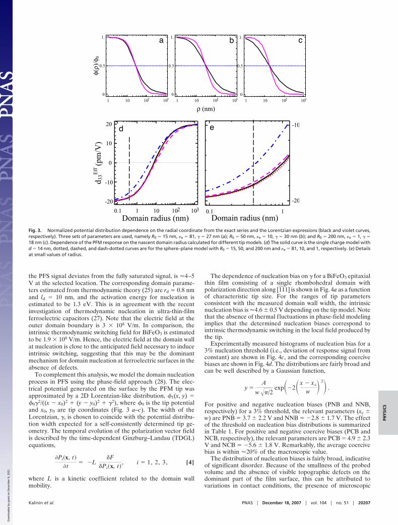
To complement this analysis, we model the domain nucleationprocess in PFS using the phase-field approach (28). The elec-trical potential generated on the surface by the PFM tip wasapproximated by a 2D Lorentzian-like distribution, 1(x, y) � 0�2/((x � x0)2 � (y � y0)2 � �2), where 0 is the tip potentialand x0, y0 are tip coordinates (Fig. 3 a–c). The width of theLorentzian, �, is chosen to coincide with the potential distribu-tion width expected for a self-consistently determined tip ge-ometry. The temporal evolution of the polarization vector fieldis described by the time-dependent Ginzburg–Landau (TDGL)equations,
�Pi�x, t�� t
� �L�F
�Pi�x, t�, i � 1, 2, 3, [4]
where L is a kinetic coefficient related to the domain wallmobility.
The dependence of nucleation bias on � for a BiFeO3 epitaxialthin film consisting of a single rhombohedral domain withpolarization direction along [111] is shown in Fig. 4a as a functionof characteristic tip size. For the ranges of tip parametersconsistent with the measured domain wall width, the intrinsicnucleation bias is �4.6 � 0.5 V depending on the tip model. Notethat the absence of thermal fluctuations in phase-field modelingimplies that the determined nucleation biases correspond tointrinsic thermodynamic switching in the local field produced bythe tip.
Experimentally measured histograms of nucleation bias for a3% nucleation threshold (i.e., deviation of response signal fromconstant) are shown in Fig. 4c, and the corresponding coercivebiases are shown in Fig. 4d. The distributions are fairly broad andcan be well described by a Gaussian function,
y �A
w��/2exp��2� x � xc
w � 2� .
For positive and negative nucleation biases (PNB and NNB,respectively) for a 3% threshold, the relevant parameters (xc �w) are PNB � 3.7 � 2.2 V and NNB � �2.8 � 1.7 V. The effectof the threshold on nucleation bias distributions is summarizedin Table 1. For positive and negative coercive biases (PCB andNCB, respectively), the relevant parameters are PCB � 4.9 � 2.3V and NCB � �5.6 � 1.8 V. Remarkably, the average coercivebias is within �20% of the macroscopic value.
The distribution of nucleation biases is fairly broad, indicativeof significant disorder. Because of the smallness of the probedvolume and the absence of visible topographic defects on thedominant part of the film surface, this can be attributed tovariations in contact conditions, the presence of microscopic
0.1 1 10 102 103
-20
-10
0
10
20
Domain radius (nm)
d 33E
ff (
pm/V
)
0.1 1
-20
-10
Domain radius (nm)
(b)
1 10 102 1030
0.5
1.
1 10 102 1030
0.5
1.
1 10 102 1030
0.5
1.
ρ (nm)
φ(ρ)
/φ0
a b c
d e
Fig. 3. Normalized potential distribution dependence on the radial coordinate from the exact series and the Lorentzian expressions (black and violet curves,respectively). Three sets of parameters are used, namely R0 � 15 nm, �e � 81, � � 27 nm (a); R0 � 50 nm, �e � 10, � � 30 nm (b); and R0 � 200 nm, �e � 1, � �18 nm (c). Dependence of the PFM response on the nascent domain radius calculated for different tip models. (d) The solid curve is the single charge model withd � 14 nm, dotted, dashed, and dash-dotted curves are for the sphere–plane model with R0 � 15, 50, and 200 nm and �e � 81, 10, and 1, respectively. (e) Detailsat small values of radius.
Kalinin et al. PNAS � December 18, 2007 � vol. 104 � no. 51 � 20207
PHYS
ICS
Dow
nloa
ded
by g
uest
on
Dec
embe
r 6,
202
1
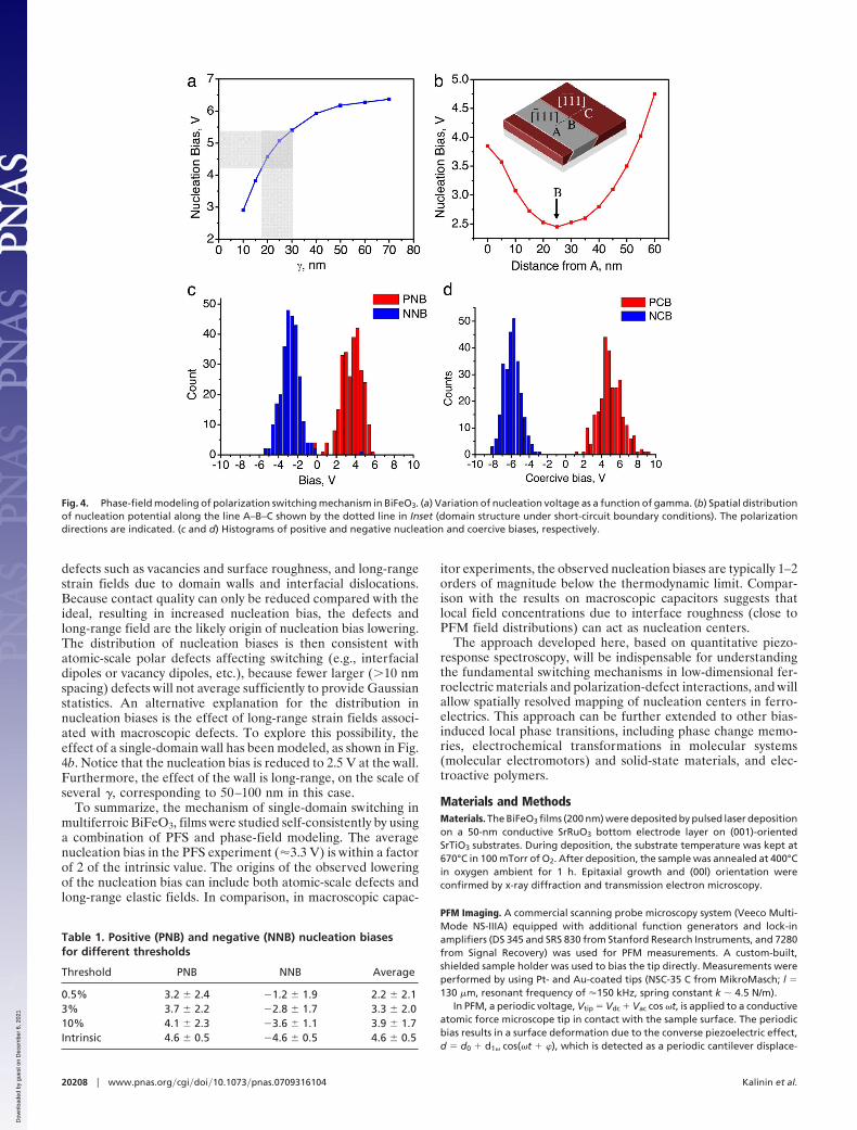
defects such as vacancies and surface roughness, and long-rangestrain fields due to domain walls and interfacial dislocations.Because contact quality can only be reduced compared with theideal, resulting in increased nucleation bias, the defects andlong-range field are the likely origin of nucleation bias lowering.The distribution of nucleation biases is then consistent withatomic-scale polar defects affecting switching (e.g., interfacialdipoles or vacancy dipoles, etc.), because fewer larger (�10 nmspacing) defects will not average sufficiently to provide Gaussianstatistics. An alternative explanation for the distribution innucleation biases is the effect of long-range strain fields associ-ated with macroscopic defects. To explore this possibility, theeffect of a single-domain wall has been modeled, as shown in Fig.4b. Notice that the nucleation bias is reduced to 2.5 V at the wall.Furthermore, the effect of the wall is long-range, on the scale ofseveral �, corresponding to 50–100 nm in this case.
To summarize, the mechanism of single-domain switching inmultiferroic BiFeO3, films were studied self-consistently by usinga combination of PFS and phase-field modeling. The averagenucleation bias in the PFS experiment (�3.3 V) is within a factorof 2 of the intrinsic value. The origins of the observed loweringof the nucleation bias can include both atomic-scale defects andlong-range elastic fields. In comparison, in macroscopic capac-
itor experiments, the observed nucleation biases are typically 1–2orders of magnitude below the thermodynamic limit. Compar-ison with the results on macroscopic capacitors suggests thatlocal field concentrations due to interface roughness (close toPFM field distributions) can act as nucleation centers.
The approach developed here, based on quantitative piezo-response spectroscopy, will be indispensable for understandingthe fundamental switching mechanisms in low-dimensional fer-roelectric materials and polarization-defect interactions, and willallow spatially resolved mapping of nucleation centers in ferro-electrics. This approach can be further extended to other bias-induced local phase transitions, including phase change memo-ries, electrochemical transformations in molecular systems(molecular electromotors) and solid-state materials, and elec-troactive polymers.
Materials and MethodsMaterials. The BiFeO3 films (200 nm) were deposited by pulsed laser depositionon a 50-nm conductive SrRuO3 bottom electrode layer on (001)-orientedSrTiO3 substrates. During deposition, the substrate temperature was kept at670°C in 100 mTorr of O2. After deposition, the sample was annealed at 400°Cin oxygen ambient for 1 h. Epitaxial growth and (00l) orientation wereconfirmed by x-ray diffraction and transmission electron microscopy.
PFM Imaging. A commercial scanning probe microscopy system (Veeco Multi-Mode NS-IIIA) equipped with additional function generators and lock-inamplifiers (DS 345 and SRS 830 from Stanford Research Instruments, and 7280from Signal Recovery) was used for PFM measurements. A custom-built,shielded sample holder was used to bias the tip directly. Measurements wereperformed by using Pt- and Au-coated tips (NSC-35 C from MikroMasch; l �130 m, resonant frequency of �150 kHz, spring constant k 4.5 N/m).
In PFM, a periodic voltage, Vtip � Vdc � Vac cos �t, is applied to a conductiveatomic force microscope tip in contact with the sample surface. The periodicbias results in a surface deformation due to the converse piezoelectric effect,d � d0 � d1� cos(�t � �), which is detected as a periodic cantilever displace-
Fig. 4. Phase-field modeling of polarization switching mechanism in BiFeO3. (a) Variation of nucleation voltage as a function of gamma. (b) Spatial distributionof nucleation potential along the line A–B–C shown by the dotted line in Inset (domain structure under short-circuit boundary conditions). The polarizationdirections are indicated. (c and d) Histograms of positive and negative nucleation and coercive biases, respectively.
Table 1. Positive (PNB) and negative (NNB) nucleation biasesfor different thresholds
Threshold PNB NNB Average
0.5% 3.2 � 2.4 �1.2 � 1.9 2.2 � 2.13% 3.7 � 2.2 �2.8 � 1.7 3.3 � 2.010% 4.1 � 2.3 �3.6 � 1.1 3.9 � 1.7Intrinsic 4.6 � 0.5 �4.6 � 0.5 4.6 � 0.5
20208 � www.pnas.org�cgi�doi�10.1073�pnas.0709316104 Kalinin et al.
Dow
nloa
ded
by g
uest
on
Dec
embe
r 6,
202
1
ment at the excitation frequency, �. The tip is scanned maintaining constanttip-surface force (topographic feedback) to generate images of piezoresponseamplitude, d1�, and piezoresponse phase, �. The amplitude is proportional tolocal electromechanical activity, while the phase is 0° for domains with P�n �0 and 180° for P�n � 0, where P is the polarization vector and n is the unitnormal.
PFM Spectroscopy and SS-PFM. In PFS, the electromechanical response ismeasured as a function of tip dc bias, Vdc, applied before measurement (16).Application of sufficiently high constant bias results in the nucleation andsubsequent growth of domains of opposite polarity below the tip, with aconcurrent change of the PFM signal from PR (initial state) to �PR (switchedstate). The resulting PR(Vdc) dependence contains information on domainnucleation and growth below the tip. In switching spectroscopy PFM (SS-PFM),the hysteresis loops are acquired at each point in an N N grid (typicallyn � 32 � 128) that is further analyzed to yield 2D maps of switching param-eters such as the positive and negative nucleation biases and the work ofswitching (29).
To analyze the statistical distribution of switching biases within the film, wehave developed automatic routines for analysis of multiple (102 � 104) hys-teresis loops based on a phenomenological fitting function method (30). Thenucleation bias is determined as a voltage corresponding to the deviation ofthe electromechanical response from the remanent value by a predefinedvalue. To establish reliable criterion for domain nucleation onset in the PFSdata analysis, the electromechanical response was calculated by using Eq. 3 asa function of domain radius for different tip models. The changes in theelectromechanical response as a function of domain radius are shown in Fig.3 d and e. For a 0.4-nm domain, the deviations are 10.6%, 10.0%, 12.1%, and23.3% (solid, dotted, dashed, and dash-dotted curves, respectively) for differ-ent models. For a 1-nm domain, deviations are 24.5%, 23.2%, 26.2%, and45.3% (solid, dotted, dashed, and dash-dotted curves, respectively). Thisstrong dependence of signal on domain size even at the early stages ofswitching is a direct consequence of the 1/r dependence of the correspondingGreen function. Realistic nucleation thresholds will be lower because thedomain geometry at the early stages is hemispherical, rather than cylindrical,
and the mechanical contact area is finite. Hence, we use threshold values of0.5%, 3%, and 10% to account for these effects, and establish the sensitivityof analysis for a chosen threshold value.
Phase-Field Modeling. Eq. 4 is solved numerically by using the semiimplicitFourier spectral method (31). In the simulations, we used a model of 128 x 128 x 32 x, with periodic boundary conditions along x1 and x2 axes in thefilm plane, where x is the simulation grid spacing. The thickness of the filmis taken as hf � 16 x. The dielectric stiffness used to calculate the bulk energyalong with the elastic and electrostrictive coefficients used in elastic energycalculation are obtained from ref. 31. For elastic energy calculations, weassumed that the substrate exerts a biaxial compressive strain of 1% on thethin film. The gradient energy coefficients were chosen as G11/G110 � 0.4.Because of the dearth of experimental values of domain wall width anddomain wall energy for the BiFeO3 system, the width of the 180° domain walland the corresponding domain wall energy were taken to be similar inmagnitude to other perovskite ferroelectric systems (32). For electrostaticenergy calculations, we used �11 � �22 � �33 � 100. Effective tip size, �, is variedfrom 10 nm to 70 nm in 10-nm steps. The pristine state was chosen as a singlerhombohedral domain with polarization along [111]. To find the criticalnucleation potential, the potential 0 was gradually increased with an incre-ment of 0.05 V, and the domain structure from a previous simulation was usedas the input at each increment of the potential. At a critical applied electricpotential, a new rhombohedral domain with polarization along [111] wasfound to nucleate below the tip, and the corresponding electric potential wasidentified as the nucleation potential.
ACKNOWLEDGMENTS. We gratefully acknowledge valuable discussions withE. Ward Plummer (University of Tennessee/Oak Ridge National Laboratory).This work was supported by the Division of Materials Sciences and Engineer-ing, Oak Ridge National Laboratory, managed and operated by UT-Battellefor the Office of Basic Energy Sciences, U.S. Department of Energy (S.V.K.,B.J.R., and S.J.); the U.S. Department of Energy under Contract DE-FG02-07ER46417 (S.C. and L.Q.C.); and the Director, Office of Science, Office of BasicEnergy Sciences, Division of Materials Sciences and Engineering, U.S. Depart-ment of Energy under Contract DE-AC02-05CH11231 (Y.H.C., T.Z., and R.R.).
1. Ederer C, Spaldin NA (2004) Nat Mater 3:849–851.2. Lottermoser T, Lonkai T, Amann U, Hohlwein D, Ihringer J, Fiebig M (2004) Nature
430:541–544.3. Wang J, Neaton JB, Zheng H, Nagarajan V, Ogale SB, Liu B, Viehland D, Vaithyanathan
V, Schlom DG, Waghmare UV, et al. (2003) Science 299:1719–1722.4. Eerenstein W, Mathur ND, Scott JF (2006) Nature 442:759–765.5. Hur N, Park S, Sharme PA, Ahn JS, Guha S, Cheong SW (2004) Nature 429:392–395.6. Gajek M, Bibes M, Fusil S, Bouzehouane K, Fontcuberta J, Barthelemy A, Fert A (2007)
Nat Mater 6:296–302.7. Eerenstein W, Morrison FD, Scott JF, Mathur ND (2005) Appl Phys Lett 87:101906.8. Gorbatsevich AA, Kopaev YV (1994) Ferroelectrics 161:321–334.9. Naumov II, Bellaiche L, Fu HX (2004) Nature 432:737–740.
10. Gruverman A, Kholkin A (2006) Rep Prog Phys 69:2443–2574.11. Kim S, Gopalan V, Gruverman A (2002) Appl Phys Lett 80:2740–2742.12. Tybell T, Paruch P, Giamarchi T, Triscone JM (2002) Phys Rev Lett 89:097601.13. Paruch P, Giamarchi T, Triscone JM (2005) Phys Rev Lett 94:197601.14. Agronin A, Rosenwaks Y, Rosenman G (2006) Appl Phys Lett 88:072911.15. Wu A, Vilarinho PM, Shvartsman VV, Suchaneck G, Kholkin AL (2005) Nanotechnology
16:2587–2595.16. Alexe M, Harnagea C, Hesse D, Gosele U (2001) Appl Phys Lett 79:242–244.17. Gruverman A, Rodriguez BJ, Dehoff C, Waldrep JD, Kingon AI, Nemanich RJ, Cross JS
(2005) Appl Phys Lett 87:082902.
18. Stolichnov I, Malin L, Colla E, Tagantsev AK, Setter N (2005) Appl Phys Lett86:012902.
19. Chu YH, Zhao T, Cruz MP, Zhan Q, Yang PL, Martin LW, Huijben M, Yang CH, ZavalicheF, Zheng H, Ramesh R (2007) Appl Phys Lett 90:252906.
20. Felten F, Schneider GA, Munoz Saldana J, Kalinin SV (2004) J Appl Phys 96:563–568.21. Landau LD, Lifshitz EM (1976) Theory of Elasticity, Theoretical Physics (Butterworth-
Heinemann, Oxford), Vol. 7.22. Zvezdin AK, Pyatakov AP (2004) Phys Usp 47:416–421.23. Molotskii M (2003) J Appl Phys 93:6234–6237.24. Abplanalp M, (2001) PhD Thesis (Swiss Federal Institute of Technology, Zurich).25. Morozovska AN, Eliseev EA (2006) Phys Rev B 73:104440.26. Emelyanov YA (2005) Phys Rev B 71:132102.27. Jo JY, Kim DJ, Kim DJ, Choe SB, Song TK, Yoon JG, Noh TW (2006) Phys Rev Lett
97:247602.28. Zhang JX, Li YL, Wang Y, Liu ZK, Chen LQ, Chu YH, Zavaliche F, Ramesh R (2007) J Appl
Phys 101:114105.29. Jesse S, Baddorf AP, Kalinin SV (2006) Appl Phys Lett 88:062908.30. Jesse S, Lee HN, Kalinin SV (2006) Rev Sci Instrum 77:073702.31. Chen LQ, Shen J (1998) Comput Phys Commun 108:147–158.32. Chen YB, Katz MB, Pan XQ, Das RR, Kim DM, Baek SH, Eom CB (2007) Appl Phys Lett
90:072907.
Kalinin et al. PNAS � December 18, 2007 � vol. 104 � no. 51 � 20209
PHYS
ICS
Dow
nloa
ded
by g
uest
on
Dec
embe
r 6,
202
1


![A constitutive model for ferroelectric polycrystalslandis/Landis/Research_files/JMPS1999.pdfferroelectric switching] crystal plasticity theory as developed by Hill "0855# and employed](https://img.pdfslide.us/doc/110x75/61093046ab062728a77912c3/a-constitutive-model-for-ferroelectric-landislandisresearchfilesjmps1999pdf.jpg)