Embed Size (px)
Citation preview
Intrinsic limits on electron mobility in disordereddilute nitride semiconductor alloys
S. Fahy, A. Lindsay and E.P. O’Reilly
Abstract: The authors have previously shown that there is a fundamental connection between thecomposition-dependence of the conduction-band-edge energy and the n-type carrier scatteringcross-section in dilute alloys, imposing general limits on the electron mobility in Ga(In)NAs alloysand heterostructures. A simple general expression is derived for scattering in the ultra-diluteregime, showing that the scattering rate is proportional to jdEc/dxj2, the square of the initialvariation of the conduction-band-edge energy with alloy composition x. The mobility estimated inGaNxAs12x using the two-level band-anti-crossing (BAC) model is of the right magnitude(,1000 cm2/Vs), but still larger than typical experimental values. The effects of N clusters andinhomogeneous broadening of energy levels are considered, including the formation of N–N pairs(where a single Ga atom has two N neighbours) and more complex clusters. It is shown that suchcomplexes play a major role in further limiting the mobility, giving values of 200–400 cm2/Vs, inclose agreement with experiment. It is concluded that random alloy scattering, rather than filmquality or other factors, dominates the carrier mobility in these materials.
1 Introduction
There is considerable interest in dilute nitride alloys, bothbecause of their fundamental physical properties andpotential device applications. When a small fraction of Asatoms in Ga(In)As are replaced by N, the energy gapdecreases rapidly, e.g. by about 150 meV when 1% of N isadded to GaAs [1]. This opens up the possibility of 1.3 and1:5 mm telecomm lasers based on GaAs [2, 3], and also ofextending the wavelength range of GaAs-based solar cellsfurther into the infrared [4]. There has been substantialprogress in understanding many of the properties of dilutenitrides and related alloys. Much of this understanding isbased on the band anti-crossing model developed by Shanet al. [5], who used hydrostatic pressure techniques to showthat the reduction in energy gap can be described by aninteraction between the conduction band edge and a higher-lying set of localised nitrogen resonant states. This andalternative models have provided significant insight intothese novel materials [6–8]. However, until very recently[9, 10] there has been little progress in developing models todescribe their transport and mobility properties. Even foridealised random alloy crystals, these properties are difficultto analyse precisely because N introduces such a strongperturbation to the band structure of Ga(In)As. This mustlead to strong alloy scattering.
In an earlier paper [9], we used an S-matrix formalism toshow that the scattering cross-section for an isolatedimpurity is given by
s ¼ p4
m�
2p�2
� �2 dEc
dx
� �2
a60 ð1Þ
where dEc=dx is the derivative of the band-edge energywith respect to the atomic concentration x of defects in thematerial at very low defect density, m� is the electroneffective mass and a0 is the GaAs lattice constant. Weemphasise that this result is completely general for anylocalised perturbation, whether it be a substitutionalimpurity, alloying atom or any other kind of defect, andis independent of any details of how the perturbation isformed. We note a few caveats regarding (1). First, itassumes that DV is localised compared to the typicaldistances between impurities. Thus, long-range strain fields,which are included in the band energy shift, may notcontribute to the scattering at moderate impurity densities.Secondly, we need to know dEc=dx and not just the bandgapvariation, dEg=dx; in order to apply (1). We shall see belowthat neither of these issues is critical when consideringscattering in ultra-dilute nitride alloys.
2 Ultra-dilute nitride alloys
In an analysis that ignored any N complexes [9], assumingthat all nitrogen is incorporated on single, noninteractinggroup V sites, we estimated that the n-type carrier mobilitym is determined by
m�1 ¼ffiffiffiffiffiffiffiffiffiffiffiffiffiffi3m� kTp
ep
m�
2p�2
� �2 dEc
dx
� �2
a30x ð2Þ
where x is the N atomic concentration in the material, T isthe absolute temperature, k is Boltzmann’s constant and ethe magnitude of the electron charge. Given the experimen-tal values of m� and dEc=dx for GaNxAs1�x; alloy scatteringby single N sites is then found to limit the maximummobility in dilute nitrides to a value of the order of2000 cm2=Vs at room temperature, for x � 0:01–0:02:We note that this mobility is substantially less than the
q IEE, 2004
IEE Proceedings online no. 20040876
doi: 10.1049/ip-opt:20040876
The authors are with NMRC, University College Cork, Lee Maltings,Prospect Row, Cork, Ireland. S. Fahy is also with the Department ofPhysics, University College Cork
Paper received 21st May 2004
IEE Proc.-Optoelectron., Vol. 151, No. 5, October 2004352
ideal mobility of GaAs at room temperature (limitedprincipally by phonon scattering), so that this alloyscattering would then be the dominant limiting factor onthe mobility in the best quality GaNxAs1�x samples.
Both theory and experiment have shown, in the ultra-dilute limit, that an isolated single substitutional N atomintroduces a resonant defect level above the conductionband edge in GaNxAs1�x (about 1.65 eV above the GaAsvalence band maximum) [5, 6, 8, 11, 12], while a N–N pairintroduces a defect level close to the conduction band edge(1.51 eV above the GaAs valence band maximum) [12].In the band-anti-crossing (BAC) model [5], these resonantdefect levels interact with the host material conduction bandedge, leading to the observed rapid reduction in energy gapwith increasing N composition. By contrast, the addition ofH to GaNxAs1�x leads to the formation of N–H complexes,which passivate the effect of the N-related states, with theenergy gap of GaNxAs1�x : H returning to that of GaAs forcomplete passivation of the N-related levels [13–15].Preferential (non-random) pairing of N atoms is notexpected on energetic grounds but, for example, a randomdistribution of N atoms on 1% of the group-V sites inGaN0:01As0:99 will place approximately 12% of the N atomsin N–N pairs since each atom has 12 second-nearestneighbour atoms in the GaAs crystal structure. At thisnitrogen concentration there are also more complex nitrogenclusters. (A cluster is defined as a group of nitrogen atoms,substituting on As sites, which are linked to each otherthrough shared Ga nearest neighbours.)
Single and paired N states give rise to strongly resonantscattering of electrons in the lower conduction band statesof GaAs and GaInAs. In the BAC model [5], this is due tothe presence of the resonant quasi-localised defect levelapproximately 150 meV above the conduction band edge.The strength of any scattering centre is strongly affectedby the energy difference between the resonant state andthe conduction band edge. We noted above that a N–Npair gives rise to a localised level, which is very closeto the unperturbed GaAs conduction band edge. Thisconsiderably increases the level repulsion between theN– N defect state and the conduction band edge,substantially increasing dEc=dx due to this paired defectlevel, compared to the effect of two single-N levels. Atzero temperature and ultra-dilute nitrogen concentrations,the energy of the N–N pair defect is almost identical tothe band edge energy [12].
In an earlier paper [10], we considered the effects of threetypes of N complex on the bandgap and carrier scattering:(a) single, unpassivated, substitutional N atoms; (b) N–Npairs (i.e. where both N atoms share a common Ga nearestneighbour); and (c) hydrogen-passivated N defects. Weassumed independent scattering from each type of centre inthe alloy and that each type of scattering centre had a single,well defined energy, i.e. no inhomogeneous broadening ofquasilocalised levels associated with each defect type.Although in the ultra-dilute limit N–N pairs give rise tolocalised levels almost degenerate with the band edge, wefound that the scattering from these centres gave a relativelysmall modification to the mobility, compared with isolatedsubstitutional nitrogen levels.
When there are several different types of N-complex inthe material, each type in an independent scatteringapproximation contributes in proportion to its concentration,both to the conduction band shift and to the inversemobility. If we consider d different types of complex, eachwith concentration xi; then the bandgap shift DEc and theinverse mobility m�1 will be given by the weighted averageof the individual contributions:
DEc ¼Xd
i¼1
Z@Ec
@xi
dxi ð3Þ
and
m�1 ¼ffiffiffiffiffiffiffiffiffiffiffiffiffiffi3m� kTp
ep
m�
2p�2
� �2Xd
i¼1
@Ec
@xi
� �2
xia30 ð4Þ
We note that, if the bandgap variation with N composition isfitted by assuming a single type of environment (in whichcase dEc=dx is taken as a weighted average of dEc=dxi forthe different types of N centre actually present in thesystem), then the inverse mobility will be underestimated.(This follows simply because the square of the mean ofseveral distinct numbers is always greater than the mean ofthe numbers squared.) This will have important conse-quences when we come to consider the effects of nitrogenclusters and inhomogeneous broadening of localised levels.
In this paper, we extend the previous analyses andexplicitly treat the effects of inhomogeneous broadening ofN defect levels, including the random formation of statesassociated with clusters of two or more N atoms. To do this,we use a supercell approach to calculate the localised Nenergy levels and their interaction with the conduction band.We randomly substitute N atoms on As sites in a largesupercell (containing typically �105 –107 GaAs unit cells)and find the set of localised wave functions and energylevels associated with these N atoms, including any Nclustering effects, within the linear combination of isolatednitrogen states (LCINS) representation [16].
3 LCINS approach
In the LCINS approach, we start with a sp3s� tight-bindingrepresentation [8, 17] of a moderately large supercell(several hundred GaAs unit cells), with one N atomsubstituting (at site i) for one of the As atoms. (Tight-binding parameters have been determined to give a goodrepresentation of the conduction band states in both GaAsand GaN and intermediate structures [18]. The relaxation ofatomic positions is calculated using the GULP moleculardynamics package [19].) The GaAs conduction-band-edgestate j pi is perturbed by the presence of the N atom at site i,so that the exact eigenstate of the system is j pi þ ajN; ii;where jN; ii is orthogonal to j pi: To represent the localisedstates near the conduction band edge in the large supercell,we use a linear combination of the functions jN; ji; wherethe N atoms are at sites j throughout the system. When twoN atoms, on sites l and k, share a common Ga nearestneighbour, the symmetric ‘bonding’ combination of thestates is calculated from the full tight-binding representationand used as a localised basis state in the representation ofcarrier states in the alloy. (The anti-bonding combination isnot included as its coupling to the conduction band edge iszero.) Matrix elements of the Hamiltonian and the overlapbetween states jN; ii; jN; ji and j pi are calculated exactlyfrom the tight-binding representation, so that the full tight-binding Hamiltonian is projected exactly onto a smallersubspace, and the method is formally a restricted variationalrepresentation of states near the conduction band edge.Calculations for supercells containing several hundredGaAs primitive unit cells, substituting N atoms on a rangeof As sites, demonstrate that the wavefunctions and energiesobtained in the LCINS representation closely match thestates near the conduction band edge in the full tight-bindingrepresentation [16]. This close match of the energy levelsimplies that the carrier scattering cross-section of each
IEE Proc.-Optoelectron., Vol. 151, No. 5, October 2004 353
cluster, calculated in the reduced LCINS representation,matches the cross-section calculated in the full tight-bindingrepresentation. Recent calculations [20] using this approachhave predicted the N-concentration-dependence of theconduction band effective mass in excellent agreementwith experiment.
Excluding the conduction band states j pi for the moment,we diagonalise the reduced Hamiltonian for the localisedstates. This gives us a spectrum of states jL; ji;with energiesEj and interaction matrix elements with the conduction bandhL; jjci ¼ bj=
pNa; where Na is the number of group-V sites
in the system. We treat each of these levels as beingassociated with an independent N cluster in the system andcalculate its contribution to the carrier scattering rate.
In the LCINS approach, a cluster may have severallocalised states, but we expect that only one will contributestrongly to the scattering of conduction electrons. Inter-action between cluster states is assumed to be very weak(by definition of a cluster), giving rise to an inhomogeneousbroadening of the localised state energy for each clusterdue to its environment and the other nitrogen atoms nearby.This is reflected in the spectrum of localised states found inthe LCINS calculations.
Two identical localised cluster states will hybridise intosymmetric and antisymmetric linear combinations, even iftheir interaction is very weak, giving rise to one state with acoupling
p2 times the single cluster interaction and another
with zero coupling to the conduction bands. When this isused in the calculation of scattering, the cross-section isproportional to b4 (see (5), below) and so the scatteringcalculated, considering each hybridised state as an inde-pendent scatterer, is twice what one would obtain withoutthe hybridisation. This result is not physically correct,because the two clusters in the material are statisticallyindependent and their scattering intensities, rather than theiramplitudes, should be added.
In a large LCINS supercell calculation, many suchinteractions between physically similar clusters give rise tolocalised states with energies very close to each other, butwith a wide range of conduction band interaction matrixelements due to random hybridisation between the states onthe various clusters. To approximate the physically correctresult (which takes each cluster’s independent contributionto the scattered wave intensity), we average b2 (the squareof the conduction band matrix element) for all localisedstates with energies over a small energy window, of width1 meV. (In practice, widths between 0.2 meV and 5 meVgive very similar results.) We then assume that one localisedstate corresponds to each physically separate cluster and thatall cluster states within that window have the same value ofb2; equal to the average of b2 over the hybridised stateswithin the energy window.
Each localised state jL; ii interacts with the alloyconduction band states jci; which are linear combinationsof the original GaAs conduction band states j pi and theother localised states in the system: jci ¼ Sph pjcijpi þSj6¼iAjjL; ji; where jAjj2 is the weight of the localised statejL; ji in the exact states of the system. If momentumconservation is still a reasonably good approximation, the
conduction band weights jhpjcij2 will be concentrated on asingle value of p for each state jci; or at least in a very smallrange of energies. The total sum of conduction band stateweights is fG ¼ Spjhpjcij2 ¼ 1� SjjAjj2: In such a system,each individual localised state interacts with these deloca-lised states jci; which are linear combinations of conductionband states and the other localised states. Since localisedstates couple only to the original conduction band states j pi;
the interaction matrix element with jci is reduced to b2fG:However, the density of states is increased by a factor of½dE=dEðpÞ��1 ¼ 1=fG; leaving the resonance width Gi
unchanged.In summary, we treat the carrier scattering rate by
multiple, independent localised states as a sum of the ratesfrom individual localised states, but allow for the changein effective matrix element b0 ¼ b
pfG and effective mass
m� ¼ m�0=fG; of delocalised band states, which correspondsto the change in density of states D0ðE0Þ ¼ DðEÞ=fG: Thevalue of the conduction band minimum Ec is alsosubstantially changed (the bandgap reduction with nitrogenconcentration). Values for Ec and fG are found bydiagonalisation of the Hamiltonian for very large supercellsin the LCINS representation, including the GaAs conduc-tion-band-edge state jpi and its interaction with all thelocalised states. The state jci with maximum weight fG onthe original conduction-band-edge state jpi is identified asthe conduction-band-edge state in the dilute alloy and fG isassumed to be energy-independent for the thermally excitedcarrier states.
The scattering rate can then be written as a sum, RðEÞ ¼SiRiðEÞ; over all the localised states in the system. Using thestandard result for resonant scattering [21], the rate for eachlocalised state jL; ii can be written in terms of the scatteringcross-section siðEÞ for that state
RiðEÞ ¼vðEÞsiðEÞ
volume
¼ vðEÞ 4pNaa3
0=4
m�
2p�2
� �2 b4i =N2
a
ðE � EiÞ2 þ G2i
Na
a30
4
� �2
¼ pvðEÞNa
m�
2p�2
� �2
a30
b4i
ðE � EiÞ2 þ G2i
ð5Þ
where vðEÞ ¼ @E=@p is the speed (group velocity) associ-ated with delocalised states of energy E, b0i is the effectiveinteraction strength, Ei the resonance peak energy and Gi theresonance energy halfwidth for localised state i.
In the relaxation time approximation, the Boltzmanntransport equation gives the following result for the currentdensity j due to an electric field F:
j ¼ � 2e2�3
ð2pÞ3Z
1
RðEðpÞÞF � Hpf0ðpÞvðpÞd3p ð6Þ
where R(E) is the relaxation rate for the distribution atenergy E (equal to the alloy carrier scattering rate in thepresent case), f0 is the thermal distribution of carriers inthe states, p is the momentum label of the states and vðpÞ ¼HpEðpÞ is the carrier velocity for momentum p. Assuming aparabolic energy dispersion, EðpÞ ¼ Ec þ p2=2m�; near theband minimum, the current density for an isotropic materialcan then be rewritten as
j ¼ � 2e2F�3
3ð2pÞ3Z 1
0
p2
m�2
RðEÞ@f0
@E4pp2dp ð7Þ
The carrier mobility is defined as m ¼ j=enF; where thedensity of carriers
n ¼ 2�3
ð2pÞ3Z 1
0f0ðEðpÞÞ4pp2dp ð8Þ
Assuming nondegenerate carrier concentration, we use theMaxwell–Boltzmann distribution, f0ðEÞ ¼ exp½ðEF � EÞ=kT �: Transforming the integrals over p to integrals over u,where u2 ¼ p2=ð2m� kTÞ; then gives the mobility:
IEE Proc.-Optoelectron., Vol. 151, No. 5, October 2004354
m ¼ e4ffiffiffi2p
3ffiffiffiffiffiffiffiffiffiffiffiffiffiffipm�kTp 2p�2
m�
� �2
� 1
pa30
Z 10
1
Na
Xi
b4i
ðEc þ kTu2 � EiÞ2 þ G2i
" #�1
� expð�u2Þu3du ð9Þ
The explicit 1=ffiffiffiffiffiffikTp
is not the only temperature dependenceof m; there is also the temperature dependence of Ec;m
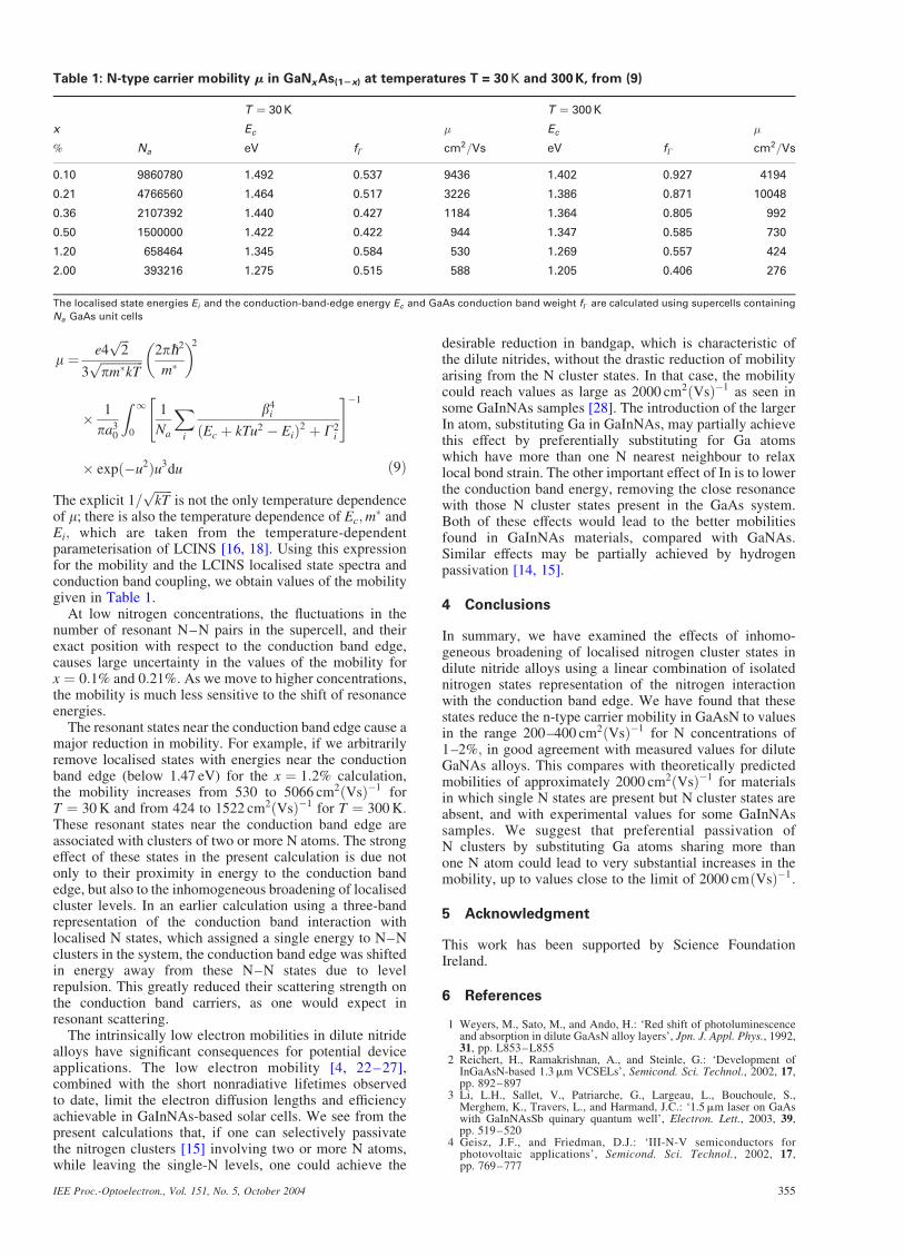
� andEi; which are taken from the temperature-dependentparameterisation of LCINS [16, 18]. Using this expressionfor the mobility and the LCINS localised state spectra andconduction band coupling, we obtain values of the mobilitygiven in Table 1.
At low nitrogen concentrations, the fluctuations in thenumber of resonant N–N pairs in the supercell, and theirexact position with respect to the conduction band edge,causes large uncertainty in the values of the mobility forx ¼ 0:1% and 0:21%: As we move to higher concentrations,the mobility is much less sensitive to the shift of resonanceenergies.
The resonant states near the conduction band edge cause amajor reduction in mobility. For example, if we arbitrarilyremove localised states with energies near the conductionband edge (below 1.47 eV) for the x ¼ 1:2% calculation,the mobility increases from 530 to 5066 cm2ðVsÞ�1 forT ¼ 30K and from 424 to 1522 cm2ðVsÞ�1 for T ¼ 300K:These resonant states near the conduction band edge areassociated with clusters of two or more N atoms. The strongeffect of these states in the present calculation is due notonly to their proximity in energy to the conduction bandedge, but also to the inhomogeneous broadening of localisedcluster levels. In an earlier calculation using a three-bandrepresentation of the conduction band interaction withlocalised N states, which assigned a single energy to N–Nclusters in the system, the conduction band edge was shiftedin energy away from these N–N states due to levelrepulsion. This greatly reduced their scattering strength onthe conduction band carriers, as one would expect inresonant scattering.
The intrinsically low electron mobilities in dilute nitridealloys have significant consequences for potential deviceapplications. The low electron mobility [4, 22–27],combined with the short nonradiative lifetimes observedto date, limit the electron diffusion lengths and efficiencyachievable in GaInNAs-based solar cells. We see from thepresent calculations that, if one can selectively passivatethe nitrogen clusters [15] involving two or more N atoms,while leaving the single-N levels, one could achieve the
desirable reduction in bandgap, which is characteristic ofthe dilute nitrides, without the drastic reduction of mobilityarising from the N cluster states. In that case, the mobilitycould reach values as large as 2000 cm2ðVsÞ�1 as seen insome GaInNAs samples [28]. The introduction of the largerIn atom, substituting Ga in GaInNAs, may partially achievethis effect by preferentially substituting for Ga atomswhich have more than one N nearest neighbour to relaxlocal bond strain. The other important effect of In is to lowerthe conduction band energy, removing the close resonancewith those N cluster states present in the GaAs system.Both of these effects would lead to the better mobilitiesfound in GaInNAs materials, compared with GaNAs.Similar effects may be partially achieved by hydrogenpassivation [14, 15].
4 Conclusions
In summary, we have examined the effects of inhomo-geneous broadening of localised nitrogen cluster states indilute nitride alloys using a linear combination of isolatednitrogen states representation of the nitrogen interactionwith the conduction band edge. We have found that thesestates reduce the n-type carrier mobility in GaAsN to valuesin the range 200–400 cm2ðVsÞ�1 for N concentrations of1–2%; in good agreement with measured values for diluteGaNAs alloys. This compares with theoretically predictedmobilities of approximately 2000 cm2ðVsÞ�1 for materialsin which single N states are present but N cluster states areabsent, and with experimental values for some GaInNAssamples. We suggest that preferential passivation ofN clusters by substituting Ga atoms sharing more thanone N atom could lead to very substantial increases in themobility, up to values close to the limit of 2000 cmðVsÞ�1:
5 Acknowledgment
This work has been supported by Science FoundationIreland.
6 References
1 Weyers, M., Sato, M., and Ando, H.: ‘Red shift of photoluminescenceand absorption in dilute GaAsN alloy layers’, Jpn. J. Appl. Phys., 1992,31, pp. L853–L855
2 Reichert, H., Ramakrishnan, A., and Steinle, G.: ‘Development ofInGaAsN-based 1.3mm VCSELs’, Semicond. Sci. Technol., 2002, 17,pp. 892–897
3 Li, L.H., Sallet, V., Patriarche, G., Largeau, L., Bouchoule, S.,Merghem, K., Travers, L., and Harmand, J.C.: ‘1.5mm laser on GaAswith GaInNAsSb quinary quantum well’, Electron. Lett., 2003, 39,pp. 519–520
4 Geisz, J.F., and Friedman, D.J.: ‘III-N-V semiconductors forphotovoltaic applications’, Semicond. Sci. Technol., 2002, 17,pp. 769–777
Table 1: N-type carrier mobility m in GaNx As(12x) at temperatures T = 30 K and 300 K, from (9)
T ¼ 30 K T ¼ 300 K
x Ec � Ec �
% Na eV fG cm2=Vs eV fG cm2=Vs
0.10 9860780 1.492 0.537 9436 1.402 0.927 4194
0.21 4766560 1.464 0.517 3226 1.386 0.871 10048
0.36 2107392 1.440 0.427 1184 1.364 0.805 992
0.50 1500000 1.422 0.422 944 1.347 0.585 730
1.20 658464 1.345 0.584 530 1.269 0.557 424
2.00 393216 1.275 0.515 588 1.205 0.406 276
The localised state energies Ei and the conduction-band-edge energy Ec and GaAs conduction band weight fG are calculated using supercells containing
Na GaAs unit cells
IEE Proc.-Optoelectron., Vol. 151, No. 5, October 2004 355
5 Shan, W., Walukiewicz, W., Ager, J.W., III, Haller, E.E., Geisz, J.F.,Friedman, D.J., Olson, J.M., and Kurtz, S.R.: ‘Band anticrossing inGaInNAs alloys’, Phys. Rev. Lett., 1999, 82, pp. 1221–1224
6 Kent, P.R.C., and Zunger, A.: ‘Theory of electronic structure evolutionin GaAsN and GaPN alloys’, Phys. Rev. B, Condens. Matter Mater.Phys., 2001, 64, art. no. 115208
7 Zhang, Y., Mascarenas, A., Geisz, J.F., Xin, H.P., and Tu, C.W.:‘Discrete and continuous spectrum of nitrogen-related bound states inheavily doped GaAsN’, Phys. Rev. B, Condens. Matter Mater. Phys.,2001, 63, p. 085205
8 O’Reilly, E.P., Lindsay, A., Tomic, S., and Kamal-Saadi, M.: ‘Tight-binding and k.p models for the electronic structure of Ga(In)NAs andrelated alloys’, Semicond. Sci. Technol., 2001, 17, pp. 870–879
9 Fahy, S., and O’Reilly, E.P.: ‘Intrinsic limits on electron mobility indilute nitride semiconductors’, Appl. Phys. Lett., 2003, 83,pp. 3731–3733
10 Fahy, S., and O’Reilly, E.P.: ‘Theory of electron mobility in dilutenitride semiconductors’, Physica E, 2004, 21, pp. 881–885
11 Hjalmarson, H.P., Vogl, P., Wolford, D.J., and Dow, J.D.: ‘Theory ofsubstitutional deep traps in covalent semiconductors’, Phys. Rev. Lett.,1980, 44, pp. 810–813
12 Liu, X., Pistol, M.-E., Samuelson, L., Schwetlick, S., and Siefert, W.:‘Nitrogen luminescence in GaAs’, Appl. Phys. Lett., 1990, 56,pp. 1451–1453
13 Polimeni, A., Hogersthal, Bissiri, G., Capizzi, M., Frova, A.,Fischer, M., Reinhardt, M., and Forchel, A.: ‘Role of hydrogen inIII-N-V compound semiconductors’, Semicond. Sci. Technol., 2002, 17,pp. 797–802
14 Polimeni, A., Bissiri, M., Felici, M., Capizzi, M., Buyanova, I.A.,Chen, W.M., Xin, H.P., and Tu, C.W.: ‘Nitrogen passivation induced byatomic hydrogen: the GaPN case’, Phys. Rev. B, Condens. MatterMater. Phys., 2003, 67, p. 201303(R)
15 Buyanova, I.A., Izadifard, M., Chen, W.M., Polimeni, A., Capizzi, M.,Xin, H.P., and Tu, C.W.: ‘Hydrogen-induced improvements in theoptical quality of GaNAs alloys’, Appl. Phys. Lett., 2003, 82,pp. 3662–3664
16 Lindsay, A., and O’Reilly, E.P.: ‘A tight-binding-based analysisof the band anti-crossing model in GaNAs’, Physica E, 2004, 21,pp. 901–906
17 Vogl, P.: ‘Predictions of deep impurity level energies in semiconduc-tors’, Adv. Electron. Electron Phys., 1984, 62, pp. 101–159
18 Lindsay, A., O’Reilly, E.P. and Fahy, S.: J. Phys., Condens. Matter,(to be published)
19 Gale, J.: ‘GULP – a computer program for the symmetry adaptedsimulation of solids’, J. Chem. Soc. Faraday Trans., 1997, 93,pp. 629–637
20 Lindsay, A., and O’Reilly, E.P.: (submitted to Phys. Rev. Lett.)21 Sankey, O.F., Dow, J.D., and Hess, K.: ‘Theory of resonant scattering in
semiconductors due to impurity central-cell potentials’, Appl. Phys.Lett., 1982, 41, pp. 664–666
22 Suemune, I., Uesugi, K., and Walukiewicz, W.: ‘Role of nitrogen in thereduced temperature dependence of band-gap energy in GaNAs’, Appl.Phys. Lett., 2000, 77, pp. 3021–3023
23 Hong, Y.G., Tu, C.W., and Ahrenkiel, R.K.: ‘Improving properties ofGaInNAs with a short-period GaNAs/GaInAs superlattice’, J. Cryst.Growth, 2001, 227–228, pp. 536–540
24 Geisz, J.F., Friedman, D.J., Olson, J.M., Kurtz, S.R., and Keyes, B.M.:‘Photocurrent of 1 eV GaInNAs lattice-matched to GaAs’, J. Cryst.Growth, 1998, 195, pp. 401–405
25 Kurtz, S.R., Allerman, A.A., Seager, C.H., Seig, R.M., and Jones, E.D.:‘Minority carrier diffusion, defects and localization in InGaAsN, with2% nitrogen’, Appl. Phys. Lett., 2000, 77, pp. 400–402
26 Li, W., Pessa, M., Toivonen, J., and Lipsanen, H.: ‘Doping and carriertransport in Ga123xIn3xNxAs12x alloys’, Phys. Rev. B, Condens. MatterMater. Phys., 2001, 64, art. no. 113308
27 Skierbiszweski, C.: ‘Experimental studies of conduction bandstructure of GaInNAs alloys’, Semicond. Sci. Technol., 2002, 17,pp. 803–814
28 Volz, K., Koch, J., Kunert, B., and Stolz, W.: ‘Doping behaviour of Si,Te, Zn and Mg in lattice-matched (GaIn)(NAs)/GaAs bulk films’,J. Cryst. Growth, 2003, 248, pp. 451–456
IEE Proc.-Optoelectron., Vol. 151, No. 5, October 2004356