Embed Size (px)
Citation preview

Intermetallics for Structural Applications in Micro Joints of 3D ICs
J. J. Yu, T. L. Yang, R. Y. Wu, and C. R. KaoDepartment of Materials Science and Engineering
National Taiwan University
1

TSV (Through Silicon Via) and Micro Joints as interconnection for 3D IC
3D IC integration provides a more direct and efficient way to integrate several heterogeneous functional components, such as Memory, Processor, Logic, Flash, and/or MEMS etc. in a package with the shortest distance.
3D IC integration
Source: http://www.3d‐ic.org/documents/IMIS_Press_Release.pdf
3D IC integration technology provides opportunities to go beyondMoore’s law.
2

Example of TSV‐3D IC Integration
Micron Hybrid Memory Cube Consortium
“combine a logic layer with several DRAM dies stacked atop” … “deliver 15 times the performance while utilizing 70% less energy.”
Source: The Micron HMC
Introduction
3

TSV and Micro‐joints as interconnection for 3D IC integration.
4

Volume ratio of IMC to solder increases dramatically!Intermetallic compounds dominate the properties of micro joints in 3D ICs.
Characterization of IMCs becomes an urgent issue..
BGA
Flip‐chip
3D IC micro joint
Significant Reduction of Solder Volume
5

Very small solder volume Solder will be transformed into intermetallic compounds completely during assembly or operation of a device.
Instead of solder, IMCs will dominate the mechanical property of the micro joints.
From regular solder joints to 3D IC micro‐joints: Extremely small solder volume !
Flip‐chip solder jointMicro joint
Solder
From flip‐chip joints to 3D‐IC micro joints, solder volume shrinks by a factor of 1000.
IMCSolder
Cu6Sn5
Cu6Sn5
6

Photo from M.D. Uchic, D.M. Dimiduk, Materials Science and Engineering: A 400–401 (2005) 268‐278.
FIB‐Assisted Testing Specimen Fabrication ‐Micropillar
• Milling a crater with a pillar located in thecenter.
• Using the same voltage and decreasing current,down to 0.2 nA.
• Refining the center pillar to a desired diameterand height.
dt
hθ
Geometry design:• Taper angle θ < 1.5° (to avoid overestimating
stress)• extremely small current is required.
• Aspect ration dt/h = 2‐3• dt/h < 2 : overestimating displacement. • dt/h > 3 : buckling.
7

Advantage of Micropillar Testing
43μm 2.3μm
4.6μm
90μm
1. Various sizes of pillars from 100μm to 100nm
Different sizes of Ni superalloy micropillars
[1] M.D. Uchic, D.M. Dimiduk, Materials Science and Engineering: A 400–401 (2005) 268‐278.[2] Z. Shan, JOM 64 (2012) 1229‐1234.[3] V. Sriram, J.‐M. Yang, J. Ye, A.M. Minor, Microelectronic Engineering 87 (2010) 2046‐2049.
[1]
Ni nanocrystalline sub‐micro pillar
[2]
Nanotwinned Cu sub‐micro pillar
500nm
[3]
8
2. Applicable to various materials 3. Various designs of structure
Al/SiC nanolaminates two pre‐tilt angles of ZrCu(metal glass)/Zr interface
[1] D. R .P. Singh, N. Chawla, G. Tang, Y.L. Shen, Acta Materialia 58 (2010) 6628‐6636.[2] J. Schwiedrzik, R. Raghavan, A. Burki, V. LeNader, U. Wolfram, J. Michler, P. Zysset, Nat Mater 13 (2014) 740‐747.[3] M.C. Liu, J.C. Huang, Y.T. Fong, S.P. Ju, X.H. Du, H.J. Pei, T.G. Nieh, Acta Materialia 61 (2013) 3304‐3313.
Dry ovine osteonal bone micropillar compression
4. Various mechanical properties• Yield strength• Fracture strength• Strain to failure• Interface strength• Failure mode• Slip system• Size effect
ZrCu
Zr
ZrCu
Si
[3]
[2]
[1]
Advantage of Micropillar Testing
9

Cu6Sn5 Micropillar Compression by Nanoindentation
6
• A Berkovich indenter with a flat triangular cross‐section (10μm on a side) was used.• Strain rate=0.05• The Sneddon equation was used to modify the punching effect of a cylindrical
punch indenting into an elastic half space.dp=displacement of pillardmeas=measured displacementEi/Eb=Young’s modulus of indenter/bulk=Poisson ratio
dt/db=diameter of top/bottom
L. Jiang, N. Chawla, Scripta Materialia 63 (2010) 480‐483.
1 1
Fracture strength:1356MPa
Strain to failure:1.37%
10

The results also show that there was a linear decrease in strength when the deviation angle to the c‐axisincreases.
There were a 7 % increase in Young’s modulus and 20% increase in strength along the c‐axis as compared with that normal to the c‐axis.
Effects of Cu6Sn5 Grain Orientation (Anisotropy)Crystallographic Orientation on the Mechanical Behavior of Cu6Sn5 by MicropillarCompression Testing L. Jiang, H. Jiang, and N. Chawla*, Journal of Electronic Materials, Vol. 41, No. 8, 2012.
Cu6Sn5
Cu3SnAg3Sn Cu
Cu
Is there any promising approach to control the orientation of Cu6Sn5 during bonding?
∥ to c‐axis ∥ to c‐axis
to c‐axis to c‐axis
∥ to c‐axis
to c‐axis
Sample jointed at 250 oC for 30s ITRI, Taiwan
900
c‐axis
∥ c‐axis
(degree)
11
Microstructure control of unidirectional growth of ‐Cu6Sn5 on <111> Nanotwinned‐Cu
H. W. Lin, C. L. Liu, C. M. Liu, C. Chen*, D. Chen, J. C. Kuo, K. N. Tu, Acta Materialia 61, 4910, 2013.
Sn-Ag(1) (2) (3) (4)
(5) (6) (7) (8)
ND
ND
The crystallographic orientation of Cu6Sn5 grains show a strong texture by using <111> Nanotwinned Cu.12

2. Applicable to various materials 3. Various designs of structure
Al/SiC nanolaminates two pre‐tilt angles of ZrCu(metal glass)/Zr interface
[1] D. R .P. Singh, N. Chawla, G. Tang, Y.L. Shen, Acta Materialia 58 (2010) 6628‐6636.[2] J. Schwiedrzik, R. Raghavan, A. Burki, V. LeNader, U. Wolfram, J. Michler, P. Zysset, Nat Mater 13 (2014) 740‐747.[3] M.C. Liu, J.C. Huang, Y.T. Fong, S.P. Ju, X.H. Du, H.J. Pei, T.G. Nieh, Acta Materialia 61 (2013) 3304‐3313.
Dry ovine osteonal bone micropillar compression
4. Various mechanical properties• Yield strength• Fracture strength• Strain to failure• Interface strength• Failure mode• Slip system• Size effect
ZrCu
Zr
ZrCu
Si
[3]
[2]
[1]
Advantage of Micropillar Testing
13
[2] Y. Takahashi, H. Kondo, H. Niimi, T. Nokuo, T. Suzuki, Sensors and Actuators A: Physical 206 (2014) 81‐87.
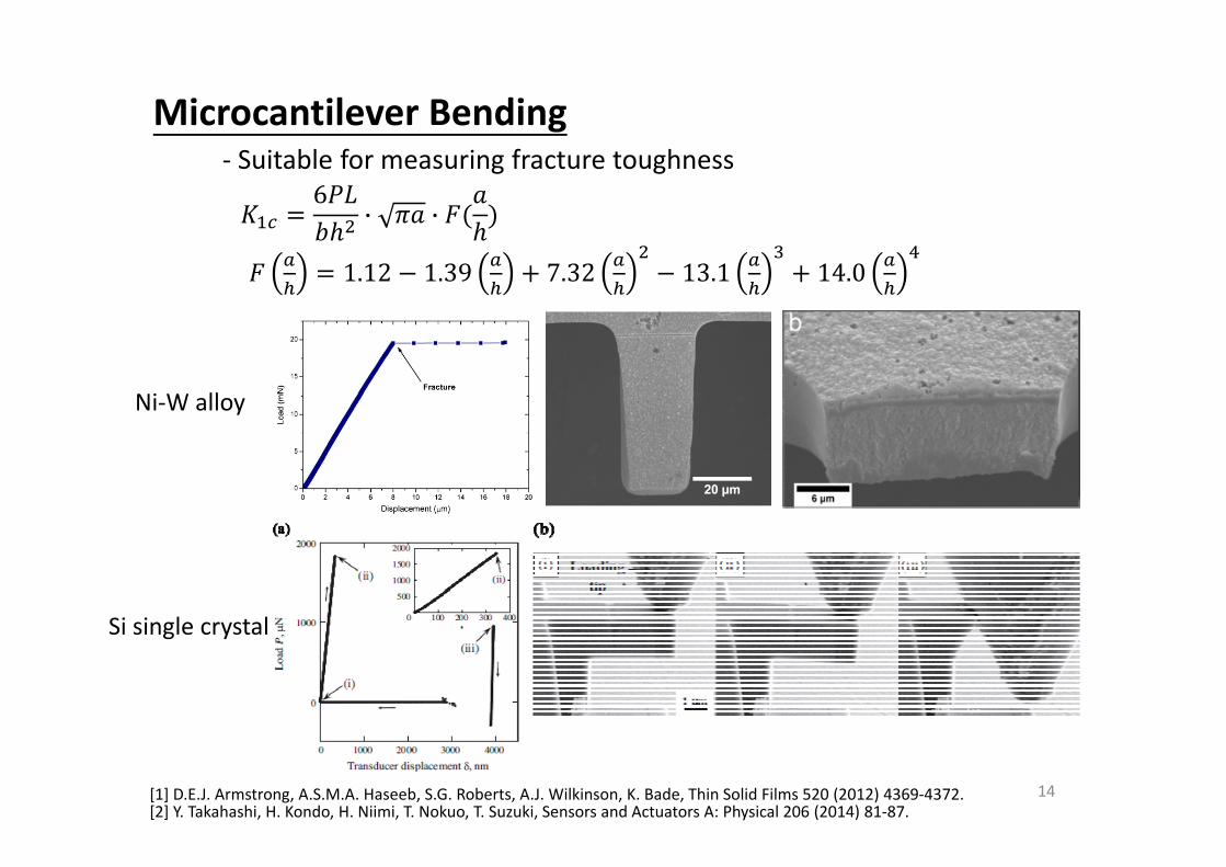
Microcantilever Bending‐ Suitable for measuring fracture toughness
[1] D.E.J. Armstrong, A.S.M.A. Haseeb, S.G. Roberts, A.J. Wilkinson, K. Bade, Thin Solid Films 520 (2012) 4369‐4372.
Ni‐W alloy
Si single crystal
6· ·
1.12 1.39 7.32 13.1 14.0
14

Picoindentation
1, lower part of the main frame2, supporting rib3, upper part of the main frame4, transducer in its support5, conductive indenter probe6, z slip‐stick actuator7, x, y slip‐stick actuators8, removable sample holder9, SEM stage10, SEM electron gun11, SEM high‐magnification detector.
Advantage:• Position the probe accurately and effectively.• Imaging the deformation process during the test.
K.A. Rzepiejewska‐Malyska et al., Journal of Materials Research 23 (2008) 1973‐1979. 15

Objectives of Our Works
• Using Picoindenter to• determine the mechanical properties of single crystalline
IMCs (Cu6Sn5, Ni3Sn4, Cu3Sn etc), polycrystalline IMCs, aswell as interfaces between metals and IMCs by micropillar compression.
• determine the fracture toughness of IMCs and grainboundaries of IMCs by cantilever bending.
16

0.127 mm Cu disk
Sn foil/granule
Reflow250℃,1min
+Heat Treatment300℃,168h
Mounting& Polishing
Top view
Cross‐section
40μm 40μm
Interfacial Reaction
Micropillarfabrication by FIB
CuCu3Sn
Cu6Sn5
Sn
50μm 10μm
Sample Preparation ‐ Interfacial Reaction
EBSD
EBSD
Acquiring grain
orientation
Acquiring grain
orientation
17

Stoichiometric Cu slug & Sn drop were added into a tube
Melting In sealed tube under
vacuum800°C,7 days
4N Sn drop5N Cu slug
Cu6Sn5 disc was cut from bulk ingot
Sample Preparation ‐ Alloying
Polishing
Micropillarfabrication by FIB
380°C for η phase180°C for η’ phase
Homogenization
η’η
EBSD
Acquiring grain
orientation
18

19
Chawla’sIn this study
Top diameter≈2.4Length≈7.5 Aspect ratio≈3Taper angle<2 °
Top diameter=2~3Length=5~8Aspect ratio=2~2.5Taper angle=1~1.5°
Micropillar Fabrication
19

Obtaining Stress‐Strain Curve
Load‐displacement curve(raw) Stress‐strain curve(modified)
1 1 Considering the punching effect ofa cylindrical punch indenting intoan elastic half‐space
Converting displacement into strain
Converting load into stress
20

Micropillar Compression
Strain rate:1x10‐3
Strain rate:2x10‐4
Cleavage plane
Cleavage plane
Split along same crystallographic plane.
21

Strain rate: 5x10‐2s‐1
Strain rate: 1x10‐3s‐1
Strain rate: 2x10‐4s‐1
Compared to Reference
L. Jiang, H. Jiang, and N. Chawla, Journal of Electronic Materials, Vol41, No.8 ,2012
Strainrate s‐1 5x10‐2 1x10‐3 2x10‐4
Fracture strength MPa 1724 242 1289 1252.02
Straintofailure 0.012 0.001 0.020 0.023
Engineering Strain
Engine
ering Stress(M
Pa)
220020001800
⊥ c‐axis
// c‐axis
02004006008001000120014001600
0 0.005 0.01 0.015 0.02 0.025 0.03
22

• Adding Ni to Cu6Sn5 to investigate the effect of Niconcentration on various mechanical properties of(Cu,Ni)6Sn5
• To study the difference of mechanical properties betweenη’‐Cu6Sn5 and η‐Cu6Sn5.
• To fabricate multilayer structure to simulate themechanical properties of real 3D IC micro joints in variousstages of IMC growth.
• To collect mechanical property data that are essential forindustrial reliability modeling.
Future works
23


![Color Panel Memory Test [CPMT]](https://img.pdfslide.us/doc/110x75/549ab475b4795938098b4593/color-panel-memory-test-cpmt.jpg)