Embed Size (px)
Citation preview

AN1278Interleaved Power Factor Correction (IPFC)
Using the dsPIC® DSC
INTRODUCTION
Digital power supplies are used in a wide variety ofapplications ranging from telecommunication powersupplies and base stations to air conditioners and otherhome appliances. All of these applications predomi-nantly use a Power Factor Correction (PFC) stage toimprove the input power factor, voltage regulation andTotal Harmonic Distortion (THD) of the input current.Without such a PFC stage, the current drawn will havesignificant harmonic contents due to the discontinuouscurrents drawn over a short duration. This, in turn, willresult in increased network losses, radiated emissionand total harmonic distortion. At higher power levels,these problems become more pronounced, therebyreducing overall efficiency of the system.
The standard boost converter topology is the preferredmethod for implementing the digital PFC. It operates theconverter in Continuous Conduction Mode (CCM),thereby significantly reducing input current harmonics.The application note AN1106, “Power Factor Correctionin Power Conversion Applications Using the dsPIC®
DSC” (DS01106), describes the digital implementation ofa single-stage PFC using a dsPIC® Digital SignalController (DSC).
This application note focuses on the design of anInterleaved Power Factor Correction (IPFC) converter.It explains the digital implementation of the IPFC on a16-bit fixed point dsPIC DSC, containing the theoreticalaspects of functioning, and MATLAB® modeling. Thisapplication note also provides hardware designguidelines and explains how to install and configure theIPFC reference board. The IPFC reference design isintended to aid the user in the rapid evaluation anddevelopment of PFC using the dsPIC DSC.
The low-cost and high-performance capabilities of thedsPIC DSC, combined with a wide variety of powerelectronic peripherals, such as an Analog-to-DigitalConverter (ADC), Pulse-Width Modulator (PWM) andAnalog Comparator, help to simplify the digital designand development of power-related applications.
Some advantages of using a digital implementation forIPFC are:
• Easy implementation of sophisticated control algorithms
• Flexible software modifications to meet specific customer needs
• Simpler integration with other applications
The controller and hardware design guidelines andtechniques described here can be used to create well-formed maintainable applications. The softwaredeveloped for the IPFC design is highly flexible, so itcan be customized and configured to meet the needsof the specific application.
SIGNIFICANCE OF POWER FACTOR
To better understand Power Factor (PF), it is importantto know that power has two components:
• Real Power
• Reactive Power
Real Power is the power that is actually consumed andregistered on the electric meter at the consumers’ loca-tion. It performs the actual work, such as creating heat,light and motion. Real Power is expressed in kW and isregistered as kWH on an electric meter.
Reactive Power is required to maintain and sustain theElectromagnetic Field (EMF) associated with theindustrial inductive loads. Reactive Power is measuredin kVAR.
The total required power capacity including the real andthe reactive components is known as Apparent Power,expressed in kilovolt ampere (kVA).
Power Factor is a parameter that gives the amount ofreal power used by any system in terms of the totalapparent power. Power Factor becomes an importantmeasurable quantity because it often results in signifi-cant economic savings. Equation 1 defines the PowerFactor.
EQUATION 1:
Authors: Vinaya Skanda and Anusheel Nahar Microchip Technology Inc.
Power FactorReal Power
Apparent Power---------------------------------------=
2009 Microchip Technology Inc. DS01278A-page 1

AN1278
When this ratio deviates from one, the input containsphase displacement and harmonic distortion or both,and either one degrades the Power Factor. Thus, thepower considered as Reactive power in the system isdue to two reasons:
• Phase shift of current with respect to voltage, resulting in displacement
• Harmonic content present in current, resulting in distortion
These two factors define Displacement Factor andDistortion Factor, respectively, which provide thePower Factor as shown in Equation 2.
Most power conversion applications use the PFC stageas the first stage in an AC-to-DC converter to improvethe displacement and distortion factors so thatminimum Apparent Power can be obtained from thesupply. To reduce the losses in a power line and apower generator, minimum apparent power isabsorbed from the supply, resulting in the improvementof power quality and overall efficiency of the system.The basic function of the PFC stage is to make theinput current drawn from the system sinusoidal and inphase with the input voltage.
EQUATION 2: DISPLACEMENT AND DISTORTION FACTOR
Power Factor = Displacement Factor x Distortion Factor
where:
cos Displacement factor of the voltage and current
THD = Total Harmonic Distortion
I1 = Current drawn from the supply at fundamental frequency
I2 = Current drawn from the supply at double the fundamental frequency and so on
PowerFactor cos1
1 I2 I1 2 I3 I1 2 + + +--------------------------------------------------------------------- cos
1 THD2+
----------------------------= =
DisplacementFactor Distortion Factor
THD I2 I1 2 I3 I1 2 + +=
DS01278A-page 2 2009 Microchip Technology Inc.
AN1278
TOPOLOGICAL CONSIDERATIONS OF TWO-PHASE IPFC
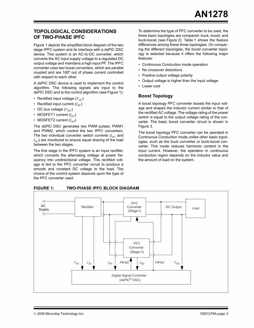
Figure 1 depicts the simplified block diagram of the twostage IPFC system and its interface with a dsPIC DSCdevice. This system is an AC-to-DC converter, whichconverts the AC input supply voltage to a regulated DCoutput voltage and maintains a high input PF. The IPFCconverter uses two boost converters, which are parallelcoupled and are 180º out of phase current controlledwith respect to each other.
A dsPIC DSC device is used to implement the controlalgorithm. The following signals are input to thedsPIC DSC and to the control algorithm (see Figure 1):
• Rectified input voltage (VAC)
• Rectified input current (IAC)
• DC bus voltage (VDC)
• MOSFET1 current (Im1)
• MOSFET2 current (Im2)
The dsPIC DSC generates two PWM pulses: PWM1and PWM2, which control the two IPFC converters.The two individual converter switch currents (Im1 andIm2) are monitored to ensure equal sharing of the loadbetween the two stages.
The first stage in the IPFC system is an input rectifier,which converts the alternating voltage at power fre-quency into unidirectional voltage. This rectified volt-age is fed to the PFC converter circuit to produce asmooth and constant DC voltage to the load. Thechoice of the control system depends upon the type ofthe PFC converter used.
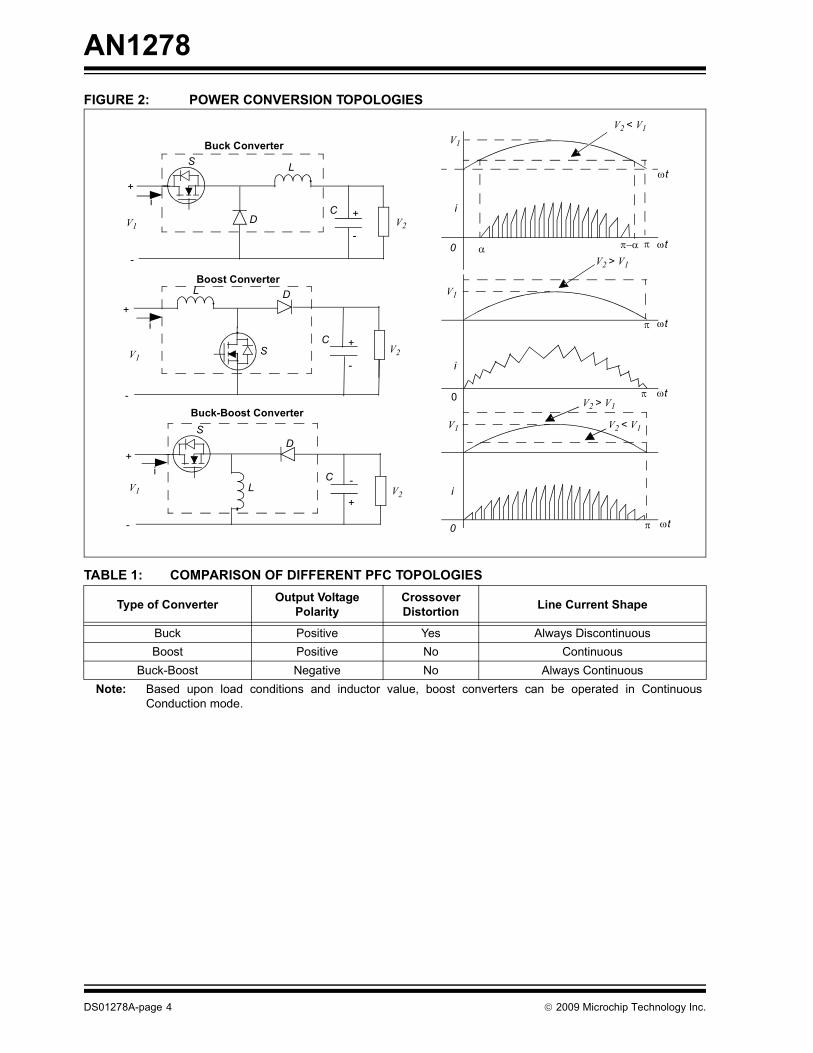
To determine the type of PFC converter to be used, thethree basic topologies are compared: buck, boost, andbuck-boost (see Figure 2). Table 1 shows the featuredifferences among these three topologies. On compar-ing the different topologies, the boost converter topol-ogy is selected because it offers the following majorfeatures:
• Continuous Conduction mode operation
• No crossover distortions
• Positive output voltage polarity
• Output voltage is higher than the input voltage
• Lower cost
Boost Topology
A boost topology PFC converter boosts the input volt-age and shapes the inductor current similar to that ofthe rectified AC voltage. The voltage rating of the powerswitch is equal to the output voltage rating of the con-verter. The basic boost converter circuit is shown inFigure 3.
The boost topology PFC converter can be operated inContinuous Conduction mode unlike other basic topol-ogies, such as the buck converter or buck-boost con-verter. This mode reduces harmonic content in theinput current. However, the operation in continuousconduction region depends on the inductor value andthe amount of load on the system.
FIGURE 1: TWO-PHASE IPFC BLOCK DIAGRAM
Rectifier
Digital Signal Controller(dsPIC® DSC)
Load
VAC IAC VDC
PFC Converter
(Stage I)
PFC Converter(Stage II)
IM1 IM2
DC Output
PWM2 PWM1
ACSupply
2009 Microchip Technology Inc. DS01278A-page 3
AN1278
FIGURE 2: POWER CONVERSION TOPOLOGIES
Buck Converter
Boost Converter
Buck-Boost Converter
V1
S
D
L
C
-
+
+
-
i
V2
S
DL
C
-
+
+
-
i
V2
SD
LC
-
+
-
+
i
V2
V1
V1
V1
i
i
i
0
0
0
t
t
t
t
t
V1
V1
V2 < V1
V2 > V1
V2 > V1
V2 < V1
TABLE 1: COMPARISON OF DIFFERENT PFC TOPOLOGIES
Type of ConverterOutput Voltage
PolarityCrossover Distortion
Line Current Shape
Buck Positive Yes Always Discontinuous
Boost Positive No Continuous
Buck-Boost Negative No Always Continuous
Note: Based upon load conditions and inductor value, boost converters can be operated in ContinuousConduction mode.
DS01278A-page 4 2009 Microchip Technology Inc.

AN1278
IPFC DIGITAL DESIGN
In general, the PFC offers the following advantages:
• Lower energy and distribution costs
• Reduced losses in the electrical system during distribution
• Better voltage regulation
• Increased capacity to serve power requirements
The following are the limitations of a single-stage PFCwhen compared to an IPFC converter:
• Current ripple cancellation is not possible
• Unequal sharing of load when two converters are in parallel
• Large PFC inductor volume
The IPFC converter can overcome these limitations. Itcontains two boost converters, which are parallel cou-pled and are 180º out of phase current controlled withrespect to each other, as shown in Figure 3.
At the input side, the total input current (IAC) drawn fromthe source equals the sum of the two inductor currents(IL1 and IL2). Because the ripple currents through thetwo inductors are out of phase, they cancel each otherand reduce the total ripple current in the input side. Ata duty cycle of 50%, the best cancellation of ripplecurrents is possible.
At the output side, current through the output capacitor(IC) equals the sum of the two diode currents (ID1 andID2) minus the output current (ILOAD).
FIGURE 3: IPFC BOOST CONVERTER CIRCUIT
Rectifier
PWM1H IM1
PWM1L
IL2
IM2
ID2 PFC
C
Lo
ad
ADC PWM
Output
ADC ADC ADC ADC
dsPIC® DSC
IL1 ID1 ILoad
IC
2009 Microchip Technology Inc. DS01278A-page 5

AN1278
FIGURE 4: IPFC SIGNALS
PWM1H
PWM1L
IL1
IL2
ID1
ID2
IC = (ID1 + ID2) - 1
t
t
t
t
t
t
t
DS01278A-page 6 2009 Microchip Technology Inc.

AN1278
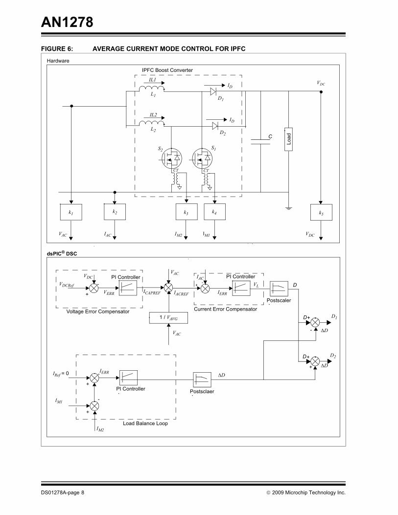
Average Current Mode Control
The IPFC system uses the average current mode con-trol method to meet the system requirements. The IPFCsystem uses the average current mode control methodto meet the system requirements. For PFC, this controlmethod is used to regulate DC output voltage whilekeeping the input current shape sinusoidal and in phasewith the input voltage.
The control method operates in Continuous Conductionmode in most parts of the operating regions of theconverter. The operation is primarily based on the valueof the load current at any point and the selection of theinductor.
The various advantages offered by the AverageCurrent Mode Control over other methods include:
• Suitable for operation at higher power levels
• Less ripple current in the inductors
• Reduces EMI filter requirements
• Less RMS current will be drawn from the power supply
• Continuous Conduction mode operation is possible
To derive the sine shape for the average inductorcurrent, either a sinusoidal pattern can be generated insoftware or the rectified voltage itself can be used as areference. Here, the rectified voltage is used to get thenecessary shape of inductor current. TS is the totalPWM switching period, tON is the MOSFET conductiontime, and tOFF is the time during which the MOSFET isturned off. The control system controls the tON time inorder to derive the necessary shape of the inductorcurrent (see Figure 5). Figure 6 shows the blockdiagram of the digital average current mode controlscheme.
FIGURE 5: IPFC INPUT CURRENT WAVEFORM
IL
Average Inductor VAC /L
tON tOFF
T
(VAC VDC ) / L
PWM Switching Cycle Line Half Cycle
-
ILCurrent is controlled
2009 Microchip Technology Inc. DS01278A-page 7
AN1278
FIGURE 6: AVERAGE CURRENT MODE CONTROL FOR IPFC
k1
Lo
ad
k2 k5
VAC
C
D1
VDC
+
-
VERR
IAC
IERR
Current Error Compensator
IACREFICAPREF
VAC
*VDCRef
1 / VAVG
IPFC Boost Converter
dsPIC® DSC
IDVDC
L1
D2
ID
L2
S2
+
-IERRIRef = 0
+
-IM1
k3 k4
+- VL
D1
D2
D
D
D
D
Load Balance LoopIM2
IM2 IM1IAC VDC
Hardware
Voltage Error Compensator
PI Controller
PI Controller PI Controller
+
+
+
-
VAC
Postsclaer
D
Postscaler
D
S1
IL1
IL2
CT CT
DS01278A-page 8 2009 Microchip Technology Inc.

AN1278
Control Loops
The IPFC control system includes the following controlloops:
• Voltage Control Loop
• Current Control Loop
• Load Balance Control Loop
• Input and Output Voltage Decoupling Loop
VOLTAGE CONTROL LOOP
This is a PI controller and the outermost loop in thecontrol system. This loop regulates the output voltageregardless of any variations in load current (ILoad) andthe supply voltage (VAC). These are the inputs to thevoltage control loop:
• Reference DC voltage (VDCREF)
• DC bus voltage (VDC)
The output of the voltage control loop is a controlsignal, which determines the reference current (IACREF)for the current control loop.
The voltage control loop executes at a rate of 2 kHz andthe bandwidth of the voltage control loop is 10 Hz. Thebandwidth is selected such that the effect of the inputfrequency ripple on the output DC voltage can beminimized at 100 Hz or 120 Hz.
CURRENT CONTROL LOOP
This is a PI controller and the inner loop of the controlsystem. This loop corrects the error between these twocurrents, which are the inputs to the current controlloop:
• Reference current signal (IACREF)
• Input current (IAC)
The output of the current control loop is a control signal,which ensures that the input current (IAC) follows thereference current (IACREF).
The current control loop executes at a rate of 50 kHzand its bandwidth is 4 kHz for a switching frequency of100 kHz. The current control loop bandwidth and theexecution rate should be much faster than that of thevoltage control loop because it has to correctly trackthe semisinusoidal waveform whose frequency is twicethe input frequency. The output of the current controlloop decides the duty cycle ‘D’ required to switch theMOSFETs.
LOAD BALANCE CONTROL LOOP
The individual output voltage of each boost convertermay differ by a small value. This drift is possiblebecause of differences in the internal characteristics ofthe MOSFETs, internal resistances of the inductors,capacitors and the diodes. Therefore, when the sameduty cycle is applied to both the MOSFETs, it mayresult in unequal sharing of the load between the twoboost converter stages. This necessitates the presenceof a load balance control loop that balances the cur-rents in the two boost converter switches, which in turnresults in the equal sharing of load between the twoconverters.
One of the inputs to the load balance control loop isthe difference between the two MOSFET currents(IM1- IM2) of the two boost converters. The other input,which acts as a reference to this control loop, is tied tozero. This control loop mainly corrects the differencebetween the MOSFET currents and brings it close tothe reference input, which is zero. The output of theload balance control loop will be a duty correctionterm (D), which is added to the main duty cycle ‘D’ toget the duty cycle of the first boost converter, D1. TheD term is subtracted from the main duty cycle ‘D’ todetermine the duty cycle of the second boostconverter, D2.
INPUT AND OUTPUT VOLTAGE DECOUPLING LOOP
The IPFC also regulates the output DC voltage regard-less of variations in the input voltage. This is achievedby decoupling the system from the input voltage. Theoutput of the current error compensator derives thefinal duty cycle value of the MOSFETs. It considers thevariations in the VAC signal.
2009 Microchip Technology Inc. DS01278A-page 9

AN1278
Digital Design of IPFC
In a dsPIC DSC-based application, the relevant analogparameters are discretized. This enables for easier anda more logical changeover from existing hardware to itsdigital counterpart. Table 2 shows the various hardwareand software design parameters for the IPFC con-verter.
TABLE 2: HARDWARE AND SOFTWARE DESIGN PARAMETERS
DESIGN OF COMPENSATORS
All the compensators use digitally implementedProportional-Integral (PI) controllers. The followingsections describe the process used to select the pro-portional and integral gains for the voltage, current andload balance compensators.
Using the design parameters defined in Table 2, thefollowing parameters are calculated (see Equation 3):
• Maximum resistance
• Maximum conductance
EQUATION 3:
No. Design Parameter Symbol Value
Hardware Parameters
1 Output power Pout 350 watt
2 Input voltage range (rms) Vin 85V to 265V
3 Input frequency range f 45 Hz to 66 Hz
4 Output voltage VDC 400V
5 Output capacitance C 360 F
6 Inductance L1, L2 700 H
7 Switching frequency fs 100 kHz
Software Parameters
1 Voltage control loop frequency fVLoop 2 kHz
2 Current control loop frequency fILoop 50 kHz
3 Load balance control loop frequency fLBLoop 2 kHz
4 Voltage feedforward loop frequency fFFLoop 50 kHz
5 Average voltage calculation frequency fAVG 100 kHz
6 Voltage loop bandwidth BWVLoop 10 Hz
7 Current loop bandwidth BWILoop 4 kHz
8 Integral voltage loop bandwidth IBWVLoop 2.5 Hz
9 Integral current loop bandwidth IBWILoop 1 kHz
10 Load balance loop bandwidth BWLBLoop 200 Hz
Rmax
Vmax
Imax------------=
max1
Rmax------------=
Rmax440V
12.54A----------------- 35.08==
max1
35.08------------------ 0.0285 mho==
where:
Rmax = Maximum resistance
max = Maximum conductance
DS01278A-page 10 2009 Microchip Technology Inc.

AN1278
VOLTAGE ERROR COMPENSATOR
In the voltage error compensator, the input is thedifference in voltages and the output is the capacitorcurrent; therefore, the transfer function has a unit ofconductance. The transfer function is divided by themaximum conductance (or multiplied by the maximumresistance) in order to get the output in the range of -1to +1, similar to per unit quantities.
The proportional gain for the voltage error compensatoris derived using the small signal model of the boostconverter (see Equation 4).
EQUATION 4:
CURRENT ERROR COMPENSATOR
In the current error compensator, the input is thedifference in currents and the output is the inductor volt-age and therefore, the transfer function has a unit ofresistance. This quantity is divided by a factor of maxi-mum resistance (or multiplied by a factor of maximumconductance) to get the output in the range of -1 to +1.
The Proportional Gain for the current errorcompensator is derived using the small signal model ofthe boost converter (see Equation 5).
EQUATION 5:
LOAD BALANCE ERROR COMPENSATOR
Similar to the current error compensator, the load bal-ance compensator is also designed by normalizing theoutput to a range of -1 to +1.
The proportional gain for the load balancecompensator is derived using the small signal model ofthe boost converter (see Equation 6).
EQUATION 6:
AVERAGE VOLTAGE CALCULATION
The average value of the rectified input voltage is usedto derive the necessary shape of the sine wave. Inorder to get the half sinusoidal wave shape (i.e., theabsolute value of the sine) for the input current, theoutput of the voltage error compensator is multipliedwith a factor of |sin|. The resulting value acts as areference term to the input of the current errorcompensator. The |sin| can be obtained either by cre-ating a lookup table in software or can be extractedfrom the inherent shape of VAC, feedback of the rectifiedAC voltage, which will have the sinusoidal shape.
In this application, the sine wave shape is obtainedusing the feedback voltage VAC. The instantaneousinput rectified voltage VAC is given by Equation 7.
EQUATION 7:
To get the shape of the waveform, regardless of themagnitude of the input voltage, Equation 8 calculatesthe value of |sin|.
EQUATION 8:
Ga 2 C BWVLoop Rmax=
Gsa
2 Ga IBWVLoopfVLoop
---------------------------------------------------------=
where:
Ga = Proportional Gain for Voltage Error Compensator
Gsa = Integral Gain for Voltage Error Compensator
BWVLoop = Voltage Loop Bandwidth
IBWVLoop = Integral Voltage Loop Bandwidth
fVLoop = Voltage Control Loop Frequency
Ra 2 L BWILoop max=
Rsa
2 Ra IBWILoopfILoop
-------------------------------------------------------=
where:
Ra = Proportional Gain for Current Error Compensator
Rsa = Integral Gain for Current Error Compensator
BWILoop = Current Loop Bandwidth
IBWILoop = Integral Current Loop Bandwidth
fILoop = Current Control Loop Frequency
Ka 2 L BWLBLoop max=
Ksa
2 Ka IBWLBLoopfLBLoop
------------------------------------------------------------=
where:
Ka = Proportional Gain for Load Balance Error Compensator
Ksa = Integral Gain for Load Balance Error Compensator
BWLBLoop = Load Balance Loop Bandwidth
IBWLBLoop = Integral Load Balance Loop Bandwidth
fLBLoop = Load Balance Control Loop Frequency
VAC Vm Sin=
where:
Vm = Peak Voltage of the half sine wave
VAC = Rectified AC voltage
sinVACV
M
------------=
2009 Microchip Technology Inc. DS01278A-page 11

AN1278
For a full wave bridge rectifier output voltage, the peakvoltage can be expressed in terms of the averagevoltage (see Equation 9).
EQUATION 9:
Equation 10 is obtained by replacing the value of Vm inEquation 8. It ensures that the current reference term ismultiplied by only the half of the sine wave shape andremains unaffected by the magnitude of the voltage.
EQUATION 10:
Since the average value of the input voltage does notvary widely, the average voltage can be calculated andupdated once in many cycles.
INPUT AND OUTPUT VOLTAGE DECOUPLING CALCULATION
In the boost converter circuit, VDC is assumed to beclose to the base voltage (i.e., 400V). The followingequations are derived using Kirchhoff's laws (seeEquation 11).
EQUATION 11:
Thus, it is evident that the effect of input voltagevariations is compensated by correcting the main dutycycle (D), which is input to the load balance controlloop. The load balance compensator is used tocompute load correction term. Using the duty cycle (D)and load correction term, the individual duty cycles forthe two boost converters are derived.
Equation 12 describes the final equations that resultfrom the decoupling control loop.
EQUATION 12:
Performance Improvement by Interleaving Two PFCs
The inductor value is chosen depending on theallowable ripple current in the system. In a single stagePFC converter, for a given power level and theswitching frequency, the energy stored in the inductoris calculated using Equation 13. The amount of ripplecurrent, I, determines the value of the inductance ‘L’.
EQUATION 13:
In a two stage IPFC converter, for the same power leveland switching frequency, the energy stored in theinductors is computed using Equation 14.
EQUATION 14:
Here, the inductance for each stage is 2L, because theripple current in each stage is half of that of the singlestage PFC converter. Because of the interleaving, theripples tend to cancel out and a better performance forthe same component size is obtained. This also resultsin the lesser total line ripple current. Therefore, theripple current requirement of the individual stages arereduced, which in turn, reduces the inductancerequired for each of the stages.
Vavg
2Vm
----------=
Vm
Vavg2
---------------=
sin
2VACVavg------------------=
VAC VL– Dd VDC – 0=
Dd VAC VL– VDC=
D 1 Dd– 1 VAC VL– VDC–= =
where:
VAC = Input Rectified Voltage obtained from the ADC
VL = Inductor Voltage obtained from the current errorcompensator
VDC = Output DC Voltage obtained from ADC
D = Main Duty cycle
Dd = Duty cycle of a diode
D1 D D+=
D 1VAC VL–
VDC--------------------------–=
D2 D D–=
where:
D = Main duty cycle (D)
D1 = Duty cycle of MOSFET 1 (D1)
D2 = Duty cycle of MOSFET 2 (D2)
ESinglestage12---LI
2=
EInterleaved12--- 2L I
2--- 2 1
2--- 2L I2--- 2
+=
DS01278A-page 12 2009 Microchip Technology Inc.

AN1278
The ripple current (I) is chosen such that it is twice thatof the selected value. Therefore, the energy stored inthe inductors is computed using Equation 15.
EQUATION 15:
Function Usage in Software
All the functions used in this application software aredeveloped using the C language. The numerical con-stants and variables are defined in Q15 format or 1.15format. Because the selected dsPIC DSC device is a16-bit digital signal controller, if the gains or constantsexceed the range of 16 bits in the intermediate calcula-tions, they are appropriately prescaled to a different for-mat during computation and the end result is againconverted to the Q15 format by postscaling them.
Table 3 lists and describes the functions used in thesoftware (see Appendix A: “Source Code” foradditional information).
Note: For a given ripple content on the AC linecurrent, the inductor size can be reducedsignificantly by interleaving two boostconverters. Conversely, for a giveninductor size, the ripple currents can bereduced significantly (see Equation 15).
EInterleaved12--- L I
2--- 2 1
2--- L I2--- 2
+ 12---E
Singlestage= =
TABLE 3: FUNCTION USAGE IN SOFTWARE
File Name Function Name Description
Source Files
main.c main() Configures the operating frequency of the device.
Configures the auxiliary clock module.
Calls the functions for configuring ADC and PWM modules.
Checks the fault status.
adc_isr.c ADCP2Interrupt() Read values of currents and voltages.
Checks the fault condition.
Executes the various control loops, if fault doesn't exist.
Disables PWM outputs, if fault exists.
InitdsPIC.c Init_ADC() Configures the ADC module.
Init_PWM() Configure the PWM module.
Init_IO() Configures IO ports.
Init_CMP() Configures Analog Comparator module.
Vars.c — Declaration and Initialization of all the global variables.
compensators.c VoltageController() Executes the PI compensator for the voltage error compensator.
CurrentController() Executes the PI compensator for the current error compensator.
FeedForward() Provides the feedforward term and final duty cycle value.
AverageVoltageCalc() Calculates the average value of AC rectified voltage.
LoadBalance() Executes the load balance compensator for the two boost converters.
Header Files
defines.h(1) — Defines all the global function prototype and global parameters.
vars.h — Includes the supporting file for Vars.c .
Defines all the extern global definitions.
Note 1: This file is updated based on the type of hardware components used, power level, control loop frequencies,control loop bandwidth and other parameters. After these parameters are entered as per the design, theremaining gains are automatically calculated and scaled by the software. For further details, refer toAppendix A: “Source Code”.
2009 Microchip Technology Inc. DS01278A-page 13
AN1278
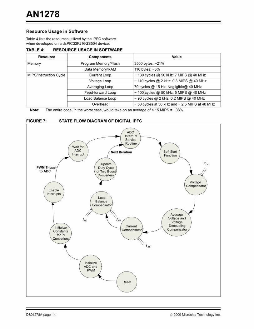
Resource Usage in Software
Table 4 lists the resources utilized by the IPFC softwarewhen developed on a dsPIC33FJ16GS504 device.
FIGURE 7: STATE FLOW DIAGRAM OF DIGITAL IPFC
TABLE 4: RESOURCE USAGE IN SOFTWARE
Resource Components Value
Memory Program Memory/Flash 3500 bytes: ~21%
Data Memory/RAM 110 bytes: ~5%
MIPS/Instruction Cycle Current Loop ~ 130 cycles @ 50 kHz: 7 MIPS @ 40 MHz
Voltage Loop ~ 110 cycles @ 2 kHz: 0.3 MIPS @ 40 MHz
Averaging Loop 70 cycles @ 15 Hz: Negligible@ 40 MHz
Feed-forward Loop ~ 100 cycles @ 50 kHz: 5 MIPS @ 40 MHz
Load Balance Loop ~ 90 cycles @ 2 kHz: 0.2 MIPS @ 40 MHz
Overhead ~ 50 cycles at 50 kHz and ~ 2.5 MIPS at 40 MHz
Note: The entire code, in the worst case, would take on an average of < 15 MIPS = ~38%
Reset
Initialize ADC and
PWM
InitializeConstants
for PIControllers
EnableInterrupts
Wait forADC
Interrupt
ADC InterruptService Routine
Soft StartFunction
VoltageCompensator
Average Voltage and
VoltageDecoupling
Compensator
LoadBalance
Compensator
UpdateDuty Cycle
of Two BoostConverters
Current Compensator
PWM Triggerto ADC
Next Iteration
VDC
IAC
IM1IM2
DS01278A-page 14 2009 Microchip Technology Inc.

AN1278
MATLAB® MODELING
The control system design for the IPFC system isaccomplished using the MATLAB SIMULINK® model.The various system gains and the parameter values ofthe PI controllers and the compensators are derivedusing this model. This section describes the MATLABmodeling, design considerations for the IPFC systemand the design constraints.
Figure 8 shows the IPFC MATLAB model and Figure 9shows the Digital Control System. Equation 16 listsanalytical expressions that describes the boostconverter circuit.
EQUATION 16: BOOST CONVERTER
The IPFC circuit performs the following major tasks:
1. Ensures that the input current follows the inputsupply voltage and assumes the same waveshape as that of the voltage (Distortion Factor).
2. Makes the input current drawn from the systemsinusoidal and in phase with the input voltage(Displacement Factor).
3. Maintains boost output voltage at a constant value(usually 400V) under varying load conditions andinput voltage. Typically, sine wave input voltage tothe rectifier varies from 85V to 265V rms.
The main objective of the control system is to controlthe inductor current (IAC) in order to track the referencesignal (IACREF) (see Figure 6). This reference signal isin phase with the rectified voltage and therefore, itchanges with time.
Typically, the rectified sine voltage has a frequency of100-120 Hz and it contains higher order harmonics.The reference current signal (IACREF) will also have thesame frequency. Therefore, for reliable commandtracking, the bandwidth required for current should beat least 10 times the frequency of IACREF signal.
For a switching frequency of ~100 kHz, the control loopbandwidth for current is chosen between 4000 Hz and6000 Hz. The voltage loop bandwidth is chosen to be10 Hz so that the current signal (100 or 120 Hz) doesnot get distorted. The zero bandwidth or Integral Volt-age Bandwidth selected here is one-fifth to one-fourthof the voltage loop bandwidth.
Because the voltage and current loop bandwidths arefar apart, they do not affect each other and are dis-jointed. So, approximate relations obtained from thecharacteristic equations are very near to the actualequations.
The following are the basic power converter equationsfor the boost converter:
The IC is calculated by applying the Kirchhoff’s current law at point A (see Figure 8),
VL VAC Dd V DC–=
ID DdIL=
IC ID ILoad–=
VDC
ICsC------=
IAC
VLsL-------=
where:
VAC = Input Rectified Voltage
VL = Inductor Voltage obtained from the current errorcompensator
VDC = Output DC Voltage obtained from ADC
D = Main Duty cycle
Dd = Duty cycle of a diode
ID = Diode current
IAC = Rectified AC current
2009 Microchip Technology Inc. DS01278A-page 15

AN
1278
DS
01
27
8A
-pa
ge
16
2
00
9 M
icroch
ip T
ech
no
log
y Inc.
FIGURE 8: IPFC MATLAB® MODEL

2
00
9 M
icroch
ip T
ech
no
log
y Inc.
DS
01
27
8A
-pa
ge
17
AN
1278
FIG
URE 9: IPFC DIGITAL CONTROL SYSTEM MODEL
AN1278
Input Voltage Feed-forward Compensator
As the voltage loop bandwidth is small, the voltagefeed-forward method is used to correct the inputvoltage change. However, if diode duty cycle Dd is gen-erated using VAC and VDC, the feed-forward is notrequired.
For the safety reasons, the maximum duty cycle of theMOSFET is limited to 90%. This means that theminimum value for Dd is limited to 10%.
In a typical IPFC circuit, presence of a bulk capacitorresults in the slowing varying output voltage, which canbe assumed to be constant. For future implementationimprovements and to save processor MIPS, the calcu-lation of 1/VDC, needed for the MOSFET duty cycledetermination, can be done at a slow rate of 1 ms, sinceVDC does not vary much during a 1 ms period,whereas the control loop can be executed every 10 s(100 kHz).
IACREF should have the following properties:
• IACREF should be proportional to VAC or |sin()|
• The diode current (ID(t)) should be proportional to error in output voltage (VDCREF - VDC) so that the error can be reduced to zero by controlling ID(t).
• IAC should follow the input rectified voltage wave. The output voltage error that occurs due to changes in the load needs to be corrected at a slower rate in order to maintain the shape of the IAC. Therefore, the bandwidth for the voltage loop is chosen to be 1/10 of the rectified sine wave frequency. BWVLoop is chosen to be 10-15 Hz.
By using Equation 10 and Equation 16, the followingequation is derived.
EQUATION 17:
Digital Design Considerations
The following aspects are considered while implementingthe solution in MATLAB:
• PID Controller
The modelling is performed using the zero order holdfunction and a PID controller. The Zero order holdimplies that the value of the diode duty cycle (Dd) iskept constant for one sampling period.
• Continuous to Discrete Transformation (c2d MATLAB function):
A continuous system is converted to discrete systemusing the c2d function available in MATLAB.Equation 18 lists the continuous and discrete forms ofthe various terms implied in the system’s model.
EQUATION 18:
Zero order hold with appropriate sampling time isadded to the SIMULINK model to drive the system.
• Quantizations
The ADC and PWM quantizers and saturation blocksare implemented in SIMULINK.
• Bandwidth Selection
As a rule of thumb, the bandwidth should be at most1/7th of the control loop frequency. The control loopfrequency is also limited by the switching frequency.
• Number Resolution
The product (Ki.Ts) may become very small due to thefinite fixed point processor representation in theDSC. This will lead to steady state errors. It may bedesirable to have a slower frequency for the outerloop control execution to counteract this effect. Thiswill ensure that Ts is large enough to produce a finitenumber every cycle.
IACREF G VDCREF VDC– Sin 2 =
where:
IACREF = Capacitor Current Reference
VDCREF = DC Bus Reference Voltage
VDC = DC Bus Voltage
G = PI Controller Transfer Function Gain
Kp
Time Domain Discrete Time Domain
Ki
s-----
Kds
Kp
Ki Ts z1–
1 z1––
----------------------------
Kd Ts z1–
1 z1––
-----------------------------
Term in Continuous Terms in
DS01278A-page 18 2009 Microchip Technology Inc.
AN1278
Design Constraints
The following are the design constraints:
1. Due to practical limits on the systemparameters, such as the duty cycle (i.e., D >10%), the flat regions exists in the current waveshape when the voltage is near zero. Therefore,when the maximum turn-on time for a MOSFETis clamped, and the input voltage (VAC) is nearzero, it is impossible to boost the output voltageto VDC if the converter is operating inContinuous Conduction mode.
For example, if Vin(t) is 20V and Vo is 400V (i.e.,gain is 20), the diode cannot be ON for morethan 5% (1/20%) of time in ContinuousConduction mode. As the duty ratio is clampedto 10%, the result is the non-ideal wave shape inthat region of operation.
2. As the bandwidth of VDC is small, the correctionand stabilization of the system requires a longtime. To minimize the change in VDC underchanging loads, the large value of C is selected.If the load current can be measured using aseparate current sensor, its effects could bedecoupled. This is known as load feed-forward
or disturbance decoupling. So, instead of theload causing a dip, and then the PI controllertaking a corrective action, the controller takesthis into account before the dip occurs. With thismethod, the output capacitor size can bereduced significantly.
3. A careful analysis yields that the voltage loopbandwidth is also a function of duty ratio and it isequal to (BWVLoop * Dd * 2) Hz. Therefore, as theduty cycle changes, the bandwidth alsochanges. It is maximum at the peak of the sinewave and minimum near the zero crossings.
LABORATORY TEST RESULTS AND WAVEFORMS
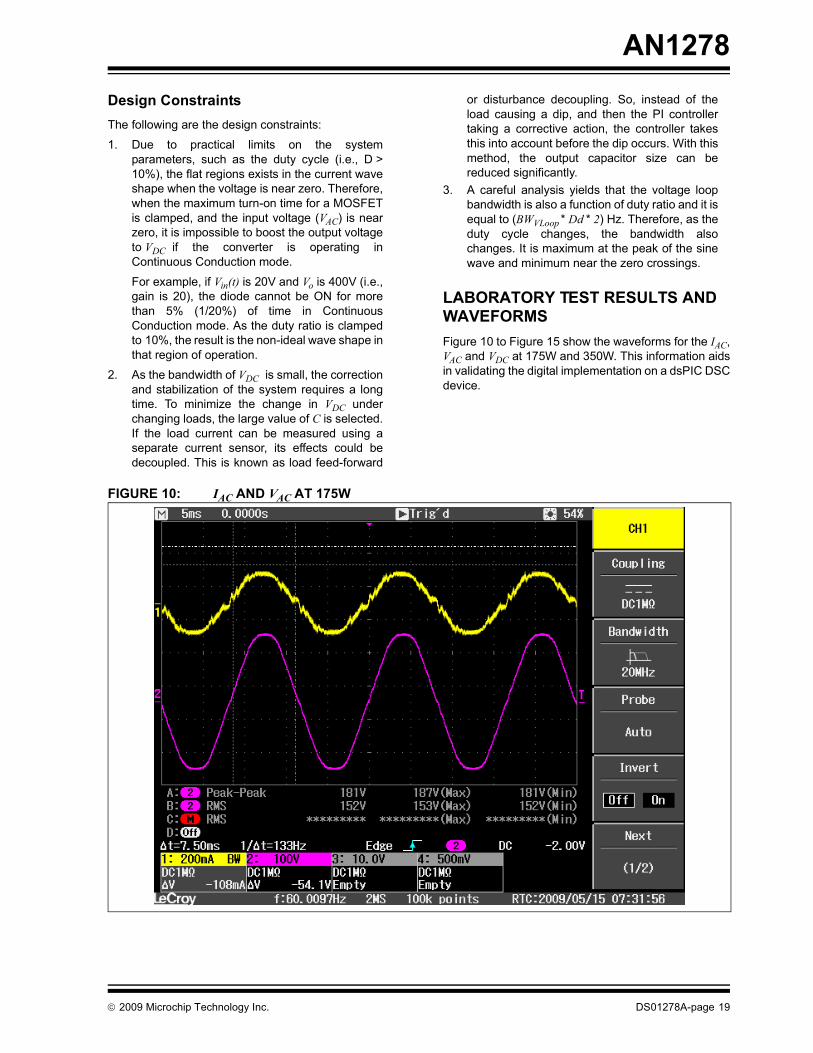
Figure 10 to Figure 15 show the waveforms for the IAC,VAC and VDC at 175W and 350W. This information aidsin validating the digital implementation on a dsPIC DSCdevice.
FIGURE 10: IAC AND VAC AT 175W
2009 Microchip Technology Inc. DS01278A-page 19

AN1278
FIGURE 11: IAC AND VAC AT 350W
FIGURE 12: IAC AND VAC TRANSIENT FROM 175W TO 350W
DS01278A-page 20 2009 Microchip Technology Inc.

AN1278
FIGURE 13: IAC AND VAC TRANSIENT FROM 350W TO 175W
FIGURE 14: 175W TO 350W VDC RESPONSE
2009 Microchip Technology Inc. DS01278A-page 21

AN1278
FIGURE 15: 350W TO 175W VDC RESPONSE
DS01278A-page 22 2009 Microchip Technology Inc.

AN1278
IPFC HARDWARE DESIGN
This section provides the hardware details and designguidelines. Figure 16 shows the block diagram of theIPFC system. The major hardware building blocks,shown in Figure 16, are discussed in this section. Thecore part of the IPFC system is the boost converterstage. The boost converter and various components ofthe system are designed to ensure system robustnessand versatility.
FIGURE 16: IPFC SYSTEM BLOCK DIAGRAM
FIGURE 17: EMI FILTER CIRCUIT
Note: For more information about manufactur-ers’ part numbers and data sheets, refer tothe Bill of Materials (BOM), which isincluded in the reference design archivefile (see Appendix A: “Source Code”).
EMI FilterAC
Rectifier
Signal Adaptation
dsPIC® DSCDebug Interface
Auxiliary Power Supply
Boost Converter
DC Output Power
AC Input Power
FUSE1SWITCH1
MOV1
C1
C2
C3 C4
R1
L1
G
L
N
2009 Microchip Technology Inc. DS01278A-page 23

AN1278
EMI Filter Block
The EMI filter located between the input terminals ofthe main supply and the AC rectifier circuitry is a singlestage quadruple type filter, which is designed to meetthe standards for conducted EMC. The input voltagerange of the EMI filter is 85-265 VAC. The output voltageof the EMI filter will be in the range of 85-265 VAC.
The simplified schematic of the EMI filter circuit is shownin Figure 17. L1 is a dual-wound toroidal inductor. C1 andC2, connected to the ground (G) are Y2 class compliantand meets the standards for the CATII overvoltage cate-gory. The choke (L1) and the capacitors (C1, C2) filter thecommon mode noise.
The choke (L1) offers a high impedance path to the in-phase component of the common mode noise, while C1and C2 shunt the high-frequency component of thenoise to the ground. The differential mode noise isfiltered using C3 and C4. The discharge resistor is usedwhen the circuit is plugged off. The varistor, MOV1, anda fuse provides overvoltage/overcurrent protection.
AC Rectifier Block
A diode bridge rectifies the input AC signal. It supportsthe rated AC input voltage (85-265 VAC) and thespecified power ratings. The rectifier block alsoprovides overcurrent protection using a NegativeTemperature Coefficient (NTC) thermistor.
Boost Converter Block
The boost converter contains IPFC stages and is fedfrom the rectifier's output. The simplified schematic ofthe boost converter circuit is shown in Figure 18. Theregulated output voltage of the converter is 400 VDC.
The converter contains two boost converter stages,which are parallel coupled and are 180º out of phasewith respect to each other. This configuration enablespower balancing between the two units. Thedimensioning of the circuit components depends on thespecified input/output voltages, power ratings, theiraccepted deviations and the available space on theboard layout. The dimensioning per stage is based onthe premise that at the maximum rated power, thesharing between the twin stages is equal.
INDUCTOR SELECTION (L2 and L3)
In addition to the parameters listed in the previous sec-tion, designing the boost inductors (L2 and L3) requiresconsideration of one more aspect: minimum peak volt-age available at the AC input terminals. The boost con-verter also boosts the minimum peak voltage up to therequired output voltage while meeting the load powerrequirements. The values of the inductor L2 and L3 arecomputed using Equation 19, which are considered asa first approximation of the inductance value.
EQUATION 19:
For IPFC circuit, I% is assumed to be 40% becauseripple cancellation is possible when the two stages are180º out of phase with respect to each other. For theminimum input voltage (85V), the required outputpower is 350W at 400 VDC. Equation 18 uses thesevalues and determines the value of L2 and L3.
EQUATION 20: INDUCTANCE CALCULATION
The choice of inductance often depends upon thetrade-off between the inductor value and the outputcurrent – a low inductance value results in a higheroutput current and a higher inductance value results inlower output current. If the smallest available value forthe inductor is chosen, the MOSFET and outputcapacitor will have to support a higher current andvoltages. Based on the result provided by Equation 20,an inductance of 700 µH is chosen for each booststage.
Note: The EMI/EMC filter value has beenchosen based on switching frequenciesand expected noise levels in the system.This value may be changed based on thefinal test results of EMI/EMC.
L2 L3Vin_min
2 T
I%Pout_max
2----------------------------------------------------
Vout Vin_min 2–Vout
------------------------------------------
= =
Vin_min = Minimum input voltage
Vout = Output DC voltage
T = Time period of the PWM switching
Pout_max = Maximum output power
Efficiency
I% = Ratio of accepted peak to peak inductor current ripple(typical value 20-40%)
where:
L2 L385
20.9 100
310
1–
40100---------
3502
----------------------------------------------------------------
400 85 2–400
---------------------------- = =
L2 L3 649.49 mH= =
DS01278A-page 24 2009 Microchip Technology Inc.

AN1278
FIGURE 18: INTERLEAVED BOOST CONVERTER CIRCUIT
MOSFET SELECTION
The selection of the MOSFETs (Q1 and Q3) dependson the specified output voltage of the IPFC system andthe maximum current that will pass through it (i.e., theinductor current). The output voltage (Vout) must belower than VDS rating of the MOSFET, while theinductor current (IL1 and IL2) should be lower than thedrain current (ID) rating of the MOSFET. The inductorcurrent can be computed using Equation 21.
EQUATION 21:
Equation 22 shows the inductance peak currentcalculation.
EQUATION 22: INDUCTANCE CURRENT CALCULATION
DIODE SELECTION (D1 AND D2)
The selection of the diodes (D1 and D2) depends onthe reverse recovery time (trr) and reverse voltagevalue (VRRM). The reverse recovery time determinesthe switch losses, which become significant at highercommutation frequencies. Because the losses in com-mutation are proportional with the time spent for eachcommutation, the reverse recovery time should be assmall as possible. The diodes D1 and D2, havingminimum reverse recovery time, are selected. Thereverse voltage rating of the selected diodes is higherthan the output voltage of the IPFC.
The efficiency of the IPFC denotes the acceptableoverall losses. Total power loss also includes lossesdue to the power semiconductors (i.e., losses in switch-ing and conduction). Equation 23 computes the powerloss for the given specifications.
EQUATION 23:
The selection of the power semiconductors, such asthe diodes and MOSFETs, also depends on the basiccharacteristics of the semiconductor device (i.e.,voltages and currents Characteristics) and the otherfeatures that indicates the losses in conduction orcommutation (e.g., reverse recovery time of the diodesand the drain source resistance of MOSFETs).
GATE 1
GATE 2
L2
L3 D2
D1
Q3
Q1
C6
D3
IL2 IL3
2Pout_max
2----------------------
Vin_min----------------------------- 1 I%
2-------+ = =
where:
Pout_max = Maximum output power
Vin_min = Minimum input voltage
Efficiency
IL2, IL3 = Inductance peak current
IL2 IL3
2 3502
---------
85 0.9------------------ 1
40100---------
2---------+
= =
IL2 IL3 3.88A= =
PL Pout1 –
------------- =
where:
PL = Power loss
Efficiency
Pout = Output Power
2009 Microchip Technology Inc. DS01278A-page 25
AN1278
Equation 22 expresses an approximation of the totalsemiconductor acceptable losses as being half of thetotal losses of the IPFC drive.
EQUATION 24:
CAPACITOR SELECTION (C6)
The selection of the output bulk capacitor (C6) dependson the acceptable output voltage ripple and theminimum holdup time considered for brown-outconditions. The holdup time (tholdup) is assumed to be15 ms, which is equivalent of power mains’ one semi-period power loss. The capacitance value can becomputed using Equation 25.
EQUATION 25:
The Effective Series Resistance (ESR) of the capacitoralso affects the output voltage ripple. Therefore, thecapacitor with the lowest possible ESR isrecommended. The ESR of the capacitor can belowered by coupling two capacitors in parallel if theboard layout dimensions permits. The resultantcapacitance of the parallel configuration should beequivalent to the capacitance, C6. However, theparalleling of the capacitors also results in division oftotal current ripple. Therefore, it lowers the currentripple specification per capacitor. Equation 26computes the power loss for the given specifications.
EQUATION 26: CAPACITOR CALCULATION
For this reference design, two 180 µF capacitors wereselected and are coupled in parallel.
DIODE SELECTION (D3)
To limit the start-up inrush current, the diode D3 shouldsupport the charging of the bulk capacitor current andthe reverse voltage, which is equal to the output voltage(Vout).
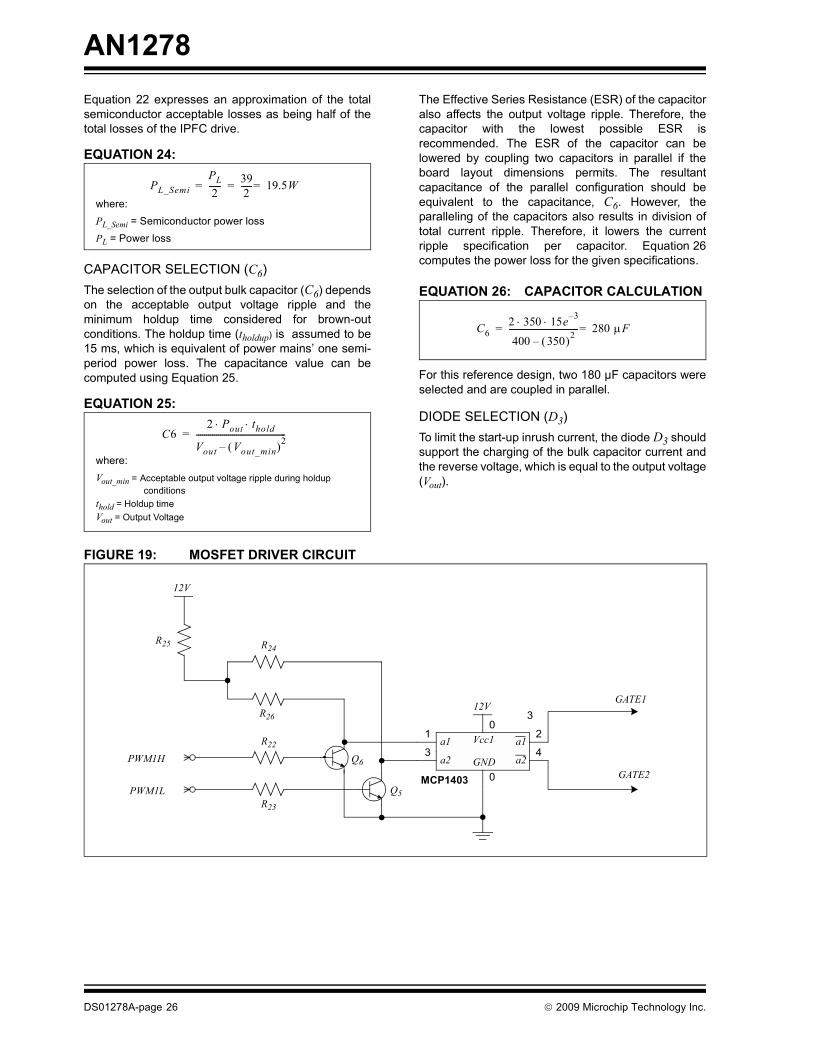
FIGURE 19: MOSFET DRIVER CIRCUIT
PL_Semi
PL
2------392------ 19.5W== =
where:
PL_Semi = Semiconductor power loss
PL = Power loss
C62 Pout thold
Vout Vout_min 2–---------------------------------------------=
where:
Vout_min = Acceptable output voltage ripple during holdup conditions
thold = Holdup time
Vout = Output Voltage
C62 350 15e
3–
400 350 2–----------------------------------- 280 F==
a11
a12Vcc1
03
a23
a24
GND
0
12V
12V
PWM1H
PWM1L
GATE1
GATE2
Q6
Q5
R25 R24
R26
R22
R23
MCP1403
DS01278A-page 26 2009 Microchip Technology Inc.

AN1278
Signal Adaptation Block
The signal adaptation block consists of all the electriccircuitry (active and passive), which interfaces thedsPIC DSC to the power electronics circuitry, such asMOSFET gate signals, analog currents and voltages,filters, and voltage dividers.
MOSFET GATE SIGNAL
The Microchip driver, MCP1403, drives the MOSFETgate signals: GATE1 and GATE2 (see Figure ).PWM1H and PWM1L are the output ports of the dsPICDSC device. When the base of the bipolar transistor(Q6) connected to PWM1H is high, the a1 input ofMCP1403 is low. Therefore, the output (a1) is drivenhigh (connected to GATE 1), and it opens the MOSFETtransistor Q1 (see Figure 18). The GATE2 operation issimilar to the GATE1 operation.
The signals acquisition includes the voltages andcurrents measurements. The IPFC system uses thefollowing methods for signal measurement and scaling:
Current Measurement Techniques:
• Shunt Current Measurement
• Current Transformer Measurement
Voltage Measurement Techniques:
• Resistive Divisor Voltage Measurement
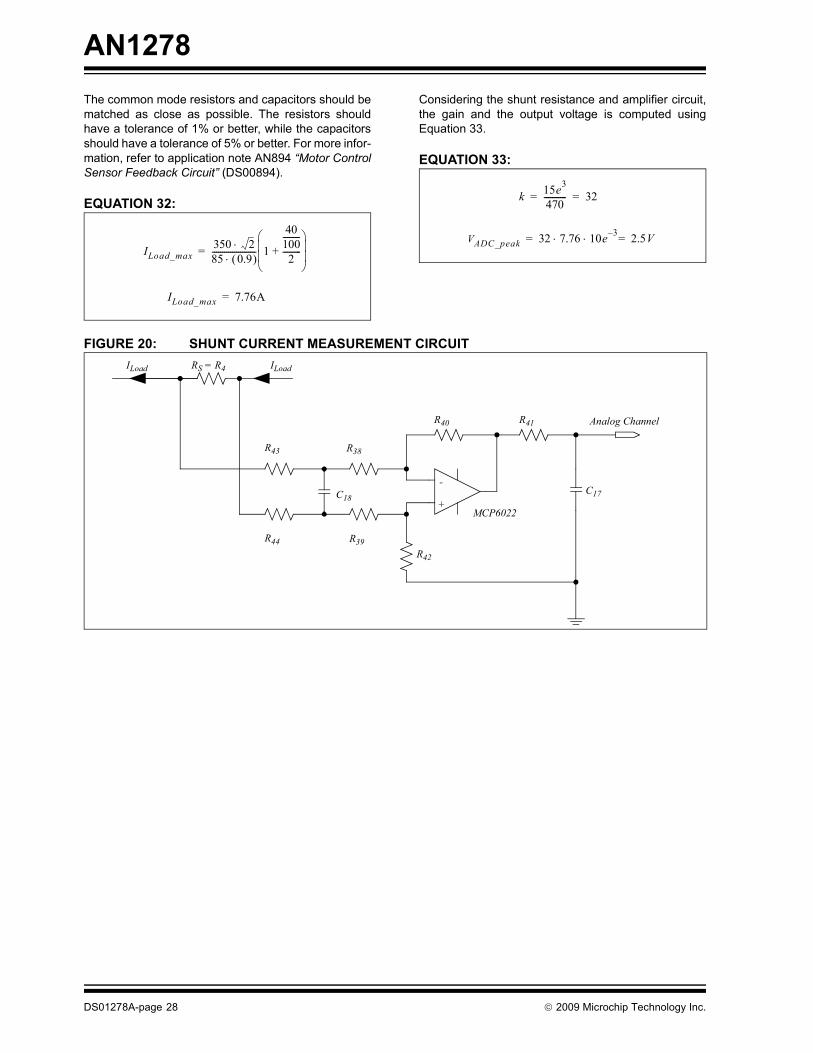
SHUNT CURRENT MEASUREMENT
This method measures the total current flowing into thesystem. In this method, the shunt (Rs) is connectedbetween the two boost stages and the input voltagerectifier. The load current passes through it.
The voltage drop on the shunt resistance is very small.It is amplified by differential amplifier and fed to theanalog channel of the ADC. The schematic is builtaround Microchip’s MCP6022 rail-to-rail input/outputOp amp, as shown in Figure 5, where ILoad designatesthe total current flowing to the load.
Equation 27 computes the cut-off frequency for thedifferential mode low-pass filter formed by the RCcombination R43, R44, and C18.
EQUATION 27:
For this circuit, R43 and R44 are chosen as 100 Ohmseach and C18 is chosen as 330 pF. Equation 28computes the cut-off frequency for the given componentvalues.
EQUATION 28:
The gain (k) of the circuit, shown in Figure 16, iscomputed using Equation 29.
EQUATION 29:
The gain is chosen such that the output voltage on theanalog pin of dsPIC DSC has sufficient tolerance underovercurrent condition and it is set in the range of 0V to3.3V. Equation 30 can be used to compute the outputvoltage.
EQUATION 30:
Equation 31 computes the cut-off frequency for theoutput low-pass filter formed by the RC combinationR41 and C17.
EQUATION 31:
f 3db–1
2 R43 R44+ C18 ---------------------------------------------------------=
f 3db–1
2 100 100+ 333 10 12– -----------------------------------------------------------------------------=
f 3db– 2.5 MHz=
kR40R38---------
R42R39---------==
R40R38---------
R42R39---------=
with the premise that:
VADC_peak k ILoad_maxRs =
ILoad_max
Pout_max 2Pin_max
--------------------------------- 1 I%2-------+
=
Where,
where:
VADC_peak = Maximum voltage on ADC pin
ILoad_max = Maximum load current
Pout_max = Maximum output power
Pin_max = Maximum input power
f 3db–1
2 R41 C17 -------------------------------------=
2009 Microchip Technology Inc. DS01278A-page 27
AN1278
The common mode resistors and capacitors should bematched as close as possible. The resistors shouldhave a tolerance of 1% or better, while the capacitorsshould have a tolerance of 5% or better. For more infor-mation, refer to application note AN894 “Motor ControlSensor Feedback Circuit” (DS00894).
EQUATION 32:
Considering the shunt resistance and amplifier circuit,the gain and the output voltage is computed usingEquation 33.
EQUATION 33:
FIGURE 20: SHUNT CURRENT MEASUREMENT CIRCUIT
ILoad_max350 285 0.9 ---------------------- 1
40100---------
2---------+
=
ILoad_max 7.76A=
k15e
3
470----------- 32= =
VADC_peak 32 7.76 10e3– 2.5V= =
RS = R4
R43 R38
R44 R39
R42
R40 R41
C17
Analog Channel
MCP6022
ILoad
C18
ILoad
-
+
DS01278A-page 28 2009 Microchip Technology Inc.
AN1278
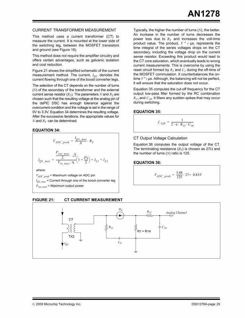
CURRENT TRANSFORMER MEASUREMENT
This method uses a current transformer (CT) tomeasure the current. It is mounted at the lower side ofthe switching leg, between the MOSFET transistorsand ground (see Figure 18).
This method does not require the amplifier circuitry andoffers certain advantages, such as galvanic isolationand cost reduction.
Figure 21 shows the simplified schematic of the currentmeasurement method. The current, IQ1, denotes thecurrent flowing through one of the boost converter legs.
The selection of the CT depends on the number of turns(N) of the secondary of the transformer and the externalcurrent sense resistor (RT). The parameters N and RT arechosen such that the resulting voltage at the analog pin ofthe dsPIC DSC has enough tolerance against theovercurrent condition and the voltage is set in the range of0V to 3.3V. Equation 34 determines the resulting voltage.After the successive iterations, the appropriate values forN and RT can be determined.
EQUATION 34:
Typically, the higher the number of turns (N), the better.An increase in the number of turns decreases thepower loss due to RT and increases the volt-timeproduct value. The product, V * t µs, represents thetime integral of the series voltages drops on the CTsecondary, including the voltage drop on the currentsense resistor. Exceeding this product would lead tothe CT core saturation, which eventually leads to wrongcurrent measurements. This is overcome by using thereset circuit formed by R1 and C1 during the off-time ofthe MOSFET commutation. It counterbalances the on-time V * t µs. Although, the balancing will not be perfect,it will ensure that the saturation does not occur.
Equation 35 computes the cut-off frequency for the CToutput low-pass filter formed by the RC combinationR13 and C10. It filters any sudden spikes that may occurduring switching.
EQUATION 35:
CT Output Voltage Calculation
Equation 36 computes the output voltage of the CT.The terminating resistance (RT) is chosen as 27 andthe number of turns (N) ratio is 125.
EQUATION 36:
FIGURE 21: CT CURRENT MEASUREMENT
VADC_peak
IQ1_max
N------------------- RT=
IQ1_max
Pout_max
2---------------------- 2
Vin_max ---------------------------------- 1 I%
2-------+ IL1 IL2===
where:
VADC_peak = Maximum voltage on ADC pin
IQ1_max = Current through one of the boost converter leg
Pout_max = Maximum output power
f 3db–1
2 R13 C10 -------------------------------------=
VADC_peak3.88125---------- 27 0.83V==
R13
C10
C9IQ1
R12
RT = R14
D4
CT
TX2
Analog Channel
2009 Microchip Technology Inc. DS01278A-page 29

AN1278
RESISTIVE DIVISOR VOLTAGE MEASUREMENT
The DC bus voltage and AC bus voltage required forthe control algorithm are scaled using the voltagedivisor shown in Figure 22.
In Figure 22, VACH and VACL are connected to thealternative input power lines, so that the peak inputvoltage is rectified using D10 and D11. The resistive divi-sor formed by R35 and R37 scales down the power linepeak voltage to the ADC input voltage level, which is inthe range of 0V to 3.3V. Equation 37 computes the gainof the voltage division.
EQUATION 37:
The capacitor C is used for the signal filtering, but itspresence in the circuit is not mandatory. Similarly, thepresence of the diode D3 is not mandatory. The diodeD3 provides protection if the voltage provided to ananalog pin of the dsPIC DSC exceeds 3.3V.
At the maximum input voltage, VADC_peak is computedusing Equation 38. For this circuit, R35 and R37 arechosen as 400 k and 3 k respectively.
EQUATION 38:
FIGURE 22: VOLTAGE DIVISORS – AC VOLTAGE SENSE
Auxiliary Power Supply Block
The auxiliary power supply is used to drive twovoltages:12V and 3.3V. It uses a TNY276P withFlyback topology and can handle input voltages in theuniversal range.
kR37
R35 R37+-----------------------=
VADC_peak k Vin_max=
Vin_peak Vin_max 2 265 2 373.65===
VADC_peak3
3 400+------------------ 373.65 2.78V==
where:
Vin_peak = Peak input voltage
VADC_peak = Maximum voltage on ADC pin
VADC_peak = Peak voltage on ADC pin
R35
C15
VACL
R37
D10
VACH
3.3V
D11
D12
Analog Channel
DS01278A-page 30 2009 Microchip Technology Inc.

AN1278
IPFC INSTALLATION AND CONFIGURATION
Overview of the IPFC Reference Design
The IPFC Reference Design is intended to aid the userin the rapid evaluation and development of PowerFactor Correction (PFC) using the dsPIC DSC.
This flexible and cost-effective tool can be configured indifferent ways for use with Microchip’s specializedSwitching Mode Power Supply (SMPS) Digital SignalControllers. The IPFC reference design supports thedsPIC33F motor control device family. It offers amounting option to connect either a 28-pin SOIC deviceor a generic 100-pin Plug-In Module (PIM).
The system has two PFC boost circuits to control thepower factor. The main components of the system areshown in Figure 1. The rated continuous output currentfrom the system is 1A (rms). This allows up to approxi-mately 350W output when running from an 85 VAC to265 VAC single-phase input voltage at a maximumambient temperature of 30ºC (85F).
For more details, refer to Appendix C: “ElectricalSpecifications”. Before using the IPFC system,carefully read the “IPFC Hardware Design” section.
KEY FEATURES
The key features of the IPFC Reference Design are:
• Devices Supported:
- 44-pin to 100-pin dsPIC33FJXXXGSX04 PIM (MA330020) with a dsPIC33F Motor Control device (U9) socket
- dsPIC33FJ06GS202 Motor Control device in 28-pin QFN-S package (U3) Footprint
• User Interfaces:
- LED indicators to indicate the following Fault conditions
- DC bus over-current fault (D14)- DC bus over-voltage fault (D17)- AC input over-voltage fault (D20)- AC input under-voltage fault (D22)- VDD Missing Fault (D24)
• LED indicators for Power Supply detection
- 12V (D33)
- DC bus (D13)
• Power ON/OFF switch (SW1)
• Minimum load ON/OFF switch (SW2)
• Push button (SW4)
• Push button (SW5)
• Push button (RESET)
• AC inlet connector (J1)
• Output connector (J2)
• Fan connector (FA1/JP11)
• Power supplies output connector (J12)
• Expansion connector (J5)
• RJ-11 connector for programming a dsPIC DSC device (J4), non-isolated
• ICSP™ connector for programming a dsPIC DSC device (J3), non-isolated
• Shunt jumper for internal/external power supply selection (J6)
• Shunt jumper for connecting/disconnecting the
- DC bus over-current fault (J7)
- DC bus over-voltage fault (J8)
- AC input over-voltage fault (J9)
- AC input under-voltage fault (J10)
- VDD missing fault (J11)
Power Factor Corrector:
• Implemented using two boost circuits in parallel (interleaved)
• Maximum output power: 350W at 400 VDC
• Maximum input voltage: 85-265 VAC
• Current feedback circuitry
• VAC input voltage sensing
• Zero-crossing detection
• DC bus sensing
• DC bus overcurrent protection
• DC bus overvoltage protection
• VAC input undervoltage protection
• VAC input overvoltage protection
Built-In power supplies
• 12V power supply
• 3.3V power supply
Additional Protection Circuitry
• 250 VAC/10A fuse
• In-rush current limiter
• EMI filter
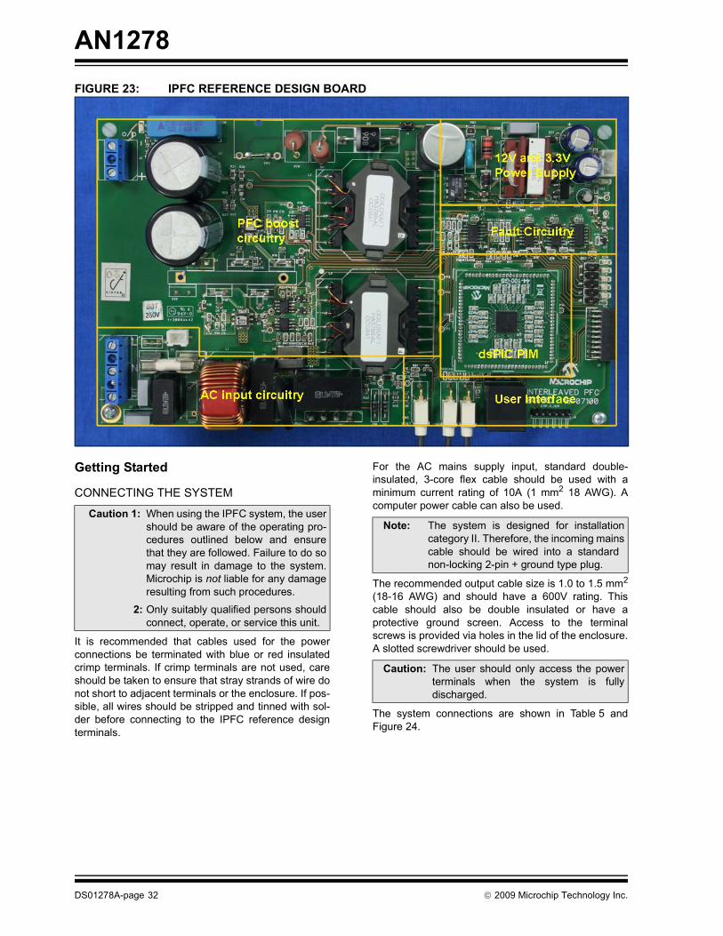
Figure 23 shows a photograph of the IPFC ReferenceDesign Board with key areas highlighted.
2009 Microchip Technology Inc. DS01278A-page 31
AN1278
FIGURE 23: IPFC REFERENCE DESIGN BOARD
Getting Started
CONNECTING THE SYSTEM
It is recommended that cables used for the powerconnections be terminated with blue or red insulatedcrimp terminals. If crimp terminals are not used, careshould be taken to ensure that stray strands of wire donot short to adjacent terminals or the enclosure. If pos-sible, all wires should be stripped and tinned with sol-der before connecting to the IPFC reference designterminals.
For the AC mains supply input, standard double-insulated, 3-core flex cable should be used with aminimum current rating of 10A (1 mm2 18 AWG). Acomputer power cable can also be used.
The recommended output cable size is 1.0 to 1.5 mm2
(18-16 AWG) and should have a 600V rating. Thiscable should also be double insulated or have aprotective ground screen. Access to the terminalscrews is provided via holes in the lid of the enclosure.A slotted screwdriver should be used.
The system connections are shown in Table 5 andFigure 24.
Caution 1: When using the IPFC system, the usershould be aware of the operating pro-cedures outlined below and ensurethat they are followed. Failure to do somay result in damage to the system.Microchip is not liable for any damageresulting from such procedures.
2: Only suitably qualified persons shouldconnect, operate, or service this unit.
Note: The system is designed for installationcategory II. Therefore, the incoming mainscable should be wired into a standard non-locking 2-pin + ground type plug.
Caution: The user should only access the powerterminals when the system is fullydischarged.
DS01278A-page 32 2009 Microchip Technology Inc.
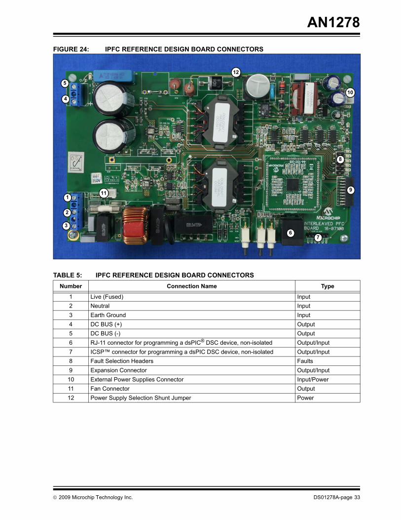
AN1278
FIGURE 24: IPFC REFERENCE DESIGN BOARD CONNECTORS
2
1
3
4
5
67
8
9
10
11
12
TABLE 5: IPFC REFERENCE DESIGN BOARD CONNECTORS
Number Connection Name Type
1 Live (Fused) Input
2 Neutral Input
3 Earth Ground Input
4 DC BUS (+) Output
5 DC BUS (-) Output
6 RJ-11 connector for programming a dsPIC® DSC device, non-isolated Output/Input
7 ICSP™ connector for programming a dsPIC DSC device, non-isolated Output/Input
8 Fault Selection Headers Faults
9 Expansion Connector Output/Input
10 External Power Supplies Connector Input/Power
11 Fan Connector Output
12 Power Supply Selection Shunt Jumper Power
2009 Microchip Technology Inc. DS01278A-page 33

AN1278
INTERCONNECTING THE HARDWARE
The recommended connection sequence is listedbelow. The user should ensure that the followingsequence is met before connecting the system to themains.
To set up the system, complete the following steps:
1. Connect the load to the DC BUS (+) and DCBUS (-) output terminals.
2. Make sure that the power cord is disconnectedfrom the AC mains before connecting it to theIPFC reference design AC input connector.
3. Connect the power cord to the Interleaved ACinlet.
4. Connect the power cord to the mains.
Power-up Sequence
To power-up the IPFC system, complete the followingsteps:
1. Connect the power cable to the AC mains.
2. Turn-on the incoming AC supply by sliding theswitch SW1 to the ON position.
3. Check the status of the D13 and D33 LEDs. Theunit is powered when these LEDs are ON.
Power-down Sequence
To disconnect the power supply to the IPFC system,complete the following steps:
1. Turn off the incoming AC supply by sliding theswitch SW1 to the OFF position.
2. Wait until the red DC bus LED indicator (D13)turns OFF. This can take a maximum of 5minutes.
3. Disconnect the power cord from mains.
PROGRAMMING/DEBUGGING AN APPLICATION CODE
The MPLAB® ICD 2, MPLAB IDC 3, PICkit™ 3 andMPLAB REAL ICE™ in-circuit emulator may be usedalong with MPLAB IDE to debug your software. MPLABIDE is the free integrated development environmentavailable from Microchip’s web site. MPLAB IDE allowsthese two devices, which are supported on the IPFCReference Design, to be used as an in-circuit debuggeras well as a programmer:
• dsPIC33FJ06GS202
• dsPIC33FJ16GS504
In-circuit debugging allows you to run, examine, andmodify your program for the device embedded in theIPFC system hardware. This greatly assists you indebugging your firmware and hardware together.
Special software interacts with the MPLAB IDEapplication to run, stop, and single-step through pro-grams. Breakpoints can be set and the processor canbe reset. Once the processor is stopped, the register’scontents can be examined and modified.
For more information on how to use MPLAB IDE, referto the following documentation:
• “MPLAB® IDE User’s Guide” (DS51519)
• “MPLAB® IDE Quick Start Guide” (DS51281)
• MPLAB® IDE Help File
SETTING UP AN APPLICATION FOR DEBUG
Complete the following steps to prepare the applicationfor debug:
1. Launch MPLAB IDE, and then open the applica-tion project. The related workspace will be open.For information on projects and workspaces,see the MPLAB IDE documentation mentionedat the beginning of this section.
2. Select Project>Build All to build the applicationcode. The build’s progress will be visible in theBuild tab of the Output window.
3. Select Debugger>Select Tool>”Your PreferredTool”. MPLAB IDE will change to add your tooldebug features.
4. Select Debugger>Program to program theapplication code into the dsPIC33F DSC device.The debug programming progress will be visiblein the Debugging tool tab of the Outputwindow.
PROGRAMMING AN APPLICATION
When the program is successfully debugged andrunning, the next step is to program the device forstandalone operation in the finished design. Whendoing this, the resources reserved for debug arereleased for use by the application. To program theapplication, use the following steps:
1. Disable your tool as a debug tool by selectingDebugger>Select Tool>None.
2. Select your tool as the programmer by selectingProgrammer>Select Programmer menu.
3. Select Programmer>Program.
Now the application code will run independently.
Note: Before making any connection verify thatthe system is not powered and is fullydischarged. The system is completelydischarged when the LED D13 is OFF.
Note: The programming connectors used forconnecting the MPLAB programmers/debuggers are not isolated. The usershould use an isolation method, such asan isolated USB HUB.
DS01278A-page 34 2009 Microchip Technology Inc.

AN1278
Running the Demonstration Software
To run the demonstration, complete the following steps:
1. On the IPFC Reference Design Board, makesure that the shunt jumper J6 is mounted.
2. Make sure that the dsPIC33FJ16GS504 PIM(MA330020) is mounted on the IPFC ReferenceDesign Board.
3. Connect the load to the DC BUS (+) and DCBUS (-). For details, refer to “Connecting theSystem”.
4. Power-on the IPFC reference design board,applying only 50V AC. For details, refer to“Power-up Sequence”.
5. Open the IPFC demonstration software bydouble-clicking the .mcw file.
6. After the MPLAB IDE work-bench is open, Com-pile the project. Build the project using the “BuildAll” option from the “Project” drop-down menu.(see Figure 25).
FIGURE 25: COMPILING CODE IN MPLAB® IDE
7. Select the programmer from the “Programmer”drop down menu. In this case select the MPLABREAL ICE or any of the other shown options.(see Figure 26).
FIGURE 26: PROGRAMMER SECTION IN MPLAB® IDE
FIGURE 27: PROGRAMMING OPTIONS IN MPLAB® IDE
8. Connect the programming tool to the IPFCReference Design Board using the RJ-11connector, and then program the device usingProgrammer>Program. Next, disconnect thedebugger from the board (see Figure 27).
9. Remove the programmer/debugger.
10. Increase the input voltage to the desired valuewithin the input range of 85-265V AC.
The IPFC Reference Design Board should now be upand running.
Note: The programming connectors used forconnecting the MPLAB programmers/debuggers are not isolated. User shoulduse an isolation method, such as anisolated USB HUB.
2009 Microchip Technology Inc. DS01278A-page 35

AN1278
CONCLUSION
This application note presents the novel method ofInterleaved Power Factor Correction (IPFC) using thedsPIC DSC. It explains in detail the digital design andimplementation of an IPFC converter including thehardware consideration and MATLAB simulations.
This unique approach can be used to design andintegrate other downstream converters following theIPFC stage. The power control-related peripherals,such as ADC, PWM, and Analog Comparators can beused for the other converter stages as well.
The modular design of the software makes it easier toappend other functions necessary to meet the needs ofthe specific application. The dsPIC DSC devices, withtheir high processing power and peripheral-richplatform, are well suited for development of suchcomplex applications on a single chip. Multiple controlloops running with different timing requirements can beexecuted using the variety of DSP instructions. Inaddition, the Data Monitor and Control Interface(DMCI) feature available in the MPLAB IntegratedDevelopment Environment (IDE) can be used to controland display the application variables while theapplication is running. This aids in observing varioussignals during the software development phase.
Microchip has various resources to assist you indeveloping this integrated application. For more detailson the IPFC Reference Design, please contact yourlocal Microchip Sales office.
REFERENCES
The following application notes have been published byMicrochip Technology Inc., which describe the use ofdsPIC DSC devices for power conversion applications:
• AN1106 “Power Factor Correction in Power Conversion Applications Using the dsPIC® DSC” (DS01106)
• AN1208 “Integrated Power Factor Correction (PFC) and Sensorless Field Oriented Control (FOC) System” (DS01208)
These documents are available for download from theMicrochip web site (www.microchip.com).
DS01278A-page 36 2009 Microchip Technology Inc.

AN1278
APPENDIX A: SOURCE CODE
All of the software covered in this application note isavailable as a single WinZip archive file. This archivecan be downloaded from the Microchip corporate Website at:
www.microchip.com
Software License AgreementThe software supplied herewith by Microchip Technology Incorporated (the “Company”) is intended and supplied to you, theCompany’s customer, for use solely and exclusively with products manufactured by the Company.The software is owned by the Company and/or its supplier, and is protected under applicable copyright laws. All rights are reserved.Any use in violation of the foregoing restrictions may subject the user to criminal sanctions under applicable laws, as well as to civilliability for the breach of the terms and conditions of this license.THIS SOFTWARE IS PROVIDED IN AN “AS IS” CONDITION. NO WARRANTIES, WHETHER EXPRESS, IMPLIED OR STATU-TORY, INCLUDING, BUT NOT LIMITED TO, IMPLIED WARRANTIES OF MERCHANTABILITY AND FITNESS FOR A PARTICU-LAR PURPOSE APPLY TO THIS SOFTWARE. THE COMPANY SHALL NOT, IN ANY CIRCUMSTANCES, BE LIABLE FORSPECIAL, INCIDENTAL OR CONSEQUENTIAL DAMAGES, FOR ANY REASON WHATSOEVER.
2009 Microchip Technology Inc. DS01278A-page 37

AN1278
APPENDIX B: SYMBOL GLOSSARY TABLE B-1: SYMBOLS AND DESCRIPTIONS
Symbol Description
VAC Rectified AC Voltage
IAC Rectified AC Current
VDC DC Bus Voltage
VDCREF DC Bus Reference Voltage
IACREF Capacitor Current Reference
Rmax Maximum Resistance
Vmax Maximum Voltage
Imax Maximum Current
max Maximum Conductance
Ga Proportional Gain for Voltage Error Compensator
Gsa Integral Gain for Voltage Error Compensator
BWVLoop Voltage Loop Bandwidth
IBWVLoop Integral Voltage Loop Bandwidth
fVLoop Voltage Control Loop Frequency
Ra Proportional Gain for Current Error Compensator
Rsa Integral Gain for Current Error Compensator
BWILoop Current Loop Bandwidth
IBWILoop Integral Current Loop Bandwidth
fILoop Current Control Loop Frequency
Ka Proportional Gain for Load Balance Error Compensator
Ksa Integral Gain for Load Balance Error Compensator
BWLBLoop Load Balance Loop Bandwidth
IBWLBLoop Integral Load Balance Loop Bandwidth
fLBLoop Load Balance Control Loop Frequency
VAVG Average Value of the Rectified Input Voltage
VL Inductor Voltage obtained from the current error compensator
D Main Duty cycle
D1 Duty Cycle of MOSFET1
D2 Duty Cycle of MOSFET2
Dd Main Duty cycle
DD Correction in Duty Cycle
ESinglestage Energy stored in a single stage PFC converter
EInterleaved Energy stored in a IPFC converter
Ki Proportional Gain
Kv Integral Gain
Vin_min Minimum input voltage
Vout Output DC voltage
T Time period of the PWM switching
Pout_max Maximum output power
h Efficiency
I% Ratio of accepted peak to peak inductor current ripple (typical value 20-40%)
DS01278A-page 38 2009 Microchip Technology Inc.

AN1278
thold Holdup time
trr Reverse recovery time
VRRM Reverse voltage value
Vout_min Minimum output voltage
ESR Effective series resistance
VADC_peak Maximum voltage on ADC pin
T Time period of the PWM switching
Pout_max Maximum output power
h Efficiency
I% Ratio of accepted peak-to-peak inductor current ripple (typical value 20-40%)
thold Holdup time
trr Reverse recovery time
VRRM Reverse voltage value
Vout_min Minimum output voltage
ESR Effective series resistance
VADC_peak Maximum voltage on ADC pin
Vin_peak Input Peak Voltage
Vin_max Maximum Input Voltage
IQ1max Current flowing through Boost Converter Leg
L Effective Boost Inductance
C Effective Boost Capacitance
IM1 MOSFET1 current
IM2 MOSFET2 current
VERR Voltage Error
ICAPREF Capacitor Current Reference
IINDREF Inductor Current Reference
IERR Current Error
VIND Inductor Current
VL Inductor Voltage obtained from the current error compensator
IC Current through Output Capacitor
ID Diode Current
tON ON time of the MOSFET
tOFF OFF time of the MOSFET
VDCREF Reference DC Voltage
VDC Sensed DC Voltage
ILoad Load Current
ILoad_max Maximum Load Current
IACREF Reference current signal
Vm Peak voltage of half sine wave
Vavg Average voltage
VL Inductor voltage
TABLE B-1: SYMBOLS AND DESCRIPTIONS (CONTINUED)
Symbol Description
2009 Microchip Technology Inc. DS01278A-page 39

AN1278
APPENDIX C: ELECTRICAL SPECIFICATIONS
The IPFC Reference Design was tested at a maximumpower of 350W with resistive and a three-phaseinverter type load.
TABLE C-1: ELECTRICAL SPECIFICATIONS
Parameter Minimum
Typical Values at120 VAC Input
400 VDC Output350W Output
Typical Values at230 VAC Input
400 VDC Output350W Output
Maximum
Input Voltage 85 VAC 120 VAC 230 VAC 265 VAC
Input Current — 3.17A 1.6A 8A
Input Power — 380W 368W 400W
Output Voltage — 400 VDC ± 2% 400 VDC ± 2% 420 VDC
Output Current — 0.87A 0.87A 2A
Output Power — 350W 350W 350W
Heatsink at 25ºC Ambient Temperature
— 70ºC(1) 48ºC(1) 75ºC(2)
ITHD — 3% 5% —
Power Factor — 0.998 0.992 —
Efficiency — 92% 95% —
Note 1: When using a heatsink with a thermal resistance of 6ºC/W, the heatsink temperature stabilizes at this valuefor continuous operation.
2: The temperature was measured on the heatsink after one hour of operation at a minimum input voltage of85 VAC and maximum output power of 350W at 400 VDC. No fan was utilized. If the user requires full dutycycle operation under these conditions, an external fan is recommended to keep the heatsink temperaturebelow 75ºC.
DS01278A-page 40 2009 Microchip Technology Inc.

AN1278
APPENDIX D: SCHEMATICS AND BOARD LAYOUT
FIGURE D-1: IPFC REFERENCE DESIGN SCHEMATIC (SHEET 1 OF 3)
BO
OS
T C
ON
VE
RT
ER
ST
AG
E
2009 Microchip Technology Inc. DS01278A-page 41

AN1278
FIGURE D-2: IPFC REFERENCE DESIGN SCHEMATIC (SHEET 2 OF 3)
12
V/0
.4A
DE
BU
GG
ER
INT
ER
FA
CE
AU
XIL
IAR
Y S
UP
PL
Y
AN
6/O
SC
1
LO
WR
EF
AN
7/O
SC
0
DS01278A-page 42 2009 Microchip Technology Inc.

AN1278
FIGURE D-3: IPFC REFERENCE DESIGN SCHEMATIC (SHEET 3 OF 3)
HA
RD
WA
RE
FA
UL
T P
RO
TE
CT
ION
FO
R D
EV
ELO
PM
EN
T P
UR
PO
SE
ON
LY
2009 Microchip Technology Inc. DS01278A-page 43
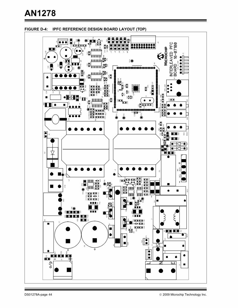
AN1278
FIGURE D-4: IPFC REFERENCE DESIGN BOARD LAYOUT (TOP)
DS01278A-page 44 2009 Microchip Technology Inc.

Note the following details of the code protection feature on Microchip devices:
• Microchip products meet the specification contained in their particular Microchip Data Sheet.
• Microchip believes that its family of products is one of the most secure families of its kind on the market today, when used in the intended manner and under normal conditions.
• There are dishonest and possibly illegal methods used to breach the code protection feature. All of these methods, to our knowledge, require using the Microchip products in a manner outside the operating specifications contained in Microchip’s Data Sheets. Most likely, the person doing so is engaged in theft of intellectual property.
• Microchip is willing to work with the customer who is concerned about the integrity of their code.
• Neither Microchip nor any other semiconductor manufacturer can guarantee the security of their code. Code protection does not mean that we are guaranteeing the product as “unbreakable.”
Code protection is constantly evolving. We at Microchip are committed to continuously improving the code protection features of ourproducts. Attempts to break Microchip’s code protection feature may be a violation of the Digital Millennium Copyright Act. If such actsallow unauthorized access to your software or other copyrighted work, you may have a right to sue for relief under that Act.
Information contained in this publication regarding deviceapplications and the like is provided only for your convenienceand may be superseded by updates. It is your responsibility toensure that your application meets with your specifications.MICROCHIP MAKES NO REPRESENTATIONS ORWARRANTIES OF ANY KIND WHETHER EXPRESS ORIMPLIED, WRITTEN OR ORAL, STATUTORY OROTHERWISE, RELATED TO THE INFORMATION,INCLUDING BUT NOT LIMITED TO ITS CONDITION,QUALITY, PERFORMANCE, MERCHANTABILITY ORFITNESS FOR PURPOSE. Microchip disclaims all liabilityarising from this information and its use. Use of Microchipdevices in life support and/or safety applications is entirely atthe buyer’s risk, and the buyer agrees to defend, indemnify andhold harmless Microchip from any and all damages, claims,suits, or expenses resulting from such use. No licenses areconveyed, implicitly or otherwise, under any Microchipintellectual property rights.
2009 Microchip Technology Inc.
Trademarks
The Microchip name and logo, the Microchip logo, dsPIC, KEELOQ, KEELOQ logo, MPLAB, PIC, PICmicro, PICSTART, rfPIC and UNI/O are registered trademarks of Microchip Technology Incorporated in the U.S.A. and other countries.
FilterLab, Hampshire, HI-TECH C, Linear Active Thermistor, MXDEV, MXLAB, SEEVAL and The Embedded Control Solutions Company are registered trademarks of Microchip Technology Incorporated in the U.S.A.
Analog-for-the-Digital Age, Application Maestro, CodeGuard, dsPICDEM, dsPICDEM.net, dsPICworks, dsSPEAK, ECAN, ECONOMONITOR, FanSense, HI-TIDE, In-Circuit Serial Programming, ICSP, ICEPIC, Mindi, MiWi, MPASM, MPLAB Certified logo, MPLIB, MPLINK, mTouch, nanoWatt XLP, Omniscient Code Generation, PICC, PICC-18, PICkit, PICDEM, PICDEM.net, PICtail, PIC32 logo, REAL ICE, rfLAB, Select Mode, Total Endurance, TSHARC, WiperLock and ZENA are trademarks of Microchip Technology Incorporated in the U.S.A. and other countries.
SQTP is a service mark of Microchip Technology Incorporated in the U.S.A.
All other trademarks mentioned herein are property of their respective companies.
© 2009, Microchip Technology Incorporated, Printed in the U.S.A., All Rights Reserved.
Printed on recycled paper.
DS01278A-page 45
Microchip received ISO/TS-16949:2002 certification for its worldwide headquarters, design and wafer fabrication facilities in Chandler and Tempe, Arizona; Gresham, Oregon and design centers in California and India. The Company’s quality system processes and procedures are for its PIC® MCUs and dsPIC® DSCs, KEELOQ® code hopping devices, Serial EEPROMs, microperipherals, nonvolatile memory and analog products. In addition, Microchip’s quality system for the design and manufacture of development systems is ISO 9001:2000 certified.

DS01278A-page 46 2009 Microchip Technology Inc.
AMERICASCorporate Office2355 West Chandler Blvd.Chandler, AZ 85224-6199Tel: 480-792-7200 Fax: 480-792-7277Technical Support: http://support.microchip.comWeb Address: www.microchip.com
AtlantaDuluth, GA Tel: 678-957-9614 Fax: 678-957-1455
BostonWestborough, MA Tel: 774-760-0087 Fax: 774-760-0088
ChicagoItasca, IL Tel: 630-285-0071 Fax: 630-285-0075
ClevelandIndependence, OH Tel: 216-447-0464 Fax: 216-447-0643
DallasAddison, TX Tel: 972-818-7423 Fax: 972-818-2924
DetroitFarmington Hills, MI Tel: 248-538-2250Fax: 248-538-2260
KokomoKokomo, IN Tel: 765-864-8360Fax: 765-864-8387
Los AngelesMission Viejo, CA Tel: 949-462-9523 Fax: 949-462-9608
Santa ClaraSanta Clara, CA Tel: 408-961-6444Fax: 408-961-6445
TorontoMississauga, Ontario, CanadaTel: 905-673-0699 Fax: 905-673-6509
ASIA/PACIFICAsia Pacific OfficeSuites 3707-14, 37th FloorTower 6, The GatewayHarbour City, KowloonHong KongTel: 852-2401-1200Fax: 852-2401-3431
Australia - SydneyTel: 61-2-9868-6733Fax: 61-2-9868-6755
China - BeijingTel: 86-10-8528-2100 Fax: 86-10-8528-2104
China - ChengduTel: 86-28-8665-5511Fax: 86-28-8665-7889
China - Hong Kong SARTel: 852-2401-1200 Fax: 852-2401-3431
China - NanjingTel: 86-25-8473-2460Fax: 86-25-8473-2470
China - QingdaoTel: 86-532-8502-7355Fax: 86-532-8502-7205
China - ShanghaiTel: 86-21-5407-5533 Fax: 86-21-5407-5066
China - ShenyangTel: 86-24-2334-2829Fax: 86-24-2334-2393
China - ShenzhenTel: 86-755-8203-2660 Fax: 86-755-8203-1760
China - WuhanTel: 86-27-5980-5300Fax: 86-27-5980-5118
China - XiamenTel: 86-592-2388138 Fax: 86-592-2388130
China - XianTel: 86-29-8833-7252Fax: 86-29-8833-7256
China - ZhuhaiTel: 86-756-3210040 Fax: 86-756-3210049
ASIA/PACIFICIndia - BangaloreTel: 91-80-3090-4444 Fax: 91-80-3090-4080
India - New DelhiTel: 91-11-4160-8631Fax: 91-11-4160-8632
India - PuneTel: 91-20-2566-1512Fax: 91-20-2566-1513
Japan - YokohamaTel: 81-45-471- 6166 Fax: 81-45-471-6122
Korea - DaeguTel: 82-53-744-4301Fax: 82-53-744-4302
Korea - SeoulTel: 82-2-554-7200Fax: 82-2-558-5932 or 82-2-558-5934
Malaysia - Kuala LumpurTel: 60-3-6201-9857Fax: 60-3-6201-9859
Malaysia - PenangTel: 60-4-227-8870Fax: 60-4-227-4068
Philippines - ManilaTel: 63-2-634-9065Fax: 63-2-634-9069
SingaporeTel: 65-6334-8870Fax: 65-6334-8850
Taiwan - Hsin ChuTel: 886-3-6578-300Fax: 886-3-6578-370
Taiwan - KaohsiungTel: 886-7-536-4818Fax: 886-7-536-4803
Taiwan - TaipeiTel: 886-2-2500-6610 Fax: 886-2-2508-0102
Thailand - BangkokTel: 66-2-694-1351Fax: 66-2-694-1350
EUROPEAustria - WelsTel: 43-7242-2244-39Fax: 43-7242-2244-393Denmark - CopenhagenTel: 45-4450-2828 Fax: 45-4485-2829
France - ParisTel: 33-1-69-53-63-20 Fax: 33-1-69-30-90-79
Germany - MunichTel: 49-89-627-144-0 Fax: 49-89-627-144-44
Italy - Milan Tel: 39-0331-742611 Fax: 39-0331-466781
Netherlands - DrunenTel: 31-416-690399 Fax: 31-416-690340
Spain - MadridTel: 34-91-708-08-90Fax: 34-91-708-08-91
UK - WokinghamTel: 44-118-921-5869Fax: 44-118-921-5820
WORLDWIDE SALES AND SERVICE
03/26/09