Embed Size (px)
Citation preview

Fre
esc
ale
Se
mic
on
du
cto
r, I
nc
...
Order this documentby AN1745/D
AN1745
Interfacing the HC705C8A to an LCD ModuleBy Mark Glenewinkel
Consumer Systems GroupAustin, Texas
Introduction
More and more applications are requiring liquid crystal displays (LCD) toeffectively communicate to the outside world. This application notedescribes the hardware and software interface needed to displayinformation from the MC68HC705C8A.
Some LCD suppliers provide only the LCD glass so that the waveformsneeded to directly drive the LCD segments have to be generated by themicrocontroller (MCU) or microprocessor (MPU). Other LCD suppliersprovide an LCD module, which has all LCD glass and segment driversprovided in one small packaged circuit board.
This application note uses an LCD module from Optrex, part numberDMC16207 (207). It utilizes a Hitachi LCD driver, HD44780, to providethe LCD segment waveforms and a simple parallel port interface thateasily interfaces to an MCU or MPU bus.
Circuitry and example code are given to also demonstrate the ability ofproviding pre-defined messages from EPROM memory. The code canbe easily modified to take serial peripheral interface (SPI) and serialcommunication interface (SCI) data and display it on the LCD module.
© Motorola, Inc., 1998 AN1745
For More Information On This Product, Go to: www.freescale.com

Application Note
F
ree
sca
le S
em
ico
nd
uc
tor,
I
Freescale Semiconductor, Inc.n
c..
.
LCD Module Hardware Interface
Optrex has many LCD module configurations that have varying displaylines and display line character lengths. The 207 module has a 2-line,16-character/line display. Each character is displayed using a 5 x 7 pixelfont matrix. The 207 module has a character generator ROM capable ofdisplaying ASCII characters.
The parallel interface bus can work with either 4-bit or 8-bit buses. Oncedata is presented on the bus, it is latched by clocking the E pin on thedevice. Depending on the RS pin, the data will be used as an instructionor an ASCII character.
Pin Descriptions Table 1 describes the interface pins found on the 207 module.
Table 1. 207 Module Pinout
Pin no. Signal I/O Function
1 VSS Power GND (ground)
2 VCC Power 2.7 V to 5.5 V
3 VEE Power LCD drive voltage
4 RS I
Selects registers0: Instruction register (for write), address counter
(for read)1: Data register (for write and read)
5 R/W ISelects read or write0: Write1: Read
6 E I Starts data read/write on falling edge
14–11 DB7–DB4 I/O
Four high-order bidirectional three-state data buspins. Used for data transfer and receivebetween the MCU and the 207. DB7 can beused as a busy flag.
10–7 DB3–DB0 I/O
Four low-order bidirectional three-state data buspins. Used for data transfer and receivebetween the MCU and the 207. These pins arenot used during 4-bit operation.
AN1745
2 For More Information On This Product,
Go to: www.freescale.com

Application NoteLCD Module Hardware Interface
F
ree
sca
le S
em
ico
nd
uc
tor,
I
Freescale Semiconductor, Inc.n
c..
.
Bus Timing
Figure 1. Write Timing Operation
Table 2. Bus Timing Electricals
Characteristic Symbol Min Typ Max Unit
Enable cycle time tCYCE 500 — — ns
Enable pulse width (high level) PWEH 230 — — ns
Enable rise and decay time tEr, tEf — — 20 ns
Address setup time, RS, R/W, E tAS 40 — — ns
Data delay time tDDR — — 160 ns
Data setup time tDSW 80 — — ns
Data hold time (write) tH 10 — — ns
Data hold time (read) tDHR 5 — — ns
Address hold time tAH 10 — — ns
RS
R/W
E
DB0–DB7
tAS tAH
tCYCE
PWEH
tEr
tEf
tDSW tH
VALID DATA
AN1745
3 For More Information On This Product,
Go to: www.freescale.com

Application Note
F
ree
sca
le S
em
ico
nd
uc
tor,
I
Freescale Semiconductor, Inc.n
c..
.
Figure 2. Read Timing Operation
Bus Interface Figure 3 and Figure 4 show examples of 8-bit and 4-bit timingsequences, respectively. Note that a BF check is not needed if themaximum instruction execution time is respected before sendinganother instruction.
Figure 3. 8-Bit Bus Timing Sequence
RS
R/W
E
DB0–DB7
tAS tAH
tCYCE
PWEH
tEr
tEf
tDDR tDHR
VALID DATA
RS
R/W
E
INTERNAL
DB7–DB0 DATA
OPERATION
BUSYNOT BUSY DATA
INSTRUCTIONWRITE
BUSY FLAGCHECK
BUSY FLAGCHECK
INSTRUCTIONWRITE
EXEC TIME
AN1745
4 For More Information On This Product,
Go to: www.freescale.com

Application NoteLCD Module Hardware Interface
F
ree
sca
le S
em
ico
nd
uc
tor,
I
Freescale Semiconductor, Inc.n
c..
.
For 4-bit interface data, only four bus lines (DB7–DB4) are used fortransfer. Bus lines DB3–DB0 are disabled. The data transfer iscompleted after the 4-bit data has been transferred twice. The four high-order bits are transferred first (DB7–DB4), and then the low-order bitsare transferred (DB3–DB0).
Figure 4. 4-Bit Bus Timing Sequence
RS
R/W
E
D7–D4 D3–D0 BUSY AC3
NOT
INSTRUCTION WRITE INSTRUCTION WRITE
EXEC TIME
BUSY FLAGCHECK
BUSY AC3 D7–D4 D3–D0
BUSY FLAGCHECK
INTERNAL
DB7–DB0
OPERATION
AN1745
5 For More Information On This Product,
Go to: www.freescale.com

Application Note
F
ree
sca
le S
em
ico
nd
uc
tor,
I
Freescale Semiconductor, Inc.n
c..
.
LCD Module Software Interface
LCD InstructionCommands
The 207 module has many different configurations that can be easilyimplemented by sending the correct function command to the device.These commands are listed in Table 3 followed by an explanation ofeach function they execute.
Clear Display Clear display writes space code $20 into all DDRAM addresses. It thensets DDRAM address 0 into the address counter and returns the displayto its original status if it was shifted. In other words, the displaydisappears and the cursor or blinking goes to the left edge of the first lineof the display. I/D of entry mode is set to 1 (increment mode). S of entrymode is left unchanged.
Table 3. 207 Module Instruction Code
Instruction RS R W DB7 DB6 DB5 DB4 DB3 DB2 DB1 DB0 Executiontime (max)
Clear display 0 0 0 0 0 0 0 0 0 1 1.64 ms
Return cursor home 0 0 0 0 0 0 0 0 1 x 1.64 ms
Entry mode set 0 0 0 0 0 0 0 1 I/D S 40 µs
Display on/off ctrl 0 0 0 0 0 0 1 D C B 40 µs
Cursor or display shift 0 0 0 0 0 1 S/C R/L x x 40 µs
Function set 0 0 0 0 1 DL N F x x 40 µs
Set CGRAM address 0 0 0 1 ACG ACG ACG ACG ACG ACG 40 µs
Set DDRAM address 0 0 1 ADD ADD ADD ADD ADD ADD ADD 40 µs
Read busy flag &addr 0 1 BF AC AC AC AC AC AC AC 0 µs
Write data to CGor DDRAM
1 0 D7 D6 D5 D4 D3 D2 D1 D0 40 µs
Read data from CGor DDRAM
1 1 D7 D6 D5 D4 D3 D2 D1 D0 40 µs
DDRAM: Display data RAMCGRAM: Character generator RAMACG: CGRAM addressADD: DDRAM address; corresponds to cursor addressAC: Address counter used for both DDRAM and CGRAM addresses
AN1745
6 For More Information On This Product,
Go to: www.freescale.com

Application NoteLCD Module Software Interface
F
ree
sca
le S
em
ico
nd
uc
tor,
I
Freescale Semiconductor, Inc.n
c..
.
Return CursorHome
Return cursor home sets the DDRAM address 0 into the address counterand returns the display to its original status if it was shifted. The DDRAMcontents do not change.
The cursor or blinking goes to the left edge of the first line of the display.
Entry Mode Set I/D — Increments (I/D = 1) or decrements (I/D = 0) the DDRAM addressby 1 when a character code is written into or read from DDRAM. Thecursor or blinking moves to the right when incremented by 1 and to theleft when decremented by 1. The same applies to writing and readingof CGRAM.
S — Shifts the entire display either to the right (ID = 0) or to the left(I/D = 1) when S is 1. The display does not shift if S is 0. If S is 1, it willseem as if the cursor does not move but the display does. The displaydoes not shift when reading from DDRAM. Also, writing into or readingout from CGRAM does not shift the display.
Display On/OffControl
D — The display is on when D = 1 and is off when D = 0. When off, thedisplay data remains in DDRAM, but can be displayed instantly bysetting D = 1.
C — The cursor is displayed when C = 1 and not displayed when C = 0.Even if the cursor disappears, the function of I/D or other specificationswill not change during display data write. The cursor is displayed usingfive dots in the eighth line of the 5 x 8 dot character.
B — The character indicated by the cursor blinks when B = 1. Theblinking is displayed as switching between all blank dots and displayedcharacters at a speed of 409.6-ms intervals when fOSC (HD44780operating frequency) is 250 kHz. The cursor and blinking can beset to display simultaneously. (The blinking frequency changesaccording to fOSC. For example, when fOSC, is 270 kHz,409.6 x (250/270) = 379.2 ms.)
Cursor or DisplayShift
Cursor or display shift shifts the cursor position or display to the right orleft without writing or reading display data. See Table 4 .This function isused to correct or search the display. In a 2-line display, the cursor
AN1745
7 For More Information On This Product,
Go to: www.freescale.com

Application Note
F
ree
sca
le S
em
ico
nd
uc
tor,
I
Freescale Semiconductor, Inc.n
c..
.
moves to the second line when it passes the 40th digit of the first line.The first and second line displays will shift at the same time.
When the displayed data is shifted repeatedly, each line moves onlyhorizontally. The second line display does not shift into the first lineposition.
The address counter (AC) contents will not change if the only actionperformed is a display shift.
Function Set DL — Sets the interface data length. Data is sent or received in 8-bitlengths (DB7 to DB0) when DL = 1, and in 4-bit lengths (DB7 to DB4)when DL = 0. When 4-bit length is selected, data must be sent orreceived twice.
N — Sets the number of display lines
F — Sets the character font
NOTE: Perform the function set instruction at the beginning of the programbefore executing any instructions (except for the read busy flag andaddress instruction). From this point, the function set instruction cannotbe executed unless the interface data length is changed.
Set CGRAMAddress
Set CGRAM address sets the CGRAM binary address ACG5–ACG0 intothe address counter. Data is written to or read from the MCU forCGRAM.
Table 4. Cursor and Display Shift Combination
S/C R/L Description
0 0 Shifts the cursor position to the left; AC is decremented by 1
0 1 Shifts the cursor position to the right; AC is incremented by 1
1 0 Shifts the entire display to the left; he cursor follows the display shift
1 1 Shifts the entire display to the right; he cursor follows the display shift
AN1745
8 For More Information On This Product,
Go to: www.freescale.com

Application NoteLCD Module Software Interface
F
ree
sca
le S
em
ico
nd
uc
tor,
I
Freescale Semiconductor, Inc.n
c..
.
Set DDRAMAddress
Set DDRAM address sets the DDRAM binary address ADD6–ADD0 intothe address counter. Data is written to or read from the MCU forDDRAM.
Read Busy Flagand Address
Read busy flag and address reads the busy flag (BF) indicating that thesystem is now internally operating on a previously received instruction.If BF = 1, the internal operation is in progress. The next instruction willnot be accepted until BF is reset to 0. Check the BF status before thenext write operation. At the same time, the value of the address counterin binary (AC6–AC0) is read out. This address counter is used by bothCGRAM and DDRAM addresses, and its value is determined by theprevious instruction. The address contents are the same as forinstructions set CGRAM address and set DDRAM address.
Write Datato CGRAMor DDRAM
Write data to CGRAM or DDRAM writes 8-bit data to CGRAM orDDRAM. To write into CGRAM or DDRAM is determined by the previousspecification of the CGRAM or DDRAM address setting. After a write,the address is incremented or decremented automatically by 1according to the entry mode. The entry mode also determines thedisplay shift.
Read Datafrom CGRAMor DDRAM
Read data from CGRAM or DDRAM reads 8-bit data from CGRAM orDDRAM. The previous designation determines whether CGRAM orDDRAM is to be read. Before entering this read instruction, eitherCGRAM or DDRAM address set instruction must be executed. If notexecuted, the first read data will be invalid. When serially executing readinstructions, the next address data is normally read from the secondread. The address set instructions need not be executed just before thisread instruction when shifting the cursor by the cursor shift instruction(when reading out of DDRAM). The operation of the cursor shiftinstruction is the same as the set DDRAM address instruction. After aread, the entry mode automatically increases or decreases the addressby 1. However, the display shift is not executed regardless of the entrymode.
AN1745
9 For More Information On This Product,
Go to: www.freescale.com

Application Note
F
ree
sca
le S
em
ico
nd
uc
tor,
I
Freescale Semiconductor, Inc.n
c..
.
Address Map Table 5 shows the address map for the HD44780. The characterpositions of the LCD module are shown in the first row of the table withthe addresses shown beneath them. The 207 uses only the first 16addresses.
NOTE: Note that the addresses are 7 bits wide and when writing to the DDRAM,the MSB (bit 7) is always a 1. Therefore, to write to address $02, the8-bit data sent to the 207 will be $82 or binary 10000010%.
Understand that when the display is shifted, the whole address map isused. In other words, when a shift right is executed the character ataddress $27 is moved to position 1 of the first line of the display.
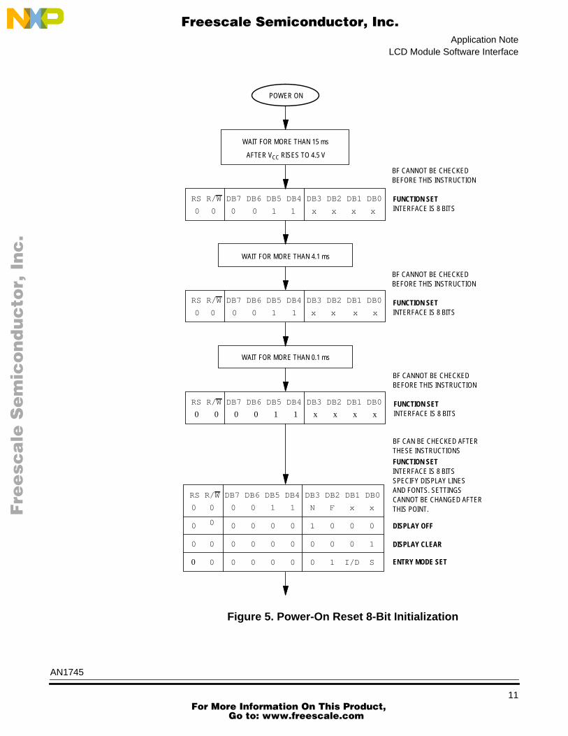
InitializationRoutines
To ensure proper initialization of the 207 module, a sequence ofinstruction codes must be executed. These instructions set the data buswidth, font type, and number of display lines. In addition, the LCD iscleared, and the entry mode for data is set.
Figure 5 shows the power-on reset initialization for an 8-bit data bus,while Figure 6 shows the power-on reset initialization for a 4-bit databus.
Table 5. LCD Address Map
Bit 1 Bit 2 Bit 3 Bit 4 Bit 5 ... Bit 16 ... Bit 39 Bit 40
$00 $01 $02 $03 $04 ... $0F ... $26 $27
$40 $41 $42 $43 $44 ... $4F ... $66 $67
AN1745
10 For More Information On This Product,
Go to: www.freescale.com
Application NoteLCD Module Software Interface
F
ree
sca
le S
em
ico
nd
uc
tor,
I
Freescale Semiconductor, Inc.n
c..
.
Figure 5. Power-On Reset 8-Bit Initialization
POWER ON
WAIT FOR MORE THAN 15 ms
AFTER VCC RISES TO 4.5 V
RS R/ W DB7 DB6 DB5 DB4 DB3 DB2 DB1 DB0
0 0 00 1 1 x x x x
RS R/ W DB7 DB6 DB5 DB4 DB3 DB2 DB1 DB0
0 0 00 1 1 x x x x
WAIT FOR MORE THAN 0.1 ms
RS R/ W DB7 DB6 DB5 DB4 DB3 DB2 DB1 DB0
0 0 00 1 1 x x x x
RS R/ W DB7 DB6 DB5 DB4 DB3 DB2 DB1 DB0
0 0 00 1 1 N F x x
0 0 00 0 0 1 0 0 0
0 0 00 0 0 0 0 0 1
0 0 00 0 0 0 1 I/D S
FUNCTION SET
BF CANNOT BE CHECKEDBEFORE THIS INSTRUCTION
INTERFACE IS 8 BITS
FUNCTION SET
BF CANNOT BE CHECKEDBEFORE THIS INSTRUCTION
INTERFACE IS 8 BITS
FUNCTION SET
BF CANNOT BE CHECKEDBEFORE THIS INSTRUCTION
INTERFACE IS 8 BITS
BF CAN BE CHECKED AFTERTHESE INSTRUCTIONS
FUNCTION SETINTERFACE IS 8 BITSSPECIFY DISPLAY LINESAND FONTS. SETTINGSCANNOT BE CHANGED AFTERTHIS POINT.
DISPLAY OFF
DISPLAY CLEAR
ENTRY MODE SET
WAIT FOR MORE THAN 4.1 ms
AN1745
11 For More Information On This Product,
Go to: www.freescale.com

Application Note
12
F
ree
sca
le S
em
ico
nd
uc
tor,
I
Freescale Semiconductor, Inc.n
c..
.
Figure 6. Power-On Reset 4-Bit Initialization
POWER ON
WAIT FOR MORE THAN 15 ms
AFTER VCC RISES TO 4.5 V
RS R/ W DB7 DB6 DB5 DB4
0 0 00 1 1
WAIT FOR MORE THAN 0.1 ms
RS R/ W DB7 DB6 DB5 DB4
0 0 00 1 0
0 0 FN X X
0 0 00 0 0
0 0 01 0 0
FUNCTION SET
BF CANNOT BE CHECKEDBEFORE THIS INSTRUCTION
INTERFACE IS 8 BITS
FUNCTION SET
BF CANNOT BE CHECKEDBEFORE THIS INSTRUCTION
INTERFACE IS 8 BITS
FUNCTION SET
BF CANNOT BE CHECKEDBEFORE THIS INSTRUCTION
INTERFACE IS 8 BITS
BF CAN BE CHECKED AFTERTHESE INSTRUCTIONS
FUNCTION SETINTERFACE IS 4 BITS
DISPLAY OFF
DISPLAY CLEAR
ENTRY MODE SET
WAIT FOR MORE THAN 4.1 ms
RS R/ W DB7 DB6 DB5 DB4
0 0 00 1 1
RS R/ W DB7 DB6 DB5 DB4
0 0 00 1 1
0 0 00 0 0
0 0 00 0 1
0 0 00 0 0
0 0 10 I/D S
0 0 00 1 0
FUNCTION SETINTERFACE IS 4 BITSSPECIFY DISPLAY LINES AND FONTS.SETTINGS CANNOT BE CHANGED.
AN1745
For More Information On This Product,
Go to: www.freescale.com

Application NoteMC68HC705C8A Interface
F
ree
sca
le S
em
ico
nd
uc
tor,
I
Freescale Semiconductor, Inc.n
c..
.
MC68HC705C8A Interface
Choosing between an 8- and a 4-bit data bus is usually defined by theI/O (input/output) and code space constraints of the application. Toanalyze both, two different test routines were written to demonstrate the8-bit and 4-bit bus configurations. Also, the R/W pin of the 207 wasgrounded for write executions only. Since we cannot check the BF flag,the delay times stated in Table 3 must be observed.
Although these routines were tested on an MC68HC705C8A device, anyHC05 device with enough memory and I/O can execute these routines.A simple change in the memory map should allow the code to be portedto other HC05s.
Hardware The code was tested on these development tools:
• M68MMPFB0508 — MMEVS platform board
• X68EM05C9A — C/D series emulation module
• M68CBL05B — Low noise flex cable
• M68TB05C9P40 — 40-pin PLCC target head adapter
The schematic shown in Figure 7 shows a typical circuit used tointerface the MC68HC705C8A to the 207.
AN1745
13 For More Information On This Product,
Go to: www.freescale.com

Application Note
F
ree
sca
le S
em
ico
nd
uc
tor,
I
Freescale Semiconductor, Inc.n
c..
.
Figure 7. Typical C8A-to-207 Circuit
Software The software written to demonstrate the MC68HC705C8A to LCDmodule interface is shown in the following appendices.
• Appendix A — Flowcharts
• Appendix B — 8-Bit Bus Code
• Appendix C — 4-Bit Bus Code
The flowchart roughly sketches out the routines. The code was writtento take pre-defined messages in ROM and easily display them by callinga subroutine. If the MC68HC705C8A is receiving messages from theSPI or SCI, put the message in a temporary RAM buffer and change themessage routine to start reading ASCII characters from the start of thebuffer.
LOW
VOLTAGE
DETECT
RESET
+5 V +5 V
VDD
IRQ
10 K
POT
+5 V
LCD MODULE
1
2
3
VCC
VSS
VEE
DB7 DB6 DB5 DB4 DB3 DB2 DB1 DB0
PB7
PB6
PB5
PB4
PB3
PB2
PB1
PB0
14 13 12 11 10 9 8 7
PA0
PA1
PA2
R/W
RS
E
5
4
6
4-MHz
CLOCK
CIRCUITRY
OSC1
OSC2
AN1745
14 For More Information On This Product,
Go to: www.freescale.com

Application NoteReferences
F
ree
sca
le S
em
ico
nd
uc
tor,
I
Freescale Semiconductor, Inc.n
c..
.
References
MC68HC705C8A Technical Data, Freescale order numberMC68HC705C8A/D, Freescale, 1996.
M68HC05 Applications Guide, Freescale order numberM68HC05AG/AD/D, Freescale, 1996.
DMC-16207 Digikey #73-1025-ND.
1997 Optrex LCD Databook Digikey #73-1001-ND.
AN1745
15 For More Information On This Product,
Go to: www.freescale.com

Application Note
F
ree
sca
le S
em
ico
nd
uc
tor,
I
Freescale Semiconductor, Inc.n
c..
.
Appendix A — Flowcharts
Figure 8. Main Flowchart
START
INITIALIZE PORT PINSWAIT FOR 15 ms
SEND FUNCTION CODE $38WAIT FOR 4.1 ms
SEND FUNCTION CODE $38WAIT FOR 0.1 ms
SEND FUNCTION CODE $38
FUNCTION CODE $388 BIT BUS, 2 ROWS, 5X7 DOTS
DISPLAY CODE $0CDISPLAY ON, CURSOR OFF, NO BLINKING
CLEAR DISPLAY CODE $01CLEAR DISPLAY, CURSOR AT ADDR $00
WAIT FOR 1.6 ms
ENTRY MODE CODE $06INCREMENT, NO DISPLAY SHIFT
JUMP SUB TO MESSAGE1
JUMP SUB TO MESSAGE2
INFINITE LOOP
JSR TO LCD_WRITE
JSR TO LCD_WRITE
JSR TO LCD_WRITE
JSR TO LCD_WRITE
AN1745
16 For More Information On This Product,
Go to: www.freescale.com

Application NoteAppendix A — Flowcharts
F
ree
sca
le S
em
ico
nd
uc
tor,
I
Freescale Semiconductor, Inc.n
c..
.
Figure 9. LCD_Write Subroutine Flowchart
Figure 10. LCD_ADDR Subroutine Flowchart
LCD_WRITE
STORE ACC TO LCD DATA PORT
CLOCK E
WAIT FOR 40 µs
RETURN FROM SUB
LCD_ADDR
STORE ACC TO LCD DATA PORT
CLOCK E
WAIT FOR 40 µs
RETURN FROM SUB
CLEAR RS, INSTRUCTION MODE
SET RS, INSTRUCTION MODE
AN1745
17 For More Information On This Product,
Go to: www.freescale.com

Application Note
F
ree
sca
le S
em
ico
nd
uc
tor,
I
Freescale Semiconductor, Inc.n
c..
.
Figure 11. Message Subroutine Flowchart
MESSAGE
LOAD ACC WITH LCD ADDRESS
JSR TO LCD_ADDR
CLEAR INDEX REGISTER
LOAD ACC FROM X POINTINGTO MESSAGE BUFFER
ACC = 0?
END OF BUFFER?
JSR TO LCD_WRITE
INCREMENT INDEX REGISTER
RETURN FROM SUB
YES
NO
AN1745
18 For More Information On This Product,
Go to: www.freescale.com

Application NoteAppendix B — 8-Bit Bus Code
F
ree
sca
le S
em
ico
nd
uc
tor,
I
Freescale Semiconductor, Inc.n
c..
.
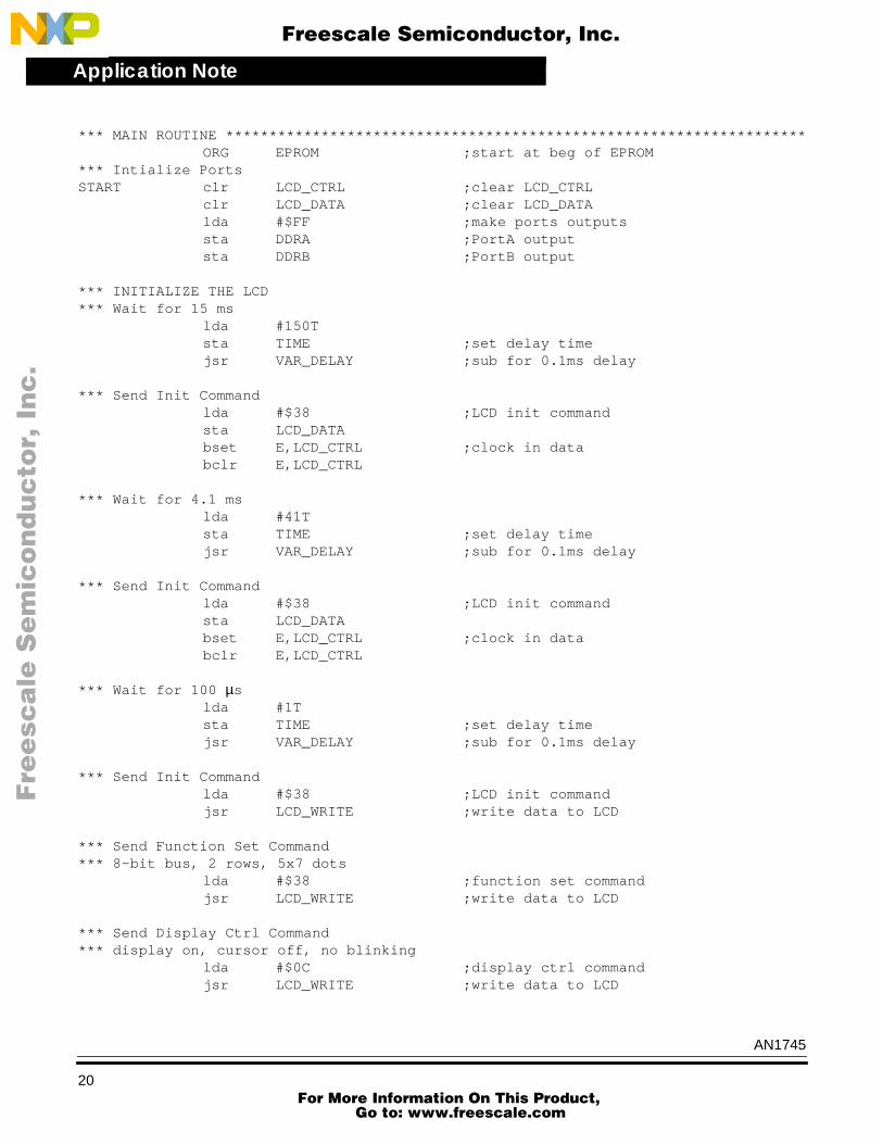
Appendix B — 8-Bit Bus Code
*************************************************************************************** File name: LCD_MOD8.ASM* Example Code for LCD Module (HD44780) using 8-bit bus* Ver: 1.0* Date: April 10, 1998* Author: Mark Glenewinkel* Field Applications* Consumer Systems Group* Assembler: P&E IDE ver 1.02** For code explanation and flowcharts, please consult Freescale Application Note* "Interfacing the HC705C8A to an LCD Module" Literature # AN1745/D*************************************************************************************
*** SYSTEM DEFINITIONS AND EQUATES ***************************************************** Internal Register DefinitionsPORTA EQU $00 ;LCD control signalsPORTB EQU $01 ;LCD data busDDRA EQU $04 ;data direction for PortADDRB EQU $05 ;data direction for PortB
*** Application Specific DefinitionsLCD_CTRL EQU $00 ;PORTALCD_DATA EQU $01 ;PORTBE EQU 0T ;PORTA, bit 0RW EQU 2T ;PORTA, bit 2RS EQU 1T ;PORTA, bit 1
*** Memory DefinitionsEPROM EQU $160 ;start of EPROM memRAM EQU $50 ;start of RAM memMSG_STORAGE EQU $500 ;start of message blockRESET EQU $1FFE ;vector for reset
*** RAM VARIABLES************************************************************************************
ORG RAMTIME DB 1 ;used for delay time
AN1745
19 For More Information On This Product,
Go to: www.freescale.com
Application Note
F
ree
sca
le S
em
ico
nd
uc
tor,
I
Freescale Semiconductor, Inc.n
c..
.
*** MAIN ROUTINE *******************************************************************ORG EPROM ;start at beg of EPROM
*** Intialize PortsSTART clr LCD_CTRL ;clear LCD_CTRL
clr LCD_DATA ;clear LCD_DATAlda #$FF ;make ports outputssta DDRA ;PortA outputsta DDRB ;PortB output
*** INITIALIZE THE LCD*** Wait for 15 ms
lda #150Tsta TIME ;set delay timejsr VAR_DELAY ;sub for 0.1ms delay
*** Send Init Commandlda #$38 ;LCD init commandsta LCD_DATAbset E,LCD_CTRL ;clock in databclr E,LCD_CTRL
*** Wait for 4.1 mslda #41Tsta TIME ;set delay timejsr VAR_DELAY ;sub for 0.1ms delay
*** Send Init Commandlda #$38 ;LCD init commandsta LCD_DATAbset E,LCD_CTRL ;clock in databclr E,LCD_CTRL
*** Wait for 100 µslda #1Tsta TIME ;set delay timejsr VAR_DELAY ;sub for 0.1ms delay
*** Send Init Commandlda #$38 ;LCD init commandjsr LCD_WRITE ;write data to LCD
*** Send Function Set Command*** 8-bit bus, 2 rows, 5x7 dots
lda #$38 ;function set commandjsr LCD_WRITE ;write data to LCD
*** Send Display Ctrl Command*** display on, cursor off, no blinking
lda #$0C ;display ctrl commandjsr LCD_WRITE ;write data to LCD
AN1745
20 For More Information On This Product,
Go to: www.freescale.com

Application NoteAppendix B — 8-Bit Bus Code
F
ree
sca
le S
em
ico
nd
uc
tor,
I
Freescale Semiconductor, Inc.n
c..
.
*** Send Clear Display Command*** clear display, cursor addr=0
lda #$01 ;clear display commandjsr LCD_WRITE ;write data to LCDlda #16Tsta TIME ;set delay time for 1.6 msjsr VAR_DELAY ;sub for 0.1ms delay
*** Send Entry Mode Command*** increment, no display shift
lda #$06 ;entry mode commandjsr LCD_WRITE ;write data to LCD
*** SEND MESSAGES*** Set the address, send data
jsr MESSAGE1 ;send Message1jsr MESSAGE2 ;send Message2
DUMMY bra DUMMY ;done with example
*** SUBROUTINES *********************************************************************** Routine creates a delay according to the formula*** TIME*100 µs using a 2-MHz internal bus*** Cycle count per instruction shownVAR_DELAY lda #33T ;2L1 deca ;3
bne L1 ;3dec TIME ;5bne VAR_DELAY ;3rts ;6
*** Routine sends LCD DataLCD_WRITE sta LCD_DATA
bset E,LCD_CTRL ;clock in databclr E,LCD_CTRLlda #13T ;2 40 µs delay for LCD
L2 deca ;3bne L2 ;3rts
*** Routine sends LCD AddressLCD_ADDR bclr RS,LCD_CTRL ;LCD in command mode
sta LCD_DATAbset E,LCD_CTRL ;clock in databclr E,LCD_CTRLlda #13T ;2 40 µs delay
L4 deca ;3bne L4 ;3bset RS,LCD_CTRL ;LCD in data moderts
AN1745
21 For More Information On This Product,
Go to: www.freescale.com

Application Note
F
ree
sca
le S
em
ico
nd
uc
tor,
I
Freescale Semiconductor, Inc.n
c..
.
MESSAGE1 lda #$84 ;addr = $04 jsr LCD_ADDR ;send addr to LCD
clrxL3 lda MSG1,X ;load AccA w/char from msg
beq OUTMSG1 ;end of msg?jsr LCD_WRITE ;write data to LCDincxbra L3 ;loop to finish msg
OUTMSG1 rts
MESSAGE2 lda #$C0 ;addr = $40jsr LCD_ADDR ;send addr to LCDclrx
L5 lda MSG2,X ;load AccA w/char from msgbeq OUTMSG2 ;end of msg?jsr LCD_WRITE ;write data to LCDincxbra L5 ;loop to finish msg
OUTMSG2 rts
*** MESSAGE STORAGE ****************************************************************ORG MSG_STORAGE
MSG1 db 'Freescale'db 0
MSG2 db 'Microcontrollers'db 0
*** VECTOR TABLE *******************************************************************ORG RESETDW START
AN1745
22 For More Information On This Product,
Go to: www.freescale.com

Application NoteAppendix C — 4-Bit Bus Code
F
ree
sca
le S
em
ico
nd
uc
tor,
I
Freescale Semiconductor, Inc.n
c..
.
Appendix C — 4-Bit Bus Code
************************************************************************************** File name: LCD_MOD4.ASM* Example Code for LCD Module (HD44780) using 4-bit bus* Ver: 1.0* Date: April 10, 1998* Author: Mark Glenewinkel* Freescale Field Applications* Consumer Systems Group* Assembler: P&E IDE ver 1.02** For code explanation and flowcharts, please consult Freescale Application Note* "Interfacing the HC705C8A to an LCD Module" Literature # AN1745/D*************************************************************************************
*** SYSTEM DEFINITIONS AND EQUATES ***************************************************** Internal Register DefinitionsPORTA EQU $00 ;LCD control signalsPORTB EQU $01 ;LCD data busDDRA EQU $04 ;data direction for PortADDRB EQU $05 ;data direction for PortB
*** Application Specific DefinitionsLCD_CTRL EQU $00 ;PORTALCD_DATA EQU $01 ;PORTBE EQU 0T ;PORTA, bit 0RW EQU 2T ;PORTA, bit 2RS EQU 1T ;PORTA, bit 1
*** Memory DefinitionsEPROM EQU $160 ;start of EPROM memRAM EQU $50 ;start of RAM memMSG_STORAGE EQU $500 ;start of message blockRESET EQU $1FFE ;vector for reset
*** RAM VARIABLES ******************************************************************ORG RAM
TIME DB 1 ;used for delay time
AN1745
23 For More Information On This Product,
Go to: www.freescale.com

Application Note
F
ree
sca
le S
em
ico
nd
uc
tor,
I
Freescale Semiconductor, Inc.n
c..
.
*** MAIN ROUTINE *******************************************************************ORG EPROM ;start at beg of EPROM
*** Intialize PortsSTART clr LCD_CTRL ;clear LCD_CTRL
clr LCD_DATA ;clear LCD_DATAlda #$FF ;make ports outputssta DDRA ;PortA outputsta DDRB ;PortB output
*** INITIALIZE THE LCD*** Wait for 15 ms
lda #150Tsta TIME ;set delay timejsr VAR_DELAY ;sub for 0.1ms delay
*** Send Init Commandlda #$30 ;LCD init commandsta LCD_DATAbset E,LCD_CTRL ;clock in databclr E,LCD_CTRL
*** Wait for 4.1 mslda #41Tsta TIME ;set delay timejsr VAR_DELAY ;sub for 0.1ms delay
*** Send Init Commandlda #$30 ;LCD init commandsta LCD_DATAbset E,LCD_CTRL ;clock in databclr E,LCD_CTRL
*** Wait for 100 µslda #1Tsta TIME ;set delay timejsr VAR_DELAY ;sub for 0.1ms delay
*** Send Init Commandlda #$30 ;LCD init commandjsr LCD_WRITE ;write data to LCD
*** Send Function Set Command*** 4-bit bus, 2 rows, 5x7 dots
lda #$20 ;function set commandjsr LCD_WRITE ;write data to LCDlda #$20 ;function set commandjsr LCD_WRITE ;write data to LCDlda #$80 ;function set commandjsr LCD_WRITE ;write data to LCD
AN1745
24 For More Information On This Product,
Go to: www.freescale.com

Application NoteAppendix C — 4-Bit Bus Code
F
ree
sca
le S
em
ico
nd
uc
tor,
I
Freescale Semiconductor, Inc.n
c..
.
*** Send Display Ctrl Command*** display on, cursor off, no blinking
lda #$00 ;display ctrl command MSBjsr LCD_WRITE ;write data to LCDlda #$C0 ;display ctrl command LSBjsr LCD_WRITE ;write data to LCD
*** Send Clear Display Command*** clear display, cursor addr=0
lda #$00 ;clear display command MSBjsr LCD_WRITE ;write data to LCDlda #16Tsta TIMEjsr VAR_DELAY ;delay for 1.6 mslda #$10 ;clear display command LSBjsr LCD_WRITE ;write data to LCDlda #16Tsta TIMEjsr VAR_DELAY ;delay for 1.6 ms
*** Send Entry Mode Command*** increment, no display shift
lda #$00 ;entry mode command MSBjsr LCD_WRITE ;write data to LCDlda #$60 ;entry mode command LSBjsr LCD_WRITE ;write data to LCD
*** SEND MESSAGES*** Set the address, send data
jsr MESSAGE1 ;send Message1jsr MESSAGE2 ;send Message2
DUMMY bra DUMMY ;done with example
*** SUBROUTINES *********************************************************************** Routine creates a delay according to the formula*** TIME*100 µs using a 2-MHz internal bus*** Cycle count per instruction shownVAR_DELAY lda #33T ;2L1 deca ;3
bne L1 ;3dec TIME ;5bne VAR_DELAY ;3rts ;6
AN1745
25 For More Information On This Product,
Go to: www.freescale.com

Application Note
F
ree
sca
le S
em
ico
nd
uc
tor,
I
Freescale Semiconductor, Inc.n
c..
.
*** Routine sends LCD DataLCD_WRITE sta LCD_DATA
bset E,LCD_CTRL ;clock in databclr E,LCD_CTRLlda #13T ;2 40 µs delay for LCD
L2 deca ;3bne L2 ;3rts
*** Routine sends LCD AddressLCD_ADDR bclr RS,LCD_CTRL ;LCD in command mode
sta LCD_DATAbset E,LCD_CTRL ;clock in databclr E,LCD_CTRLlda #13T ;2 40 µs delay
L4 deca ;3bne L4 ;3bset RS,LCD_CTRL ;LCD in data moderts
MESSAGE1 lda #$80 ;addr = $04 MSBjsr LCD_ADDR ;send addr to LCDlda #$40 ;addr = $04 LSBjsr LCD_ADDR ;send addr to LCDclrx
L3 lda MSG1,X ;load AccA w/char from msgbeq OUTMSG1 ;end of msg?jsr LCD_WRITE ;write data to LCDlda MSG1,X ;load Acca w/char from msgasla ;shift LSB to MSBaslaaslaaslajsr LCD_WRITE ;write data to LCDincxbra L3 ;loop to finish msg
OUTMSG1 rts
MESSAGE2 lda #$C0 ;addr = $40 MSBjsr LCD_ADDR ;send addr to LCDlda #$00 ;addr = $40 LSBjsr LCD_ADDR ;send addr to LCDclrx
L5 lda MSG2,X ;load Acca w/char from msgbeq OUTMSG2 ;end of msg?jsr LCD_WRITE ;write data to LCDlda MSG2,X ;load AccA w/char from msgasla ;shift LSB to MSBaslaasla
asla
AN1745
26 For More Information On This Product,
Go to: www.freescale.com

Application NoteAppendix C — 4-Bit Bus Code
F
ree
sca
le S
em
ico
nd
uc
tor,
I
Freescale Semiconductor, Inc.n
c..
.
jsr LCD_WRITE ;write data to LCDincxbra L5 ;loop to finish msg
OUTMSG2 rts
*** MESSAGE STORAGE ****************************************************************ORG MSG_STORAGE
MSG1 db 'Freescale'db 0
MSG2 db 'Microcontrollers'db 0
*** VECTOR TABLE *******************************************************************ORG RESETDW START
AN1745
27 For More Information On This Product,
Go to: www.freescale.com

N
ON
-D
IS
CL
OS
UR
E
AG
RE
EM
EN
T
RE
QU
IR
ED
Application Note
F
ree
sca
le S
em
ico
nd
uc
tor,
I
Freescale Semiconductor, Inc.n
c..
.
AN1745/D For More Information On This Product,
Go to: www.freescale.com