Embed Size (px)
Citation preview

Application ReportSPRAA52 − August 2004
1
Interfacing a CMOS Sensor to the TMS320DM642 UsingRaw Capture Mode
Miguel Hernandez IV Device Applications
ABSTRACT
This document contains information on how to interface the TMS320DM642 to a CMOSDigital Image Sensor in raw capture mode. A complete example is shown, including hardwareand software interfaces. The software consists of a set of routines that are compatible withthe Video Port Mini-Driver and External Device Control interface. The discussed interface isproven and has been tested from 320x240 at 120 frames per second to 1920x1080 at 19frames per second. This document is accompanied by example software designed to operatewith the TMS320DM642 EVM and is available electronically from the TI website.
Contents
1 Introduction 2 . . . . . . . . . . . . . . . . . . . . . . . . . . . . . . . . . . . . . . . . . . . . . . . . . . . . . . . . . . . . . . . . . . . . . . . .
2 CMOS Digital Image Sensor Overview 3 . . . . . . . . . . . . . . . . . . . . . . . . . . . . . . . . . . . . . . . . . . . . . . . . 2.1 CMOS Sensor Signal Descriptions 3 . . . . . . . . . . . . . . . . . . . . . . . . . . . . . . . . . . . . . . . . . . . . . . . . . 2.2 CMOS Sensor Register Descriptions 4 . . . . . . . . . . . . . . . . . . . . . . . . . . . . . . . . . . . . . . . . . . . . . . .
2.2.1 Row and Column Size 5 . . . . . . . . . . . . . . . . . . . . . . . . . . . . . . . . . . . . . . . . . . . . . . . . . . . . . 2.2.2 Horizontal and Vertical Blanking 5 . . . . . . . . . . . . . . . . . . . . . . . . . . . . . . . . . . . . . . . . . . . . . 2.2.3 Shutter Width 5 . . . . . . . . . . . . . . . . . . . . . . . . . . . . . . . . . . . . . . . . . . . . . . . . . . . . . . . . . . . . . 2.2.4 Pixel Clock Control 5 . . . . . . . . . . . . . . . . . . . . . . . . . . . . . . . . . . . . . . . . . . . . . . . . . . . . . . . . 2.2.5 Read Mode 1 5 . . . . . . . . . . . . . . . . . . . . . . . . . . . . . . . . . . . . . . . . . . . . . . . . . . . . . . . . . . . . . 2.2.6 Read Mode 2 5 . . . . . . . . . . . . . . . . . . . . . . . . . . . . . . . . . . . . . . . . . . . . . . . . . . . . . . . . . . . . .
2.3 Reading and Writing the CMOS Sensor Registers 6 . . . . . . . . . . . . . . . . . . . . . . . . . . . . . . . . . . . 2.3.1 Sensor Output Data Format 7 . . . . . . . . . . . . . . . . . . . . . . . . . . . . . . . . . . . . . . . . . . . . . . . .
3 DM642 Video Port Overview 7 . . . . . . . . . . . . . . . . . . . . . . . . . . . . . . . . . . . . . . . . . . . . . . . . . . . . . . . . . 3.1 Video Capture Port Signal Descriptions 8 . . . . . . . . . . . . . . . . . . . . . . . . . . . . . . . . . . . . . . . . . . . . . 3.2 Raw Capture Mode 8 . . . . . . . . . . . . . . . . . . . . . . . . . . . . . . . . . . . . . . . . . . . . . . . . . . . . . . . . . . . . . . 3.3 Frame Synchronization 9 . . . . . . . . . . . . . . . . . . . . . . . . . . . . . . . . . . . . . . . . . . . . . . . . . . . . . . . . . . .
4 Sensor Interface to the to DM642 10 . . . . . . . . . . . . . . . . . . . . . . . . . . . . . . . . . . . . . . . . . . . . . . . . . . . 4.1 Hardware Interface 10 . . . . . . . . . . . . . . . . . . . . . . . . . . . . . . . . . . . . . . . . . . . . . . . . . . . . . . . . . . . . . 4.2 Software Interface 12 . . . . . . . . . . . . . . . . . . . . . . . . . . . . . . . . . . . . . . . . . . . . . . . . . . . . . . . . . . . . . .
4.2.1 Raw Capture Mode Initialization 12 . . . . . . . . . . . . . . . . . . . . . . . . . . . . . . . . . . . . . . . . . . . 4.2.2 Raw Display Mode Initialization 15 . . . . . . . . . . . . . . . . . . . . . . . . . . . . . . . . . . . . . . . . . . . . 4.2.3 Sensor EDC 17 . . . . . . . . . . . . . . . . . . . . . . . . . . . . . . . . . . . . . . . . . . . . . . . . . . . . . . . . . . . . .
4.3 Capture and Display Performance 18 . . . . . . . . . . . . . . . . . . . . . . . . . . . . . . . . . . . . . . . . . . . . . . . .
5 Conclusion 18 . . . . . . . . . . . . . . . . . . . . . . . . . . . . . . . . . . . . . . . . . . . . . . . . . . . . . . . . . . . . . . . . . . . . . . . .
6 References 19 . . . . . . . . . . . . . . . . . . . . . . . . . . . . . . . . . . . . . . . . . . . . . . . . . . . . . . . . . . . . . . . . . . . . . . . .
Trademarks are the property of their respective owners.

SPRAA52
2 Interfacing a CMOS Sensor to the TMS320DM642 Using Raw Capture Mode
Appendix A Sensor Daughter Card Schematics for the DM642 EVM 20 . . . . . . . . . . . . . . . . . . . . . .
List of Figures
Figure 1. Non-Continuous and Continuous LINE_VALID Formats 6 . . . . . . . . . . . . . . . . . . . . . . . . . . . . . . Figure 2. I2C Write to Column Size Register (0x04) with the Value 0x027F 6 . . . . . . . . . . . . . . . . . . . . . . Figure 3. I2C Read from Column Size Register (0x04). 0x027F Returned 7 . . . . . . . . . . . . . . . . . . . . . . . Figure 4. Bayer Color Pattern 7 . . . . . . . . . . . . . . . . . . . . . . . . . . . . . . . . . . . . . . . . . . . . . . . . . . . . . . . . . . . . . Figure 5. VCxSTRT1 Register 9 . . . . . . . . . . . . . . . . . . . . . . . . . . . . . . . . . . . . . . . . . . . . . . . . . . . . . . . . . . . . . Figure 6. Initializing VCVBLNKP 10 . . . . . . . . . . . . . . . . . . . . . . . . . . . . . . . . . . . . . . . . . . . . . . . . . . . . . . . . . . Figure 7. Sensor Interface to the DM642 11 . . . . . . . . . . . . . . . . . . . . . . . . . . . . . . . . . . . . . . . . . . . . . . . . . . . Figure 8. Proper LINE_VALID Operation 12 . . . . . . . . . . . . . . . . . . . . . . . . . . . . . . . . . . . . . . . . . . . . . . . . . . . Figure 9. Capture Configuration Structure 13 . . . . . . . . . . . . . . . . . . . . . . . . . . . . . . . . . . . . . . . . . . . . . . . . . . Figure 10. Raw Capture Mode Configuration 14 . . . . . . . . . . . . . . . . . . . . . . . . . . . . . . . . . . . . . . . . . . . . . . . Figure 11. SAA7105 Configuration for SVGA Display 16 . . . . . . . . . . . . . . . . . . . . . . . . . . . . . . . . . . . . . . . . Figure 12. RGB565 Data Format 16 . . . . . . . . . . . . . . . . . . . . . . . . . . . . . . . . . . . . . . . . . . . . . . . . . . . . . . . . . Figure 13. Bayer Pattern (4x4) 17 . . . . . . . . . . . . . . . . . . . . . . . . . . . . . . . . . . . . . . . . . . . . . . . . . . . . . . . . . . . Figure 14. FVID Object Initialization 17 . . . . . . . . . . . . . . . . . . . . . . . . . . . . . . . . . . . . . . . . . . . . . . . . . . . . . . .
List of Tables
Table 1 Sensor Signal Descriptions 4. . . . . . . . . . . . . . . . . . . . . . . . . . . . . . . . . . . . . . . . . . . . . . . . . . . . . Table 2 I2C Sensor Addresses 6. . . . . . . . . . . . . . . . . . . . . . . . . . . . . . . . . . . . . . . . . . . . . . . . . . . . . . . . . Table 3 Video Capture Port Signal Descriptions (Raw Capture Mode) 8. . . . . . . . . . . . . . . . . . . . . . . Table 4 VCxSTOP1 Register Initialization 9. . . . . . . . . . . . . . . . . . . . . . . . . . . . . . . . . . . . . . . . . . . . . . . Table 5 VCxSTRT1 Bit Field Descriptions 9. . . . . . . . . . . . . . . . . . . . . . . . . . . . . . . . . . . . . . . . . . . . . . . Table 6 Capture and Display Performance 18. . . . . . . . . . . . . . . . . . . . . . . . . . . . . . . . . . . . . . . . . . . . . .
1 Introduction
Digital signal processors (DSPs) have become increasingly important in a wide range of videoand imaging applications, such as machine vision, medical imaging, security monitoring, digitalcameras and printers, and a large number of consumer applications driven by digital videoprocessing including DVDs, digital TV, and video telephony. These applications arecharacterized by requirements for processing flexibility, sophisticated algorithms, and high datarates. The DM642 is a DSP designed to handle the computational requirements of the aboveapplications.
The Texas Instruments DM642 has three 20-bit video ports that can be configured for differentvideo standards, such as BT.656 or, as in the application this document describes, can be usedin raw data capture mode. The video ports are capable of driving encoders for display purposes,or they can capture data from various decoders and video sources. In the application describedby this document, the video source will be an MT9T001 CMOS Digital Image Sensor byMicron� Technology, Inc. This application is applicable to other sensors and video A/Dconverters having similar interfaces.

SPRAA52
3 Interfacing a CMOS Sensor to the TMS320DM642 Using Raw Capture Mode
The following sections give an overview of the MT9T001 and DM642 video port configured forraw capture mode operation. These sections describe the physical and logical interfaces, andprovide a sample application proving the discussed system.
2 CMOS Digital Image Sensor Overview
The CMOS Digital Image Sensor used in this document is the MT9T001 by Micron�Technology, Inc. and will be hereafter referred to as the Sensor. The Sensor is a QXGA-formatdigital image device with an active imaging pixel array of 2048x1536. The Sensor provides acolor resolution of 10 bits per pixel, is able to capture both continuous video and single framesprogressively, and is programmable through an I2C serial interface. The following sectionsprovide an overview of the Sensor and describe the physical and logical interfaces in the contextof a Sensor to DM642 interface in raw capture mode.
2.1 CMOS Sensor Signal Descriptions
The following table lists and describes the Sensor input/output (I/O) signals as they pertain tothe Sensor to DM642 interface in raw capture mode. Signals generated by the DM642 areinputs; signals generated by the Sensor are outputs; and bidirectional signals are I/O. Note thatsome Sensor signals are not used and not discussed. For a full signal description, refer toMicron’s Data Sheet �.

SPRAA52
4 Interfacing a CMOS Sensor to the TMS320DM642 Using Raw Capture Mode
Table 1. Sensor Signal Descriptions
Signal
Symbol Name I/O Description
VAAPIX Analog pixel power − Power supply for pixel array, 3.3V
VDD Digital power supply − Power supply for digital block, 3.3V
DGND Digital ground − Isolated ground for digital block.
VAA Analog power supply − Power supply for analog block, 3.3V
AGND Analog ground − Isolated ground for analog block and pixel array.
DOUT[9:0] Data out O Pixel data output
PIXCLK Pixel clock O Pixel data outputs are valid during the falling/rising edge of thisclock. See the Pixel Clock Control register for options. The fre-quency is equal to that of Master Clock In.
LINE_VALID Output line valid O This output is high whenever a line of valid pixel data is availableon the data bus (see Read Mode 2 register for options).
FRAME_VALID Output frame valid O Not used and left unconnected.
SDATA I2C data bus I/O I2C data bus
SCLK I2C clock I I2C clock
/RESET† Reset I All registers assume factory defaults
/OE Output enable I Enables outputs when active. Tied to ground.
CLK_IN Master clock in I Master clock into Sensor (48 MHz maximum).
GSHT_CTL Global shutter control I Not used and left unconnected.
STROBE Output strobe O Not used and left unconnected.
STANDBY Standby I Not used and tied to ground.
TRIGGER Trigger I Not used and left unconnected.
NC No connect − These pins must be left unconnected.
† ‘/’ prefix denotes low active signal
2.2 CMOS Sensor Register Descriptions
The Sensor is programmed through registers via the I2C serial interface. Each register addressconsists of 8 bits, while register data consists of 16 bits. This section only describes thoseregisters necessary for operation in the context of the Sensor to DM642 interface in raw capturemode. All registers not discussed are operated according to default values, i.e. those valuesassigned to the registers at reset. For a full register description, see Micron’s Data Sheet � .

SPRAA52
5 Interfacing a CMOS Sensor to the TMS320DM642 Using Raw Capture Mode
2.2.1 Row and Column Size
These registers control the horizontal and vertical resolution of data to be captured by theSensor. The Sensor is capable of capturing a maximum resolution of 2048x1536, a minimumresolution of 2x2, and all resolutions in between. The values to be programmed in theseregisters are the desired resolution minus one (desired – 1), and must be an odd number. Forexample, if a resolution of 640x480 is desired, 639 and 479 must be programmed in the Columnand Row Size registers respectively.
2.2.2 Horizontal and Vertical Blanking
These registers control the blanking time in a row and between frames. Horizontal blanking isdefined in terms of pixel clocks (PIXCLK) and vertical blanking is defined in terms of row readouttimes.
2.2.3 Shutter Width
This register specifies the number of rows of integration and exposure time. The integration timeof the pixel is the amount of time the pixels are set to collect charge generated from light. SeeMicron’s Data Sheet � for formulas that govern the exposure time.
2.2.4 Pixel Clock Control
This register specifies the operation of the PIXCLK clock output, and consists of three fields:Invert Pixel Clock, Shift Pixel Clock, and Divide Pixel Clock. The field of interest for the Sensorto DM642 interface is the Invert Pixel Clock field. The LINE_VALID, FRAME_VALID, andDOUT[9:0] lines are synchronized with the PIXCLK output. This field determines whether theabove lines are synchronized to the rising or falling edge of PIXCLK. For the Sensor to DM642interface discussed in this document, the above lines must be set to the rising edge of PIXCLK.All other fields operate according to their default values.
2.2.5 Read Mode 1
This register specifies the capture operation of the Sensor, and consists of four fields: SnapshotMode, Strobe Enable, Strobe Width, and Strobe Override. The field of interest for the Sensor toDM642 interface is the Snapshot Mode field. This field determines whether the Sensor capturesdata continuously (video), or on a frame basis (pictures). For the Sensor to DM642 interfacediscussed in this document, the Sensor is set to operate continuously. All other fields operateaccording to their default values.
2.2.6 Read Mode 2
This register specifies the operation of the LINE_VALID signal with respect to theFRAME_VALID signal, and consists of three fields: No Bad Frames, Continuous LINE_VALID,and XOR LINE_VALID. The field of interest for the Sensor to DM642 interface is the ContinuousLINE_VALID field. This field determines whether the LINE_VALID signal is output during avertical blanking period or not. The figure below illustrates the LINE_VALID operation whenreading out four rows of valid data and three vertical blanking rows. The period during which theFRAME_VALID signal is low denotes a vertical blanking period. The LINE_VALID_0 andLINE_VALID_1 signals below represent the cases when the bit field in question is cleared andset respectively. For frame synchronization purposes (which will be discussed later in thisdocument), the LINE_VALID_0 signal is desired. All other bit fields in this register operateaccording to their default values.

SPRAA52
6 Interfacing a CMOS Sensor to the TMS320DM642 Using Raw Capture Mode
FRAME_VALID
LINE_VALID_0
LINE_VALID_1
Figure 1. Non-Continuous and Continuous LINE_VALID Formats
2.3 Reading and Writing the CMOS Sensor Registers
All Sensor registers are written and read through the I2C serial interface. The I2C address of theSensor is fixed and consists of seven bits of address and 1-bit of read/write direction. The tablebelow shows the read and write addresses of the Sensor.
Table 2. I2C Sensor Addresses
7 Address Bits (binary) Direction Mode Final Address (hex)
1011 101 1 Read 0xBB
1011 101 0 Write 0xBA
The Sensor data registers are 16 bits wide, so two 8-bit transfers are required when reading orwriting a register. A typical write sequence for writing 16 bits to a register is shown in the figurebelow. The sequence begins with a Start bit followed by the Sensor write address. After theSensor acknowledges the write address (A), a specific register address is issued, which is theColumn Size register in this example. At this point, the Sensor expects to receive two 8-bit datatransfers (0x02 and 0x7F) to complete the write process.
1 0 1 1 1 0 1 0 A 0 0 00 0 1 0 0 A 0 0 0 0 0 1 00 A 0 1 1 11 11 1 A
Sensor writeaddress
0x04register address
0x028 bit data
0x7F8 bit data
SCLK
SDATA
Figure 2. I2C Write to Column Size Register (0x04) with the Value 0x027F
The figure below shows a typical read sequence for reading 16 bits from a register. Thesequence begins with a Start bit followed by the Sensor write address. After the Sensoracknowledges the write address, a specific register address is issued (Column Size register). AStart bit is generated again and the Sensor read address is issued. At this point, the Sensor willtransmit two 8-bit data packets, and the read process ends with a No Acknowledge (N) followedby a Stop bit.

SPRAA52
7 Interfacing a CMOS Sensor to the TMS320DM642 Using Raw Capture Mode
1 0 1 1 1 0 1 0 A 0 0 00 0 1 0 0 A 1 0 1 1 0 11 1 A 1
SCLK
SDATA 00000 0 0 A 0 1 1 1 111 1 N
0xBAsensor write
address
0x04register address sensor read
address
0xBB 0x028 bit data
0x7F8 bit data
Figure 3. I2C Read from Column Size Register (0x04). 0x027F Returned
2.3.1 Sensor Output Data Format
The Sensor captures and outputs information in a Bayer color pattern as shown in the followingfigure which represents a 6x6 captured image. The odd rows are comprised of alternating greenand red pixels, and the even rows are comprised of alternating blue and green pixels.Alternatively, the color pattern can be viewed as the even columns made up of alternating greenand blue pixels, and the odd columns made up of alternating red and green pixels. Note that thecaptured image has twice as many green pixels as it does red and blue. Depending on theapplication, the Bayer color pattern may have to be converted to another format. As will beshown later in this document, the Bayer color pattern must be converted to RGB565 for displayon a monitor.
G R G R G R
B G B G B G
G R G R G R
B G B G B G
G R G R G R
B G B G B G
Figure 4. Bayer Color Pattern
3 DM642 Video Port Overview
The Texas Instruments DM642 has three 20-bit video ports that can be configured for differentvideo standards, such as BT.656, or, as in the application this document describes, can be usedin raw data capture mode. The video ports are capable of driving encoders for display purposes,or they can capture data from various decoders and video sources. The application described inthis document uses a Sensor as the video source. The following sections provide an overview ofthe video capture port configured for raw capture mode operation and describe the physical andlogical interfaces in the context of a Sensor to DM642 interface. For a full description of theDM642 video port and raw capture mode operation, refer to the TMS320C64x DSP VideoPort/VCXO Interpolated Control (VIC) Port Reference Guide (SPRU629) and theTMS320DM642 Video/Imaging Fixed-Point Digital Signal Processor Data Manual (SPRS200).

SPRAA52
8 Interfacing a CMOS Sensor to the TMS320DM642 Using Raw Capture Mode
3.1 Video Capture Port Signal Descriptions
The following table lists and describes the video capture port input/output (I/O) signals as theypertain to the Sensor to DM642 interface in raw capture mode. Signals generated by the DM642are outputs, signals generated by the Sensor are inputs, and bi-directional signals are I/O. Notethat some video port signals are not used and not discussed. For a full signal description, referto the TMS320C64x DSP Video Port/VCXO Interpolated Control (VIC) Port Reference Guide(SPRU629) and the TMS320DM642 Video/Imaging Fixed-Point Digital Signal Processor DataManual (SPRS200).
Table 3. Video Capture Port Signal Descriptions (Raw Capture Mode)
Video Port SignalUsage in RawCapture Mode I/O Description
VPxCLK0† VCLKINA I Video port clock line.
VPxCLK1 VCLKINB I Not Used.
VPxCTL0 CAPENA I Data capture enable. Data is sampled by the video port when this line is active.
VPxCTL1 CAPENB I Not Used.
VPxCTL2 FID I Not Used.
VPxD[9:0] − I Pixel data input lines.
VPxD[19:10] − I Not Used.
SCL‡ − O I2C clock.
SDA‡ − I/O I2C data line.
† ‘x’ is a general place holder that can represent video port 0, 1, or 2.‡ Not part of the video port, but used in the Sensor to DM642 interface.
3.2 Raw Capture Mode
In order to capture video from the Sensor, the DM642 video port must be configured to operatein raw capture mode. When operating in raw capture mode, no data selection or datainterpretation is performed by the DM642. This mode of operation is useful for video datacapture from a variety of A/D converters, such as the Sensor described in this document.
While operating in raw capture mode, the DM642 video port supports 8, 10, 16, and 20-bit dataword sizes. The 16 and 20-bit raw capture modes are designed to accept data from highresolution A/D converters, such as those used in medical imaging. The Sensor to DM642interface described in this document can function in both 8 and 10-bit resolutions.
In raw capture mode, the VPxD data lines are sampled by the interface when the CAPEN signalis active. Data is captured at the rate of the clock of the data source. The captured data set sizeis set by the VCXSTOP and VCYSTOP bit fields in the Video Capture Channel x Field 1 StopRegister (VCxSTOP1). When combined, the VCXSTOP and VCYSTOP fields allow the DM642to capture up to 224 data samples (VCXSTOP sets the lower 12 bits and VCYSTOP sets theupper 12 bits). Capture is complete when the captured data size reaches the combinedVCXSTOP and VCYSTOP value. Note that the CAPEN signal must remain inactive for aminimum of two cycles after the VCXSTOP and VCYSTOP counters have expired for properoperation. The table below demonstrates how to initialize the VCxSTOP1 register based on aframe size of 640x480.
SPRAA52
9 Interfacing a CMOS Sensor to the TMS320DM642 Using Raw Capture Mode
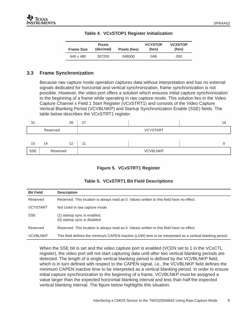
Table 4. VCxSTOP1 Register Initialization
Frame SizePixels
(decimal) Pixels (hex)VCYSTOP
(hex)VCXSTOP
(hex)
640 x 480 307200 04B000 04B 000
3.3 Frame Synchronization
Because raw capture mode operation captures data without interpretation and has no externalsignals dedicated for horizontal and vertical synchronization, frame synchronization is notpossible. However, the video port offers a solution which ensures initial capture synchronizationto the beginning of a frame while operating in raw capture mode. This solution lies in the VideoCapture Channel x Field 1 Start Register (VCxSTRT1) and consists of the Video CaptureVertical Blanking Period (VCVBLNKP) and Startup Synchronization Enable (SSE) fields. Thetable below describes the VCxSTRT1 register.
31 28 27 16
Reserved VCYSTART
15 14 12 11 0
SSE Reserved VCVBLNKP
Figure 5. VCxSTRT1 Register
Table 5. VCxSTRT1 Bit Field Descriptions
Bit Field Description
Reserved Reserved. This location is always read as 0. Values written to this field have no effect.
VCYSTART Not Used in raw capture mode.
SSE (1) startup sync is enabled.(0) startup sync is disabled
Reserved Reserved. This location is always read as 0. Values written to this field have no effect.
VCVBLNKP This field defines the minimum CAPEN inactive (LOW) time to be interpreted as a vertical blanking period.
When the SSE bit is set and the video capture port is enabled (VCEN set to 1 in the VCxCTLregister), the video port will not start capturing data until after two vertical blanking periods aredetected. The length of a single vertical blanking period is defined by the VCVBLNKP field,which is in turn defined with respect to the CAPEN signal, i.e., the VCVBLNKP field defines theminimum CAPEN inactive time to be interpreted as a vertical blanking period. In order to ensureinitial capture synchronization to the beginning of a frame, VCVBLNKP must be assigned avalue larger than the expected horizontal blanking interval and less than half the expectedvertical blanking interval. The figure below highlights this situation.

SPRAA52
10 Interfacing a CMOS Sensor to the TMS320DM642 Using Raw Capture Mode
HV
H
VCVBLNKP
VCVBLNKP
CAPEN
H = Horizontal blanking interval
V = Vertical blanking interval
Figure 6. Initializing VCVBLNKP
WARNING:Frame synchronization is only performed ONCE every time the video capture port isenabled (VCEN = 1). A noisy CAPEN signal may cause a loss of frame synchronization.To re-synchronize, the video port must be disabled, then re-enabled.
The method required to setup and operate the video port in raw capture mode will be discussedlater in this document.
4 Sensor Interface to the to DM642
There are many ways to interface the Sensor to the DM642 EVM in raw capture mode. Thissection describes one such implementation of this interface. A complete example is shown,including both hardware and software. The software is designed to operate with the Video PortMini-Driver for the DM642 EVM and is fully compliant with the External Device Control interface(EDC). For more information on the Video Port Mini-Driver and EDC, refer to the applicationreport The TMS320DM642 Video Port Mini−Driver (SPRA918).
4.1 Hardware Interface
The Sensor can be easily interfaced to the DM642 through the video port. A high level view ofthis interface is shown in the figure below. This interface is designed for video port channel Aoperation only. Note that some signals are not used and left unconnected.

SPRAA52
11 Interfacing a CMOS Sensor to the TMS320DM642 Using Raw Capture Mode
CLK_IN
PIXCLK
LINE_VALID
D[9:0]
SCLK
SDATA
TRIGGER
GSHT_CTL
FRAME_VALID
STROBE
RESET
STANDBY
OE
VCLKINA [VPxCLK0]
CAPENA [VPxCTL0]
VPxD[9:0]
SCL
SDA
VCLKINB [VPxCLK1]
CAPENB [VPxCTL1]
FID [VPxCTL2]
VPxD[19:10]
48 MHz
SYS_RESET
GND
Sensor DM642 EVM
NOTE: /SYS_RESET is connected to the RESET switch on the DM642 EVM.
Figure 7. Sensor Interface to the DM642
The FRAME_VALID signal on the Sensor is left unconnected because no input exists on theDM642 which can take advantage of this signal. However, the FRAME_VALID line is not neededsince the information necessary for proper operation with the DM642 is carried on theLINE_VALID signal. Recall that the LINE_VALID and FRAME_VALID signals indicate that a lineand frame of valid pixel data is available on the data bus. Because the DM642 samples datawhen CAPEN is active, proper video port and Sensor operation requires that the LINE_VALIDsignal be connected to the CAPEN signal.
The software interface must ensure that the LINE_VALID signal operates according to thenon-continuous format. Recall that the Read Mode 2 Sensor register can be configured fordifferent LINE_VALID formats based on the desired vertical blanking operation. For properoperation, the Read Mode 2 register must be programmed to ensure that the LINE_VALID signalis inactive during vertical blanking intervals. The figure below illustrates this operation.

SPRAA52
12 Interfacing a CMOS Sensor to the TMS320DM642 Using Raw Capture Mode
H
V
FRAME_VALID
LINE_VALID
H = Horizontal blankingV = Vertical blanking
Figure 8. Proper LINE_VALID Operation
In the Sensor to DM642 interface described above, the TRIGGER, STROBE, and GSHT_CTLsignals are not used and left unconnected. In an advanced design, these signals can be used toenable Snapshot Mode operation. In this mode, the TRIGGER signal can be connected to aGPIO on the DM642 and used to initiate the start of a single frame capture, STROBE can beused to turn on a flash, and GSHT_CTL can be combined with a mechanical shutter to achievesimultaneous exposure of all rows in the image. For more information on Snapshot Mode, referto Micron’s Data Sheet �.
4.2 Software Interface
The software interface performs the functions required to capture and display information fromthe Sensor, is designed to operate with the Video Port Mini-Driver for the DM642 EVM and isfully compliant with the EDC interface. The Mini-Driver consists of a generic portion whichconfigures both the video port and EDMA for data capture and display, and a board-specific part(EDC) which configures both the Sensor and SAA7105 video encoder for data capture anddisplay respectively. The following section describes the software used for data capture anddisplay from the Sensor. For more information on the Video Port Mini-Driver and EDC, refer tothe application report The TMS320DM642 Video Port Mini-Driver (SPRA918).
4.2.1 Raw Capture Mode Initialization
In order to initialize the video port in raw capture mode, the generic portion of the Mini-Driverhad to be modified. As of the writing of this document, the Video Port Mini-Driver does notsupport raw capture mode. The modified Video Port Mini-Driver with raw capture mode supportis included with the software that accompanies this document. This section describes themodified Mini-Driver and outlines the steps necessary to initialize the video port for raw capturemode.
Three files were modified to enable raw capture mode operation: _vport.h, vportcap.h, andvportcap.c (renamed to vportcap_RAW_support.c). These modified files are available fordownload with this document. The modified capture configuration structure is shown in the codesegment below.

SPRAA52
13 Interfacing a CMOS Sensor to the TMS320DM642 Using Raw Capture Mode
typedef struct { Int cmode; Int fldOp; Int scale; Int resmpl; Int bpk10Bit; Int hCtRst; Int vCtRst; Int fldDect; Int extCtl; Int fldInv; /* RAW CAPTURE INITIALIZATION SPECIFIC Modify structure to accept Raw Capture mode specific parameters for SSE Enable/Disable and VCVBLNKP. */ Uint16 sse; /* startup synchronization enable */ Uint16 vcvblnkp; /* minimum CAPEN inactive time to be interpreted as a vertical blanking period */ Uint16 fldXStrt1; Uint16 fldYStrt1; Uint16 fldXStrt2; Uint16 fldYStrt2; Uint16 fldXStop1; Uint16 fldYStop1; Uint16 fldXStop2; Uint16 fldYStop2; Uint16 thrld; Int numFrmBufs; Int alignment; Int mergeFlds; Int segId; Int edmaPri; Int irqId;} VPORTCAP_Params;
Figure 9. Capture Configuration Structure
Two parameters (Uint16 sse and Uint16 vcvblnkp) were added to the configuration structure toensure that the SSE and VCVBLNKP fields in the VCxSTRT1 register (described in a previoussection) are correctly programmed. All other parameters in the configuration structure areunmodified and are described in the application report TMS320DM642 Video Port Mini-Driver(SPRA918). The following are possible settings for the ‘sse’ and ‘vcbblnkp’ parameters.
� sse: enables or disables startup synchronization
− VPORTCAP_SSE_ENABLE
− VPORTCAP_SSE_DISABLE
� vcvblnkp: specifies the minimum CAPEN inactive time to be interpreted as a verticalblanking period.
− Any value between 0 and 0xFFF
The code segment below shows the capture configuration structure initialized to enable 8-bit rawcapture mode (progressive) for a resolution of 640x480.

SPRAA52
14 Interfacing a CMOS Sensor to the TMS320DM642 Using Raw Capture Mode
#define LINE_SZ 640
#define NUM_LINES 480
VPORTCAP_Params EVMDM642_vCapParamsChan = {
VPORT_MODE_RAW_8BIT,
VPORT_FLDOP_PROGRESSIVE,
VPORT_SCALING_DISABLE, // n/a for raw
VPORT_RESMPL_DISABLE, // n/a for raw
VPORTCAP_BPK_10BIT_ZERO_EXTENDED,
VPORTCAP_HRST_SAV, // n/a for raw
VPORTCAP_VRST_EAV_V0, // n/a for raw
VPORTCAP_FLDD_DISABLE, // n/a for raw
VPORTCAP_EXC_DISABLE, // n/a for raw
VPORTCAP_FINV_ENABLE, // n/a for raw
/* Raw Mode Specific Parameters */
VPORTCAP_SSE_ENABLE, // Enable Startup Sync
0xFFF, // VCVBLNKP
0, // Must set to zero for correct operation
1, // Must set to one for correct operation
0, // Must set to zero for correct operation
1, // Must set to one for correct operation
LINE_SZ−1,
NUM_LINES,
LINE_SZ−1,
NUM_LINES,
(LINE_SZ>>3),
4,
128,
VPORT_FLDS_MERGED,
NULL,
EDMA_OPT_PRI_HIGH,
8
};
Figure 10. Raw Capture Mode Configuration

SPRAA52
15 Interfacing a CMOS Sensor to the TMS320DM642 Using Raw Capture Mode
The following fields are not used for raw capture mode operation and were filled to satisfy theconfiguration structure size and parameter requirements.
• scale, resmpl, hCtRst, vCtRst, fldDect, extCtl, fldInv
The following fields must be set to zero and one for proper operation.
• fldXStrt1 = 0
• fldYStrt1 = 1
• fldXStrt2 = 0
• fldYStrt2 = 1
The following fields are initialized with the desired capture resolution.
• fldXStop1: number of pixels per line to capture minus one (line size – 1)
• fldYStop1: number of lines to capture
• fldXStop2: number of pixels per line to capture minus one (line size – 1)
• fldYStop2: number of lines to capture
Because the Sensor captures and outputs data according to a progressive scan, the video portis configured to operate accordingly.
• fldOp = VPORT_FLDOP_PROGRESSIVE
In order to ensure initial capture synchronization to the beginning of a frame,
• sse = VPORTCAP_SSE_ENABLE.
Recall that when the SSE bit is set and the video capture port is enabled (VCEN set to 1 in theVCxCTL register), the video port will not start capturing data until after two vertical blankingperiods are detected. The length of a single vertical blanking period is defined by VCVBLNKP,which must be assigned a value larger than the expected horizontal blanking interval and lessthan half the expected vertical blanking interval. Using the frame timing formulas provided inMicron’s Data Sheet �, a value of 0xFFF was chosen to satisfy this constraint.
All other fields not mentioned are not raw capture mode specific and are initialized according tothe definitions and restrictions outlined in the TMS320DM642 Video Port Mini-Driver (SPRA918)application report and the TMS320C64x DSP Video Port/VCXO Interpolated Control (VIC) PortReference Guide (SPRU629).
4.2.2 Raw Display Mode Initialization
To display the information captured from the Sensor, the video display port is configured in rawdisplay mode for display on a computer monitor in SVGA mode using the SAA7105 encoder.Note that the display Video Port Mini-Drivers were not modified since raw display mode with theSAA7105 is supported. See the TMS320DM642 Video Port Mini-Driver (SPRA918) applicationreport and the TMS320C64x DSP Video Port/VCXO Interpolated Control (VIC) Port ReferenceGuide (SPRU629) for more information on raw display mode operation, and see the source codethat accompanies this document to see the steps required for SVGA display on a monitor.Although raw display is not discussed in this document, the following section discusses the dataformatting required for 16-bit display on a monitor.

SPRAA52
16 Interfacing a CMOS Sensor to the TMS320DM642 Using Raw Capture Mode
The SAA7105 video encoder on the DM642 EVM can be configured to drive the display on amonitor. The encoder will generate the necessary RGB and synchronization signals providedthat it is correctly configured and is given data in the expected format. Encoder configuration issimple with the SAA7105 EDC provided with the Video Port Mini-Driver. The code segmentbelow shows the configuration structure used to initialize the encoder for SVGA display with datain the RGB565 input format.
SAA7105_ConfParams EVMDM642_vDisParamsSAA7105 = { SAA7105_AFMT_RGB, // RGB out to monitor SAA7105_MODE_SVGA, // SVGA mode SAA7105_IFMT_RGB565, // Data in RGB565 format TRUE, // Slave mode operation FALSE, // not used in this mode INV, // I2C handle to be initialized in main().};
Figure 11. SAA7105 Configuration for SVGA Display
The RGB565 data format is a 16-bit value that represents one pixel. The upper 5, middle 6, andlower 5 bits make up the red, green, and blue colors respectively. This concept is illustrated inFigure 12.
Bits [15:11] [10:5] [4:0]
Red Green Blue
Figure 12. RGB565 Data Format
Recall that the data output from the Sensor is formatted in a Bayer pattern. Consider the case of640x480 with 8 bits per pixel of video capture. In this case, each pixel captured by the port willconsist of 8 bits and be stored in a Bayer pattern. The data format provided by the Sensor isincompatible with the RGB565 data format expected by the decoder and must be converted.Several methods exist to solve this problem. One such solution is to expand each pixel toinclude 8 bits of red, green, and blue by interpolation or filtering, then extract the upper 5, 6, and5 bits of RGB data and store them in one 16-bit memory location. This conversion techniqueeffectively converts one plane of 8-bit 640x480 Bayer pattern data into three planes of 8-bit640x480 RGB data, then to 1 plane of 16-bit 640x480 RGB565 data.
The method used in the Sensor to DM642 interface discussed in this document avoids the colorplane expansion discussed above, but results in a reduction of display resolution. Consider the4x4 block of Bayer pattern data below. By thinking of each 2x2 block (shaded portion) as asingle pixel of 8-bit red, green, and blue data, the upper 5, 6, and 5 bits of red, green (averagethe two green pixels together), and blue can be extracted and stored into 16-bit memory. Theadvantage of this algorithm is simplicity, but the disadvantage is a reduction of displayresolution. This algorithm reduces both the horizontal and vertical resolutions by half. In the caseof 640x480 capture, only 320x240 can be displayed. To circumvent a reduction of desireddisplay resolution, the video port and Sensor can be set to capture twice the desired displayresolution. For example, if a display of 640x480 is desired, capture 1280x960. The price of thissolution is a potential decrease in capture and display performance in terms of frames persecond.

SPRAA52
17 Interfacing a CMOS Sensor to the TMS320DM642 Using Raw Capture Mode
G R G R
B G B G
G R G R
B G B G
Figure 13. Bayer Pattern (4x4)
4.2.3 Sensor EDC
This section describes the design and operation of the Sensor EDC used to initialize the Sensorfor video capture. The sensor EDC is designed to operate and is fully compliant with the VideoPort Mini-Driver. Note that the operation and initialization of the Video Port Mini-Driver is notdiscussed in this section. For more information, see the application report TMS320DM642 VideoPort Mini-Driver (SPRA918).
To access and configure the Sensor, three functions are defined:
• MT9T001_open()
− This function opens the Sensor and provides access for single sensor operation on videoport 0 or video port 1, or dual sensor operation on both video ports. All configurationsoperate on channel A only. The method of indicating which video port to operate on isbased on the naming convention used to allocate and initialize an FVID channel object.The name used to initialize an FVID object consists of three substrings separated by a ‘/’.The sample code below illustrates the naming convention required for Sensoridentification and operation.
The first substring is used by the driver to identify the video port.
The second substring is used to identify the channel (A or B) on which to operate.For this application, this substring must always be an ‘A’.
The third substring is used to identify the video port number that the Sensor is con-nected to. If the Sensor is on video port 1, this substring must be a ‘1’; if on videoport 0, this substring must be a ‘0’.
// Create object for Sensor on Video Port 1, Channel A OperationcapVideoPort1 = FVID_create(”/VP1CAPTURE/A/1”, IOM_INPUT, NULL, (Ptr)&CapParamsVP1,NULL);// Create object for Sensor on Video Port 0, Channel A OperationcapVideoPort0 = FVID_create(”/VP0CAPTURE/A/0”, IOM_INPUT, NULL, (Ptr)&CapParamsVP0,NULL);
Figure 14. FVID Object Initialization
• MT9T001_close()
− This function closes the Sensor port and places the Sensor in standby mode.
• MT9T001_ctrl()
− This function issues commands to the Sensor. There are three commands supported bythis function. Other commands can be added by modifying this function according to theEDC interface standard.

SPRAA52
18 Interfacing a CMOS Sensor to the TMS320DM642 Using Raw Capture Mode
EDC_RESET − This command resets the Sensor.
EDC_CONFIG − This command configures the Sensor to one of four capture resolu-tions: 320x240, 640x480, 1280x720, and 1920x1080. Other capture resolutions canbe added by modifying this command.
EDC_START − This command enables and begins video capture.
4.3 Capture and Display Performance
The software example that accompanies this document supports four capture resolutions. Othercapture resolutions can be easily added by modifying the source code. The table below showsthe four capture resolutions supported along with the capture and display performance in termsof frames per second (fps). The ‘Sensor Out’, ‘Video Port Capture’, and ‘Video Port Display’columns represent the fps output by the Sensor, captured by the video port, and output to anSVGA monitor. The routine that counts fps is included with the source code that accompaniesthis document. The values in the ‘Sensor Out’ column were calculated according to the FrameTiming equations documented in the Micron’s Data Sheet �. The register values for theresolution settings below are also documented in Micron’s Data Sheet �.
Table 6. Capture and Display Performance
CaptureFrame Rate (fps)†
DisplayCaptureResolution Sensor Out Video Port Capture Video Port Display
DisplayResolution
320x240‡ 120§ 119 60 160x120
640x480 94 94 60 320x240
1280x720 39 39 39 640x360
1920x1080 19 19 19 800x540¶
† These rates are possible after compiling with file level optimization on MT9T001_utils.c‡ The settings for this resolution are not given in the CMOS Digital Image Sensor data sheet. Column Size = 319, Row
Size = 239, Shutter Width = 564 (to remove 60Hz flicker), Horizontal Blanking = 21, Vertical Blanking = 15.§ The frame rate is low in order to remove 60Hz flicker from artificial lighting conditions. See the CMOS Digital Image
Sensor data sheet for more details on 60Hz flicker.¶ The display resolution after Bayer to RGB565 conversion is 960x540. In SVGA mode, a maximum of 800x600 lines
can be displayed. Since 800 is less than 960, only 800 pixels per line are displayed.
5 Conclusion
This document describes how to interface the TMS320DM642 to a CMOS Digital Image Sensorin raw capture mode. A complete example is shown, including hardware and software interfaces.The software consists of a set of routines that are compatible with the Video Port Mini-Driver andExternal Device Control interface. At capture resolutions of 1920x1080, 1280x720, 640x480,and 320x240, the video display port operates at 19, 39, 60, and 60 frames per secondrespectively. This document is accompanied by example software designed to operate with theTMS320DM642 EVM and is available electronically from the TI website.

SPRAA52
19 Interfacing a CMOS Sensor to the TMS320DM642 Using Raw Capture Mode
6 References1. Jack, Keith. Video Demystified: A Handbook for the Digital Engineer. Elsevier Science &
Technology Books, April 2001.
2. MT9T001 3-Megapixel CMOS Digital Image Sensor Data Sheet, Micron� Technology, Inc.
3. PCA9540B 2-Channel I2C Multiplexer Data Sheet, Philips Semiconductors
4. SN74CBTLV3257 Low-Voltage 4-Bit 1-Of-2 FET Multiplexer/Demultiplexer, TexasInstruments
5. TMS320C6000 DSP Inter-Integrated Circuit (I2C) Module Reference Guide (SPRU175)
6. TMS320C64x DSP Video Port/VCXO Interpolated Control (VIC) Port Reference Guide(SPRU629)
7. TMS320DM642 Video/Imaging Fixed-Point Digital Signal Processor Data Manual(SPRS200)
8. The TMS320DM642 Video Port Mini-Driver (SPRA918)

SPRAA52
20 Interfacing a CMOS Sensor to the TMS320DM642 Using Raw Capture Mode
Appendix A Sensor Daughter Card Schematics for the DM642 EVM
The following pages contain schematics for a Sensor daughtercard that can interface to theDM642 EVM. This example is applicable to other Sensors and video A/D converters havingsimilar interfaces. The schematics shown can operate with up to two Sensors and provideSensor data multiplexing to allow for expansion to higher resolution Sensors.
Data multiplexing is controlled by switch 1 (SW1) on the schematic. When the switch is off, thevideo port can operate in 8, 10, and 20-bit raw capture modes. When the switch is on, the videoport can operate in 16-bit raw capture mode. For 16-bit mode operation, theDC_EXP_AUDIO_EN# signal on J3 must be connected to 3.3V. Note that the software providedwith this document operates on 8-bit data and assumes single sensor operation on video port 1by default. For more information on the data multiplexers, see the SN74CBTLV3257 MultiplexerData sheet and the TMS320C64x DSP Video Port/VCXO Interpolated Control (VIC) PortReference Guide (SPRU629)
To provide access for up to two Sensors, a 2-channel I2C address multiplexer is used(PCA9540B). Address multiplexing may be necessary since multiple Sensors on a single boardmay have the same I2C address. The multiplexer allows each Sensor to be programmedindependently. The necessary address translation is automatically performed in the software andis based on the naming convention used to allocate and initialize an FVID channel object. Referto the Sensor EDC section in this document for a discussion on FVID channel objects. For moreinformation on the PCA9540B, refer to the PCA9540B 2-Channel I2C Multiplexer data sheet.

SPRAA52
21 Interfacing a CMOS Sensor to the TMS320DM642 Using Raw Capture Mode

SPRAA52
22 Interfacing a CMOS Sensor to the TMS320DM642 Using Raw Capture Mode

SPRAA52
23 Interfacing a CMOS Sensor to the TMS320DM642 Using Raw Capture Mode

SPRAA52
24 Interfacing a CMOS Sensor to the TMS320DM642 Using Raw Capture Mode

SPRAA52
25 Interfacing a CMOS Sensor to the TMS320DM642 Using Raw Capture Mode

SPRAA52
26 Interfacing a CMOS Sensor to the TMS320DM642 Using Raw Capture Mode

SPRAA52
27 Interfacing a CMOS Sensor to the TMS320DM642 Using Raw Capture Mode

IMPORTANT NOTICE
Texas Instruments Incorporated and its subsidiaries (TI) reserve the right to make corrections, modifications,enhancements, improvements, and other changes to its products and services at any time and to discontinueany product or service without notice. Customers should obtain the latest relevant information before placingorders and should verify that such information is current and complete. All products are sold subject to TI’s termsand conditions of sale supplied at the time of order acknowledgment.
TI warrants performance of its hardware products to the specifications applicable at the time of sale inaccordance with TI’s standard warranty. Testing and other quality control techniques are used to the extent TIdeems necessary to support this warranty. Except where mandated by government requirements, testing of allparameters of each product is not necessarily performed.
TI assumes no liability for applications assistance or customer product design. Customers are responsible fortheir products and applications using TI components. To minimize the risks associated with customer productsand applications, customers should provide adequate design and operating safeguards.
TI does not warrant or represent that any license, either express or implied, is granted under any TI patent right,copyright, mask work right, or other TI intellectual property right relating to any combination, machine, or processin which TI products or services are used. Information published by TI regarding third-party products or servicesdoes not constitute a license from TI to use such products or services or a warranty or endorsement thereof.Use of such information may require a license from a third party under the patents or other intellectual propertyof the third party, or a license from TI under the patents or other intellectual property of TI.
Reproduction of information in TI data books or data sheets is permissible only if reproduction is withoutalteration and is accompanied by all associated warranties, conditions, limitations, and notices. Reproductionof this information with alteration is an unfair and deceptive business practice. TI is not responsible or liable forsuch altered documentation.
Resale of TI products or services with statements different from or beyond the parameters stated by TI for thatproduct or service voids all express and any implied warranties for the associated TI product or service andis an unfair and deceptive business practice. TI is not responsible or liable for any such statements.
Following are URLs where you can obtain information on other Texas Instruments products and applicationsolutions:
Products Applications
Amplifiers amplifier.ti.com Audio www.ti.com/audio
Data Converters dataconverter.ti.com Automotive www.ti.com/automotive
DSP dsp.ti.com Broadband www.ti.com/broadband
Interface interface.ti.com Digital Control www.ti.com/digitalcontrol
Logic logic.ti.com Military www.ti.com/military
Power Mgmt power.ti.com Optical Networking www.ti.com/opticalnetwork
Microcontrollers microcontroller.ti.com Security www.ti.com/security
Telephony www.ti.com/telephony
Video & Imaging www.ti.com/video
Wireless www.ti.com/wireless
Mailing Address: Texas Instruments
Post Office Box 655303 Dallas, Texas 75265
Copyright 2004, Texas Instruments Incorporated