Embed Size (px)
Citation preview
Instructions for use
Title Interface trap states in Al2O3/AlGaN/GaN structure induced by inductively coupled plasma etching of AlGaN surfaces
Author(s) Yatabe, Zenji; Asubar, Joel T.; Sato, Taketomo; Hashizume, Tamotsu
Citation Physica status solidi A applications and materials science, 212(5): 1075-1080
Issue Date 2015-05
Doc URL http://hdl.handle.net/2115/61442
Rights"This is the peer reviewed version of the following article: Physica Status Solidi (A) : applications and materialsscience, Volume 212, Issue 5, pages 1075‒1080, May 2015, which has been published in final form athttp://doi.org/10.1002/pssa.201431652 . This article may be used for non-commercial purposes in accordance withWiley Terms and Conditions for Self-Archiving."
Type article (author version)
File Information 2015_pss(a)_212(5)_1075_Yatabe.pdf
Hokkaido University Collection of Scholarly and Academic Papers : HUSCAP
Copyright line will be provided by the publisher
pss-Header will be provided by the publisher Review copy – not for distribution
(pss-logo will be inserted here by the publisher)
Interface Trap States in Al2O3/AlGaN/GaN Structure Induced by ICP Etching of AlGaN Surfaces Zenji Yatabe *,1,2, Joel T. Asubar1,2, Taketomo Sato1, and Tamotsu Hashizume**
1 Graduate School of Information and Science Technology and Research Center for Integrated Quantum Electronics (RCIQE), Hok-kaido University, Sapporo 060-8628, Japan
1,2
2 Japan Science and Technology Agency (JST), CREST, Chiyoda, Tokyo 102-0075, Japan
Received ZZZ, revised ZZZ, accepted ZZZ Published online ZZZ (Dates will be provided by the publisher.)
Keywords MIS HEMTs, dry etching damage, interface state density * Corresponding author: e-mail [email protected], Phone: +81 11 706 7176, Fax: +81 11 716 6004 ** e-mail [email protected], Phone: +81 11 706 7171, Fax: +81 11 716 6004
We have investigated the effects of the inductively cou-pled plasma (ICP) etching of AlGaN surface on the re-sulting interface properties of the Al2O3/AlGaN/GaN structures. The experimentally measured capacitance-voltage (C-V) characteristics were compared with those calculated taking into account the interface states density at the Al2O3/AlGaN interface. As a complementary method, photoassisted C-V method utilizing photons with energies less than the bandgap of GaN was also used to
probe the interface state density located near AlGaN midgap. It was found that the ICP etching of the AlGaN surface significantly increased the interface state density at the Al2O3/AlGaN interface. It is likely that ICP etching induced the interface roughness, disorder of chemical bonds and formation of various type of defect complexes including nitrogen-vacancy-related defects at the AlGaN surface, leading to poor C-V curve due to higher interface state density at the Al2O3/AlGaN interface.
Copyright line will be provided by the publisher
1 Introduction The combination of excellent intrinsic properties such as high breakdown field strength, high electron carrier velocity and high sheet carrier density has made GaN-based high-electron-mobility transistors (HEMTs) primary candidates for realizing ultra-low-loss power switching devices [1-6]. However, conventional AlGaN/GaN HEMTs with Schottky-gates are normally-on devices requiring a negative gate voltage to turn them off. For failure protection and reduced power consumption, normally-off operation is highly desirable. Normally-off operation also entails driving the gate with positive voltage to turn on the device which leads to large leakage current. To achieve simultaneously normally-off operation and gate leakage suppression, a combination of recessed and insu-lated gates structures is often used. Since the interface quality significantly affects the transistor performance, plasma-assisted dry etching to form the recessed gate re-gion and the subsequent formation of an insulator-semiconductor interface are critical steps for fabricating such devices. It has been reported that plasma-assisted etching degrades the electrical and optical properties of
GaN and AlGaN surfaces [7-10]. Tang et al. [11] examined the SiO2/n-GaN-based capacitors and field-effect transis-tors (FETs) fabricated on a Cl2-based inductively coupled plasma (ICP)-etched GaN surface. It was observed that ICP etching increased the interface state density Dit(E) and degraded the field-effect mobility of the FET channel. To improve device performance and stability of metal-insulator-semiconductor (MIS) HEMTs using AlGaN/GaN structures, evaluation of electronic state properties of the interfaces between insulators and AlGaN is of utmost im-portance. Since trap states at the oxide-semiconductor in-terfaces may cause various operational stability and reli-ability issues in AlGaN/GaN-based MOS-HEMTs, low Dit(E) at the insulator/AlGaN-based materials interfaces is highly imperative.
To investigate interface properties of Al2O3-insulated gates on AlGaN/GaN structures with and without (w/o) ICP etching of AlGaN surface, in this paper, we compared the measured capacitance-voltage (C-V) characteristics with those calculated, considering interface states density Dit (E) at the Al2O3/AlGaN interface. As a complementary
2 Author, Author, and Author: Short title
Copyright line will be provided by the publisher
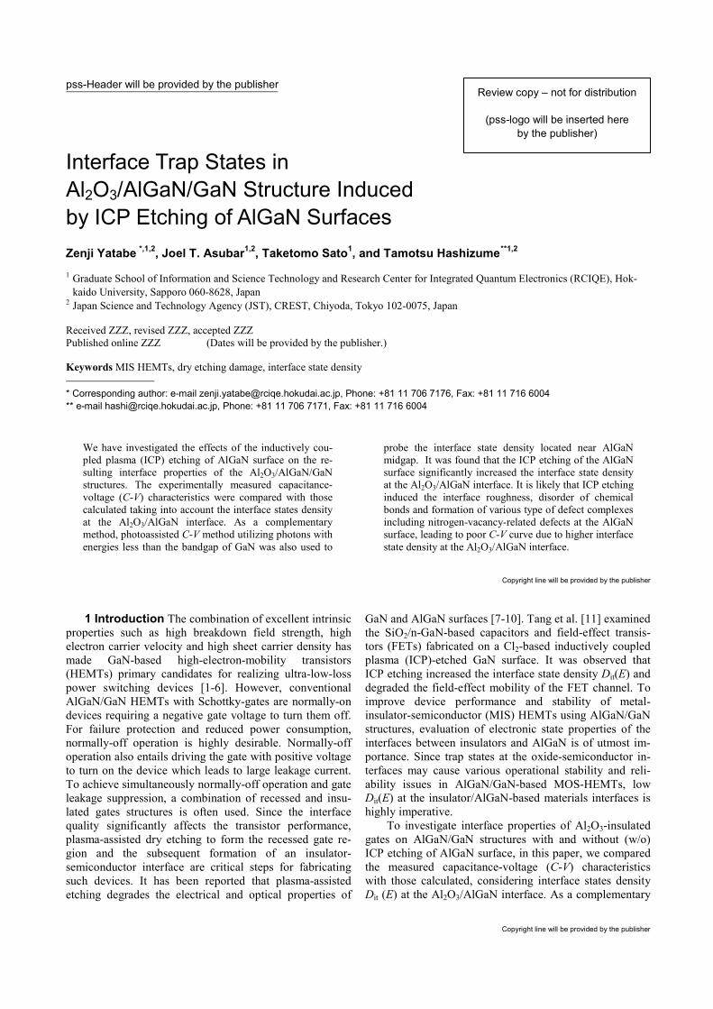
Figure 1 Schematic illustration of the Al2O3/Al0.2Ga0.8N/GaN structure used in this study.
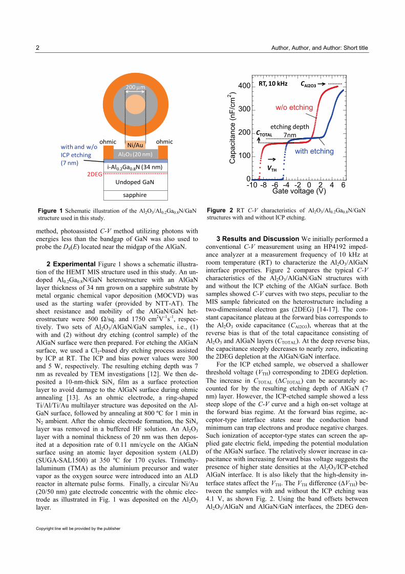
Figure 2 RT C-V characteristics of Al2O3/Al0.2Ga0.8N/GaN structures with and without ICP etching.
method, photoassisted C-V method utilizing photons with energies less than the bandgap of GaN was also used to probe the Dit(E) located near the midgap of the AlGaN.
2 Experimental Figure 1 shows a schematic illustra-tion of the HEMT MIS structure used in this study. An un-doped Al0.2Ga0.8N/GaN heterostructure with an AlGaN layer thickness of 34 nm grown on a sapphire substrate by metal organic chemical vapor deposition (MOCVD) was used as the starting wafer (provided by NTT-AT). The sheet resistance and mobility of the AlGaN/GaN het-erostructure were 500 Ω/sq. and 1750 cm2V-1s-1, respec-tively. Two sets of Al2O3/AlGaN/GaN samples, i.e., (1) with and (2) without dry etching (control sample) of the AlGaN surface were then prepared. For etching the AlGaN surface, we used a Cl2-based dry etching process assisted by ICP at RT. The ICP and bias power values were 300 and 5 W, respectively. The resulting etching depth was 7 nm as revealed by TEM investigations [12]. We then de-posited a 10-nm-thick SiNx film as a surface protection layer to avoid damage to the AlGaN surface during ohmic annealing [13]. As an ohmic electrode, a ring-shaped Ti/Al/Ti/Au multilayer structure was deposited on the Al-GaN surface, followed by annealing at 800 ºC for 1 min in N2 ambient. After the ohmic electrode formation, the SiNx layer was removed in a buffered HF solution. An Al2O3 layer with a nominal thickness of 20 nm was then depos-ited at a deposition rate of 0.11 nm/cycle on the AlGaN surface using an atomic layer deposition system (ALD) (SUGA-SAL1500) at 350 ºC for 170 cycles. Trimethy-laluminum (TMA) as the aluminium precursor and water vapor as the oxygen source were introduced into an ALD reactor in alternate pulse forms. Finally, a circular Ni/Au (20/50 nm) gate electrode concentric with the ohmic elec-trode as illustrated in Fig. 1 was deposited on the Al2O3 layer.
3 Results and Discussion We initially performed a
conventional C-V measurement using an HP4192 imped-ance analyzer at a measurement frequency of 10 kHz at room temperature (RT) to characterize the Al2O3/AlGaN interface properties. Figure 2 compares the typical C-V characteristics of the Al2O3/AlGaN/GaN structures with and without the ICP etching of the AlGaN surface. Both samples showed C-V curves with two steps, peculiar to the MIS sample fabricated on the heterostructure including a two-dimensional electron gas (2DEG) [14-17]. The con-stant capacitance plateau at the forward bias corresponds to the Al2O3 oxide capacitance (CAl2O3), whereas that at the reverse bias is that of the total capacitance consisting of Al2O3 and AlGaN layers (CTOTAL). At the deep reverse bias, the capacitance steeply decreases to nearly zero, indicating the 2DEG depletion at the AlGaN/GaN interface.
For the ICP etched sample, we observed a shallower threshold voltage (VTH) corresponding to 2DEG depletion. The increase in CTOTAL (∆CTOTAL) can be accurately ac-counted for by the resulting etching depth of AlGaN (7 nm) layer. However, the ICP-etched sample showed a less steep slope of the C-V curve and a high on-set voltage at the forward bias regime. At the forward bias regime, ac-ceptor-type interface states near the conduction band minimum can trap electrons and produce negative charges. Such ionization of acceptor-type states can screen the ap-plied gate electric field, impeding the potential modulation of the AlGaN surface. The relatively slower increase in ca-pacitance with increasing forward bias voltage suggests the presence of higher state densities at the Al2O3/ICP-etched AlGaN interface. It is also likely that the high-density in-terface states affect the VTH. The VTH difference (∆VTH) be-tween the samples with and without the ICP etching was 4.1 V, as shown Fig. 2. Using the band offsets between Al2O3/AlGaN and AlGaN/GaN interfaces, the 2DEG den-
Al2O3 (20 nm)
sapphire
Undoped GaN
i-Al0.2Ga0.8N (34 nm)2DEG
ohmicohmic
200 µm
Ni/Auwith and w/o ICP etching(7 nm)
-10 -8 -6 -4 -2 0 2 4 60
100
200
300
400
Cap
acita
nce
(nF/
cm2 )
Gate voltage (V)
w/o etching
with etching
etching depth7nm
VTH
RT, 10 kHz
CTOTAL
CAl2O3
pss-Header will be provided by the publisher 3
Copyright line will be provided by the publisher
1 2 3 4 5 6 7 8 9 10 11 12 13 14 15 16 17 18 19 20 21 22 23 24 25 26 27 28 29 30 31 32 33 34 35 36 37 38 39 40 41 42 43 44 45 46 47 48 49 50 51 52 53 54 55 56 57
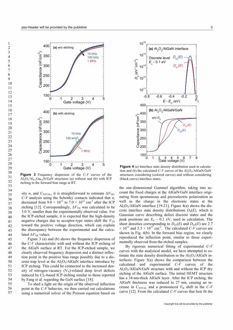
Figure 3 Frequency dispersion of the C-V curves of the Al2O3/Al0.2Ga0.8N/GaN structures (a) without and (b) with ICP etching in the forward bias range at RT.
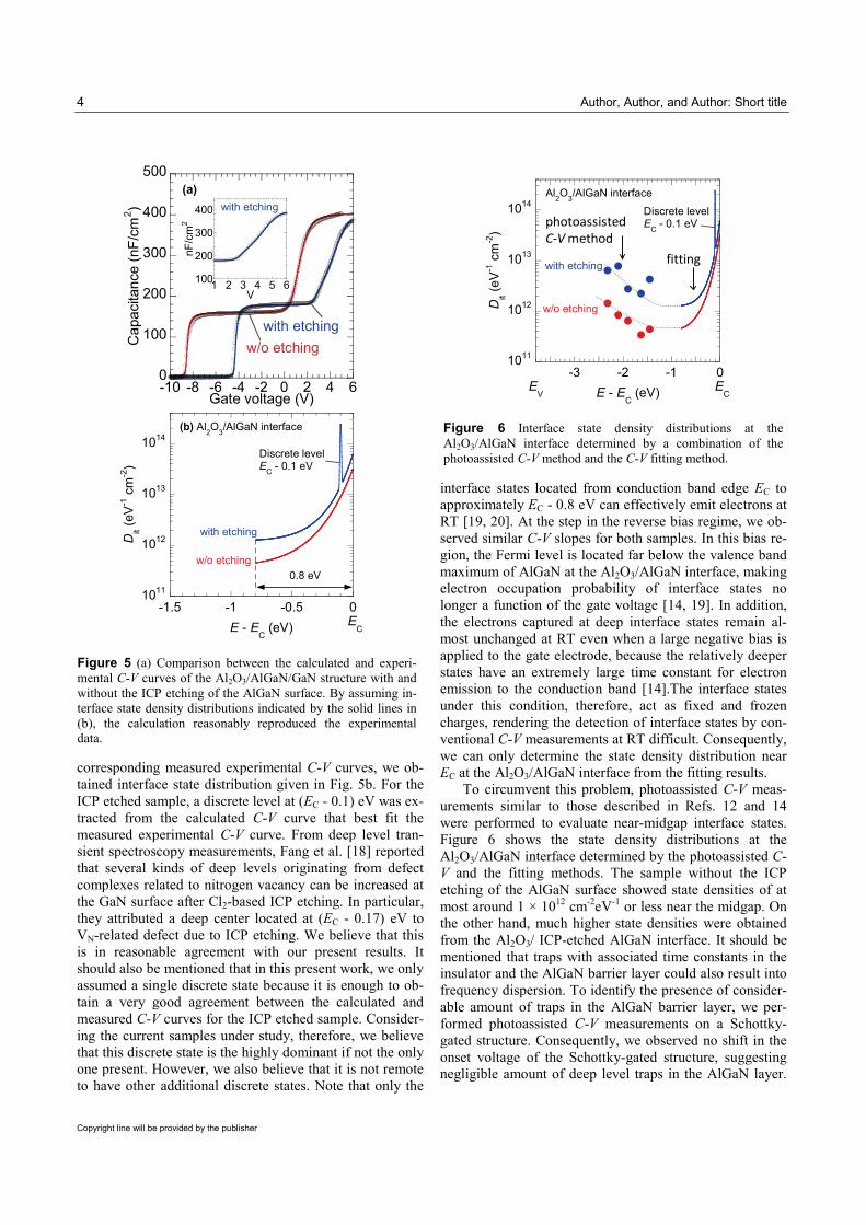
Figure 4 (a) Interface state density distribution used in calcula-tion and (b) the calculated C-V curves of the Al2O3/AlGaN/GaN structures considering (colored curves) and without considering (black curve) interface states.
sity ns and CTOTAL, it is straightforward to estimate ∆VTH. C-V analysis using the Schottky contacts indicated that ns decreased from 9.0 × 10¹² to 7.0 × 1012 cm-2 after the ICP etching [12]. Correspondingly, ∆VTH was calculated to be 3.0 V, smaller than the experimentally observed value. For the ICP-etched sample, it is expected that the high-density negative charges due to acceptor-type states shift the VTH toward the positive voltage direction, which can explain the discrepancy between the experimental and the calcu-lated ∆VTH values.
Figure 3 (a) and (b) shows the frequency dispersion of the C-V characteristic with and without the ICP etching of the AlGaN surface at RT. For the ICP-etched sample, we clearly observed frequency dispersion and a distinct inflec-tion point in the positive bias range possibly due to a dis-crete trap level at the Al2O3/AlGaN interface introduce by ICP etching. This could be connected to the increased den-sity of nitrogen-vacancy (VN)-related deep level defects induced by Cl2-based ICP etching similar to those reported by Fang et al. regarding the GaN surface [18].
To shed a light on the origin of the observed inflection point in the C-V behavior, we then carried out calculations using a numerical solver of the Poisson equation based on
the one-dimensional Gummel algorithm, taking into ac-count the fixed charges at the AlGaN/GaN interface origi-nating from spontaneous and piezoelectric polarization as well as the charge in the electronic states at the Al2O3/AlGaN interface [19-21]. Figure 4(a) shows the dis-crete interface state density distributions Dit(E), which is Gaussian curve describing defect discrete states and the peak positions are EC - 0.1 eV, used in calculation. The sheet densities corresponding to Dit1(E) and Dit2(E) are 2.7 × 10¹² and 5.3 × 1012 cm-2. The calculated C-V curves are shown in Fig. 4(b). In the forward bias region, we clearly reproduced the inflection point, similar to those experi-mentally observed from the etched samples.
By rigorous numerical fitting of experimental C-V curves with the analytical model, we have attempted to es-timate the state density distribution in the Al2O3/AlGaN in-terfaces. Figure 5(a) shows the comparison between the calculated and experimental C-V curves of the Al2O3/AlGaN/GaN structure with and without the ICP dry etching of the AlGaN surface. The initial HEMT structure has a 34-nm-thick AlGaN layer. After the ICP etching, the AlGaN thickness was reduced to 27 nm, causing an in-crease in CTOTAL and a pronounced Vth shift in the C-V curve [12]. From the calculated C-V curves that best fit the
0 1 2 3 4 5150
200
250
300
350
400
Cap
acita
nce
(nF/
cm2 )
Gate voltage (V)
(b) with etching
1 MHz
10 kHz100 kHz
0 1 2 3 4 5150
200
250
300
350
400C
apac
itanc
e (n
F/cm
2 )
Gate voltage (V)
(a) w/o etching
10 kHz100 kHz1 MHz
0 1 2 3 4 5 6 7 8150
200
250
300
350
400
450
Cap
acita
nce
(nF/
cm2 )
Gate voltage (V)
Dit1(E)
w/o Dit
Dit2(E)
(b) Al2O
3/AlGaN/GaN
-0.8 -0.6 -0.4 -0.2 0
1011
1012
1013
1014
1015
Dit (e
V-1
cm-2
)
E - EC (eV) E
C
Dit1
(E)
(a) Al2O
3/AlGaN interface
Discrete levelE
c - 0.1 eV
Dit2
(E)
4 Author, Author, and Author: Short title
Copyright line will be provided by the publisher
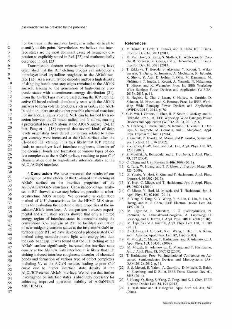
Figure 5 (a) Comparison between the calculated and experi-mental C-V curves of the Al2O3/AlGaN/GaN structure with and without the ICP etching of the AlGaN surface. By assuming in-terface state density distributions indicated by the solid lines in (b), the calculation reasonably reproduced the experimental data.
Figure 6 Interface state density distributions at the Al2O3/AlGaN interface determined by a combination of the photoassisted C-V method and the C-V fitting method.
corresponding measured experimental C-V curves, we ob-tained interface state distribution given in Fig. 5b. For the ICP etched sample, a discrete level at (EC - 0.1) eV was ex-tracted from the calculated C-V curve that best fit the measured experimental C-V curve. From deep level tran-sient spectroscopy measurements, Fang et al. [18] reported that several kinds of deep levels originating from defect complexes related to nitrogen vacancy can be increased at the GaN surface after Cl2-based ICP etching. In particular, they attributed a deep center located at (EC - 0.17) eV to VN-related defect due to ICP etching. We believe that this is in reasonable agreement with our present results. It should also be mentioned that in this present work, we only assumed a single discrete state because it is enough to ob-tain a very good agreement between the calculated and measured C-V curves for the ICP etched sample. Consider-ing the current samples under study, therefore, we believe that this discrete state is the highly dominant if not the only one present. However, we also believe that it is not remote to have other additional discrete states. Note that only the
interface states located from conduction band edge EC to approximately EC - 0.8 eV can effectively emit electrons at RT [19, 20]. At the step in the reverse bias regime, we ob-served similar C-V slopes for both samples. In this bias re-gion, the Fermi level is located far below the valence band maximum of AlGaN at the Al2O3/AlGaN interface, making electron occupation probability of interface states no longer a function of the gate voltage [14, 19]. In addition, the electrons captured at deep interface states remain al-most unchanged at RT even when a large negative bias is applied to the gate electrode, because the relatively deeper states have an extremely large time constant for electron emission to the conduction band [14].The interface states under this condition, therefore, act as fixed and frozen charges, rendering the detection of interface states by con-ventional C-V measurements at RT difficult. Consequently, we can only determine the state density distribution near EC at the Al2O3/AlGaN interface from the fitting results.
To circumvent this problem, photoassisted C-V meas-urements similar to those described in Refs. 12 and 14 were performed to evaluate near-midgap interface states. Figure 6 shows the state density distributions at the Al2O3/AlGaN interface determined by the photoassisted C-V and the fitting methods. The sample without the ICP etching of the AlGaN surface showed state densities of at most around 1 × 1012 cm-2eV-1 or less near the midgap. On the other hand, much higher state densities were obtained from the Al2O3/ ICP-etched AlGaN interface. It should be mentioned that traps with associated time constants in the insulator and the AlGaN barrier layer could also result into frequency dispersion. To identify the presence of consider-able amount of traps in the AlGaN barrier layer, we per-formed photoassisted C-V measurements on a Schottky-gated structure. Consequently, we observed no shift in the onset voltage of the Schottky-gated structure, suggesting negligible amount of deep level traps in the AlGaN layer.
0 1 2 3 4 5 6 7 8150
200
250
300
350
400
450
Cap
acita
nce
(nF/
cm2 )
Gate voltage (V)
Dit1(E)
w/o Dit
Dit2(E)
(b) Al2O
3/AlGaN/GaN
-0.8 -0.6 -0.4 -0.2 0
1011
1012
1013
1014
1015
Dit (e
V-1
cm-2
)
E - EC (eV) E
C
Dit1
(E)
(a) Al2O
3/AlGaN interface
Discrete levelE
c - 0.1 eV
Dit2
(E)
1 2 3 4 5 6100
200
300
400
nF/c
m2
V
with etching
1011
1012
1013
1014
-1.5 -1 -0.5 0
Dit (e
V-1
cm
-2)
E - EC (eV)
Discrete levelEC - 0.1 eV
0.8 eV
EC
with etching
w/o etching
(b) Al2O3/AlGaN interface
-10 -8 -6 -4 -2 0 2 4 60
100
200
300
400
500
Cap
acita
nce
(nF/
cm2 )
Gate voltage (V)
w/o etchingwith etching
(a)
1011
1012
1013
1014
-3 -2 -1 0
Dit (e
V-1
cm
-2)
E - EC (eV) E
CE
V
with etching
w/o etching
Discrete levelEC - 0.1 eV
Al2O3/AlGaN interface
photoassistedC-V method
fitting
pss-Header will be provided by the publisher 5
Copyright line will be provided by the publisher
1 2 3 4 5 6 7 8 9 10 11 12 13 14 15 16 17 18 19 20 21 22 23 24 25 26 27 28 29 30 31 32 33 34 35 36 37 38 39 40 41 42 43 44 45 46 47 48 49 50 51 52 53 54 55 56 57
For the traps in the insulator layer, it is rather difficult to quantify at this point. Nevertheless, we believe that inter-face states are the most dominant cause of frequency dis-persion as explicitly stated in Ref. [22] and mathematically described in Ref. [23].
Transmission electron microscope observations have established that the ICP etching process can introduce a monolayer-level crystalline roughness to the AlGaN sur-face [12]. As a result, lattice disorder and/or a high density of dangling bonds near step edges remained at the AlGaN surface, leading to the generation of high-density elec-tronic states with a continuous energy distribution [21]. From the Cl2/BCl gas mixture used during the ICP etching, active Cl-based radicals dominantly react with the AlGaN surfaces to form volatile products, such as GaCl3 and AlCl3. In addition, there are also other possible chemical reactions. For instance, a highly volatile NCl3 can be formed by a re-action between the Cl-based radical and N atoms, causing a preferential loss of N atoms at the AlGaN surface [24]. In fact, Fang et al. [18] reported that several kinds of deep levels originating from defect complexes related to nitro-gen vacancy were increased at the GaN surface after the Cl2-based ICP etching. It is thus likely that ICP etching leads to monolayer-level interface roughness, disorder of the chemical bonds and formation of various types of de-fect complexes at the AlGaN surface, resulting to poor C-V characteristics due to high-density interface states at the Al2O3/AlGaN interface.
4 Conclusion We have presented the results of our
investigation of the effects of the Cl2-based ICP etching of AlGaN surface on the interface properties of the Al2O3/AlGaN/GaN structures. Capacitance-voltage analy-ses at RT showed a two-step behavior, peculiar to a het-erostructure MOS sample. We presented a calculation method of C-V characteristics for the HEMT MIS struc-tures for evaluating the electronic state properties at the in-sulator/AlGaN interfaces. A comparison between experi-mental and simulation results showed that only a limited energy region of interface states is detectable using the conventional C-V analysis at RT. To facilitate evaluation of near-midgap electronic states at the insulator/AlGaN in-terfaces under RT, we have developed a photoassisted C-V method using monochromatic light with energy less than the GaN bandgap. It was found that the ICP etching of the AlGaN surface significantly increased the interface state density at the Al2O3/AlGaN interface. It is likely that ICP etching induced interface roughness, disorder of chemical bonds and formation of various type of defect complexes including VN at the AlGaN surface, leading to poor C-V curve due to higher interface state density at the Al2O3/ICP-etched AlGaN interface. We believe that further investigation on interface states is absolutely necessary for achieving improved operation stability of AlGaN/GaN MIS HEMTs.
References [1] M. Ishida, T. Ueda, T. Tanaka, and D. Ueda, IEEE Trans.
Electron Dev. 60, 3053 (2013). [2] M. Van Hove, X. Kang, S. Stoffels, D. Wellekens, N. Ron-
chi, R. Venegas, K. Geens, and S. Decoutere, IEEE Trans. Electron Dev. 60, 3071 (2013).
[3] T. Kikkawa, T. Hosoda, S. Akiyama, Y. Kotani, T. Waka-bayashi, T. Ogino, K. Imanishi, A. Mochizuki, K. Itabashi, K. Shono, Y. Asai, K. Joshin, T. Ohki, M. Kanamura, M. Nishimori, T. Imada, J. Kotani, A. Yamada, N. Nakamura, T. Hirose, and K. Watanabe, Proc. 1st IEEE Workshop Wide Bandgap Power Devices and Application (WiPDA-2013), 2013, p. 11.
[4] B. Hughes, R. Chu, J. Lazar, S. Hulsey, A. Carrido, D. Zehnder, M. Musni, and K. Boutros, Proc. 1st IEEE Work-shop Wide Bandgap Power Devices and Application (WiPDA-2013), 2013, p. 76.
[5] Y.-F. Wu, J. Gritters, L. Shen, R. P. Smith, J. McKay, and R. Birkhahn, Proc. 1st IEEE Workshop Wide Bandgap Power Devices and Application (WiPDA-2013), 2013, p. 6.
[6] N. Herbecq, I. Roch-Jeune, N. Rolland, D. Visalli, J. Der-luyn, S. Degroote, M. Germain, and F. Medjdoub, Appl. Phys. Express 7, 034103 (2014).
[7] J. Kuzmík, P. Javorka, M. Marso, and P. Kordos, Semicond. Sci. Technol. 17, L76 (2002).
[8] K.-J. Choi, H.-W. Jang, and J.-L. Lee, Appl. Phys. Lett. 82, 1233 (2003).
[9] Z. Mouffak, A. Bensaoula, and L. Trombetta, J. Appl. Phys. 95, 727 (2004).
[10] C. Cheng and J. Si: Physica B 406, 3098 (2011). [11] K. Tang, W. Huang, and T. P. Chow, J. Electron. Mater. 38,
523 (2009). [12] Z. Yatabe, Y. Hori, S. Kim, and T. Hashizume, Appl. Phys.
Express 6, 016502 (2013). [13] Y. Hori, C. Mizue, and T. Hashizume, Jpn. J. Appl. Phys.
49, 080201 (2010). [14] C. Mizue, Y. Hori, M. Miczek, and T. Hashizume, Jpn. J.
Appl. Phys. 50, 021001 (2011). [15] S. Yang, Z. Tang, K.-Y. Wong, Y.-S. Lin, C. Liu, Y. Lu, S.
Huang, and K. J. Chen, IEEE Electron Device Lett. 34, 1497 (2013).
[16] M. Fagerlind, F. Allerstam, E. Ö. Sveinbjörnsson, N. Rorsman, A. Kakanakova-Georgieva, A. Lundskog, U. Forsberg, and E. Janzén, J. Appl. Phys. 108, 014508 (2010).
[17] M. Ťapajna and J. Kuzmík, Appl. Phys. Lett. 100, 113509 (2012).
[18] Z.-Q. Fang, D. C. Look, X.-L. Wang, J. Han, F. A. Khan, and I. Adesida, Appl. Phys. Lett. 82, 1562 (2003).
[19] M. Miczek, C. Mizue, T. Hashizume, and B. Adamowicz, J. Appl. Phys. 103, 104510 (2008).
[20] M. Miczek, B. Adamowicz, C. Mizue, and T. Hashizume, Jpn. J. Appl. Phys. 48, 04C092 (2009).
[21] T. Hashizume, Proc. 9th International Conference on Ad-vanced Semiconductor Devices and Microsystems (AS-DAM 2012), 2012, p. 31.
[22] S. S. Mehari, E. Yalon, A. Gavrilov, D. Mistele, G. Bahir, M. Eizenberg, and D. Ritter, IEEE Trans. Electron Dev. 61, 3558 (2014).
[23] S. Huang, Q. Jiang, S. Yang, Z. Tang, and K. J. Chen, IEEE Electron Device Lett. 34, 193 (2013).
[24] T. Hashizume and H. Hasegawa, Appl. Surf. Sci. 234, 387 (2004).