Embed Size (px)
Citation preview
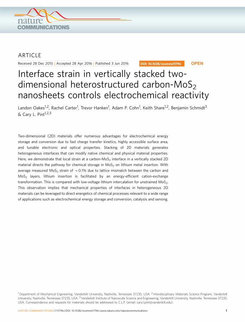
ARTICLE
Received 28 Dec 2015 | Accepted 28 Apr 2016 | Published 3 Jun 2016
Interface strain in vertically stacked two-dimensional heterostructured carbon-MoS2
nanosheets controls electrochemical reactivityLandon Oakes1,2, Rachel Carter1, Trevor Hanken1, Adam P. Cohn1, Keith Share1,2, Benjamin Schmidt3
& Cary L. Pint1,2,3
Two-dimensional (2D) materials offer numerous advantages for electrochemical energy
storage and conversion due to fast charge transfer kinetics, highly accessible surface area,
and tunable electronic and optical properties. Stacking of 2D materials generates
heterogeneous interfaces that can modify native chemical and physical material properties.
Here, we demonstrate that local strain at a carbon-MoS2 interface in a vertically stacked 2D
material directs the pathway for chemical storage in MoS2 on lithium metal insertion. With
average measured MoS2 strain of B0.1% due to lattice mismatch between the carbon and
MoS2 layers, lithium insertion is facilitated by an energy-efficient cation-exchange
transformation. This is compared with low-voltage lithium intercalation for unstrained MoS2.
This observation implies that mechanical properties of interfaces in heterogeneous 2D
materials can be leveraged to direct energetics of chemical processes relevant to a wide range
of applications such as electrochemical energy storage and conversion, catalysis and sensing.
DOI: 10.1038/ncomms11796 OPEN
1 Department of Mechanical Engineering, Vanderbilt University, Nashville, Tennessee 37235, USA. 2 Interdisciplinary Materials Science Program, VanderbiltUniversity, Nashville, Tennessee 37235, USA. 3 Vanderbilt Institute of Nanoscale Science and Engineering, Vanderbilt University, Nashville, Tennessee 37235,USA. Correspondence and requests for materials should be addressed to C.L.P. (email: [email protected]).
NATURE COMMUNICATIONS | 7:11796 | DOI: 10.1038/ncomms11796 | www.nature.com/naturecommunications 1
2Dgraphene and transition metal dichalcogenide
(TMDC) materials have captivated researchers inthe past decade owing to a set of unique physical
and chemical properties that deviate from their bulk analoguesand the exploitation of these properties in broad applications1.Specifically for electronics, vertical integration of 2D materialsenables logic component design with high on-off ratio andpromise for three-dimensional (3D) electronics that progressbeyond silicon2–8. In semiconductor electronics, engineering 2DTMDC materials using strain applied at an interface has beenshown to strongly modulate the bandgap and band structure,which results in modified electrical and optical propertiesfor strained materials9–14. For monolayer MoS2, the bandgap isobserved to shift by up to 15 meV under tensile strain of up to4.8% (ref. 15), and for multilayered WSe2 the bandgap transitionsfrom indirect to direct under strain of up to 2% (ref. 16).Theoretical efforts have further emphasized strain-enabledbroadband absorption and photodetection in MoS2, eventhough this has not yet been experimentally realized17. Theintersection of strain-engineered properties of 2D materials andheterostructured vertically integrated interfaces of 2D materialspresents an engaging research area for next-generationelectronics. Nonetheless, such materials and research directionsremain elusive for many other applications of 2D materials.
On this front, 2D materials and specifically 2D TMDCs havedemonstrated excellent performance in a range of electrochemicalapplications including lithium- and sodium-ion batteries18–20,photocatalytic conversion21–23 and biosensing applications24–26.Unlike electronic devices, these applications require bulk-likequantities of 2D materials—a challenge aided by recentdevelopments in the liquid exfoliation and assembly of layeredTMDCs27–29. However, addressing how properties inheterostructured or complex 2D materials can impact chemicalprocesses responsible for electrochemical applications is hamperedby uniform material fabrication routes that can be used on scalesrequired for electrochemical measurements. As a result, the impactof strained interfaces in 2D materials on chemical andelectrochemical processes remains virtually unstudied. Onlyrecently has an observation emerged that compressive strain onPt catalysts can improve the oxygen reduction reaction capabilityof Pt relevant to fuel cells30. In this manner, 2D materials providean ideal test bed for the understanding of how interfaces and straincan impact electrochemical processes, motivated by pioneeringefforts in the field of semiconductor electronics.
This is the focus of this report, which documents that interfacestrain measured over statistical quantities of stacked 2Dcarbon-MoS2 heterostructured nanosheets can be directly corre-lated with distinct differences in chemical processes occurring in2D materials. In particular, combining optical and electro-chemical techniques we demonstrate that strain engineering ofinterfaces can enable control of the energetic pathway for thechemical conversion of MoS2 into electrochemically active Moand Li2Sn species during reaction with lithium. This highlights theimportant role that mechanical strain can have in engineeringenergy storage processes in materials.
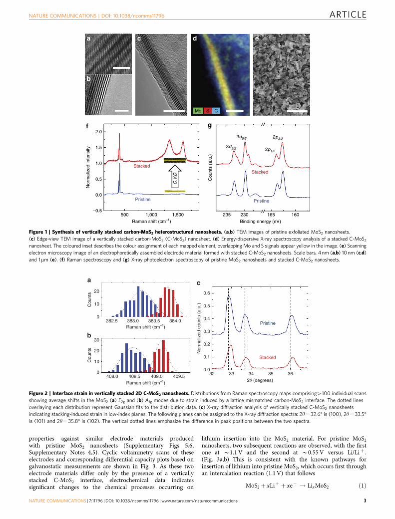
ResultsFabrication of interface-strained materials. MoS2 nanosheetswere produced through liquid exfoliation of bulk MoS2 powdersin n-methyl-2-pyrrolidone (NMP) solvents and subsequent cen-trifugation. Transmission electron microscopy (TEM) of arepresentative exfoliated MoS2 nanosheet is shown in Fig. 1a,b.Interlayer spacing of B0.61 nm is observed for MoS2
nanosheets, with thicknesses ranging from 2–15 atomic layers(Supplementary Fig. 1, Supplementary Note 1). Ultrathin carbon
layers are grown directly on the MoS2 surface through MoS2
catalysed decomposition of C2H2 precursors using atemperature ramp chemical vapour deposition process(Supplementary Fig. 2) that is capable of gram-scale batchprocessing. This generates vertically stacked architectures whereultrathin carbon layers are formed on both sides of the MoS2
nanosheets, with a representative TEM image of this architectureshown in Fig. 1c, and corresponding elemental analysis map inFig. 1d. To produce an appreciable mass of material forelectrochemical tests, electrophoretic deposition was used toassemble the vertically stacked carbon-interfaced MoS2 (C-MoS2)nanosheets into conformal films on metal substrates from NMPdispersions following chemical vapour deposition (Fig. 1e;Supplementary Fig. 3, Supplementary Note 2). All aspects ofsynthesis and processing of C-MoS2 materials are chosen to becompatible with scalable processing, and ongoing research effortsto improve the simplicity and scalability of liquid exfoliation canfurther improve this31. Raman spectroscopy analysis (Fig. 1f) ofvertically stacked C-MoS2 nanosheets indicates that vertical stacksmaintain an identical signature of crystalline MoS2 following thecarbon synthesis based on E2g and A1g modes (300–500 cm� 1).The carbon layers exhibit a significant amount of sp3 hybridizedcarbon atoms (B1,320 cm� 1, or D-band) relative to sp2 carbonspecies (B1,580 cm� 1, or G-band). Whereas this indicatesthe presence of carbon, X-ray photoelectron spectroscopy (XPS)indicates the emergence of both a peak in the sulfur 2p3/2 and2p5/2 spectra at low-binding energies, as well as shoulders inboth Mo 3d5/2 and 3d3/2 peaks that represent a modulation tothe local bonding environment in the crystal (Fig. 1g). Notably,the existence of the low-energy shoulder in the sulfur 2p andMo 3d peaks is consistent with the formation of the metallic1T-phase of MoS2 produced from the strain-induced distortionof sulfur atoms observed previously (Supplementary Fig. 4,Supplementary Note 3)32. This analysis collectively supports theformation of a distinct carbon-MoS2 stacked interface, wheremismatch of the in-plane lattice spacing between MoS2 andcarbon will induce significant interface strain that propagates intothe MoS2 nanosheet from the C-MoS2 interface.
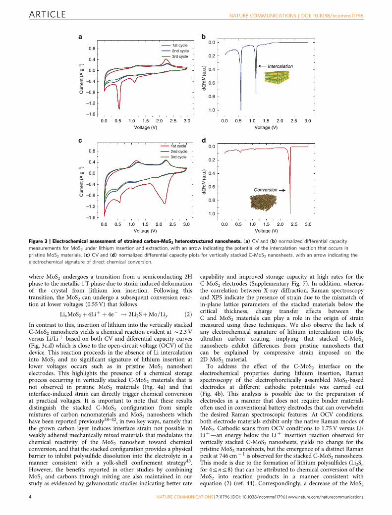
To assess strain in the vertically stacked 2D material, statisticalRaman spectroscopy mapping comprising over 200 individualscans in separate areas was performed on the E2g and A1g modesof MoS2, which are highly sensitive to tensile or compressivestrain33–35. (Fig. 2a,b) On the basis of the peak-to-peak analysis ofRaman mode distributions, blue-shifts of B0.66 cm� 1 andB0.59 cm� 1 were observed for the E2g and A1g modes,respectively. Asymmetry in these modes is expected andattributed to stronger electronic coupling to the A1g mode36.This yields an B0.1–0.2% compressive strain based on relativeA1g mode shifts in accordance with previous studies9,34,supporting the presence of interface-induced compressive strainon the MoS2 material. This is further confirmed using X-raydiffraction which demonstrates a similar B0.1% compressivestrain due to vertical stacking based on analysis of the (100) and(110) low-index planes of MoS2 (Fig. 2c). We anticipate thismeasured strain to be present at both the interface and on theinterior of the nanosheets as they possess a thickness well belowthe critical layer thickness at which strain relaxation occurs37.
Controlling electrochemical processes using strain. To assesshow the vertically stacked architecture and interfacestrain influences electrochemical processes, we combinedelectrophoretically assembled vertically stacked 2D C-MoS2
nanosheets with Li metal electrodes, and a 1.0 M lithiumhexafluorophosphate solution in ethylene carbonate and diethylcarbonate electrolyte, and compared the electrochemical
ARTICLE NATURE COMMUNICATIONS | DOI: 10.1038/ncomms11796
2 NATURE COMMUNICATIONS | 7:11796 | DOI: 10.1038/ncomms11796 | www.nature.com/naturecommunications
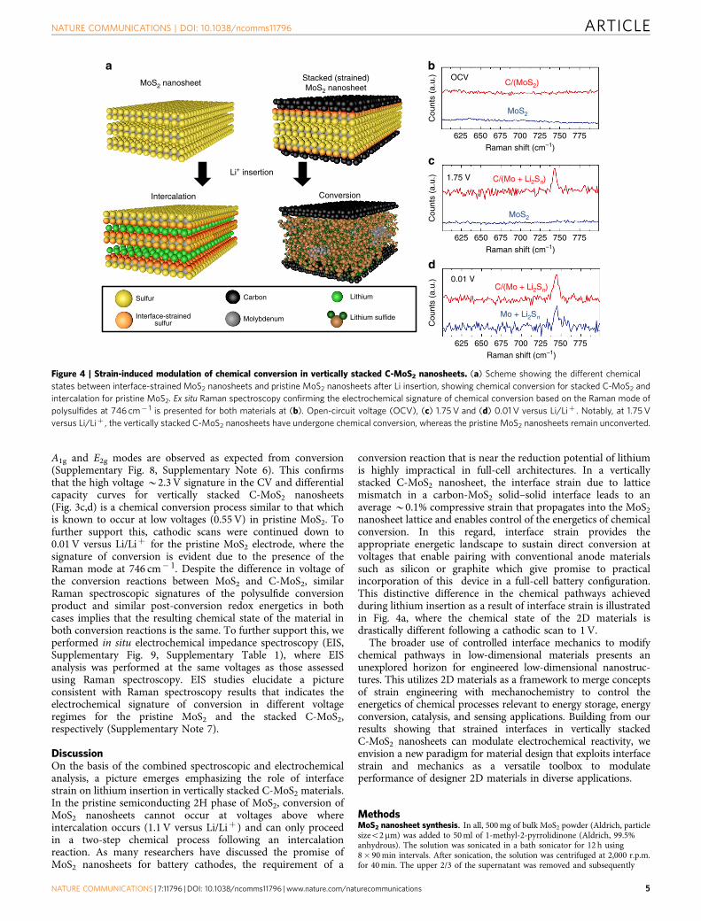
properties against similar electrode materials producedwith pristine MoS2 nanosheets (Supplementary Figs 5,6,Supplementary Notes 4,5). Cyclic voltammetry scans of theseelectrodes and corresponding differential capacity plots based ongalvanostatic measurements are shown in Fig. 3. As these twoelectrode materials differ only by the presence of a verticallystacked C-MoS2 interface, electrochemical data indicatessignificant changes to the chemical processes occurring on
lithium insertion into the MoS2 material. For pristine MoS2
nanosheets, two subsequent reactions are observed, with the firstone at B1.1 V and the second at B0.55 V versus Li/Liþ .(Fig. 3a,b) This is consistent with the known pathways forinsertion of lithium into pristine MoS2, which occurs first throughan intercalation reaction (1.1 V) that follows
MoS2þ xLiþ þ xe� ! LixMoS2 ð1Þ
20
a
b
c0.6
0.5
0.4
0.3
0.2
0.1
0.032 33 34
2� (degrees)35 36
20
30
Cou
nts
Cou
nts
Nor
mal
ized
cou
nts
(a.u
.)10
10
0
0
382.5 383.0Raman shift (cm–1)
Pristine
Stacked
383.5 384.0
408.0 408.5Raman shift (cm–1)
409.0 409.5
Figure 2 | Interface strain in vertically stacked 2D C-MoS2 nanosheets. Distributions from Raman spectroscopy maps comprising4100 individual scans
showing average shifts in the MoS2 (a) E2g and (b) A1g modes due to strain induced by a lattice mismatched carbon-MoS2 interface. The dotted lines
overlaying each distribution represent Gaussian fits to the distribution data. (c) X-ray diffraction analysis of vertically stacked C-MoS2 nanosheets
indicating stacking-induced strain in low-index planes. The following planes can be assigned to the X-ray diffraction spectra: 2y¼ 32.6� is (100), 2y¼ 33.5�is (101) and 2y¼ 35.8� is (102). The vertical dotted lines emphasize the difference in peak positions between the two spectra.
2.0f g
a c d e
b
1.5
1.0
Nor
mal
ized
inte
nsity
Cou
nts
(a.u
.)
0.5
0.0
–0.5500
PristinePristine
StackedStacked
C.V.D
1,000Raman shift (cm–1)
1,500 235
Mo S C
230
3d3/2
3d5/2
2p1/2
2p3/2
165
Binding energy (eV)
160
Figure 1 | Synthesis of vertically stacked carbon-MoS2 heterostructured nanosheets. (a,b) TEM images of pristine exfoliated MoS2 nanosheets.
(c) Edge-view TEM image of a vertically stacked carbon-MoS2 (C-MoS2) nanosheet. (d) Energy-dispersive X-ray spectroscopy analysis of a stacked C-MoS2
nanosheet. The coloured inset describes the colour assignment of each mapped element, overlapping Mo and S signals appear yellow in the image. (e) Scanning
electron microscopy image of an electrophoretically assembled electrode material formed with stacked C-MoS2 nanosheets. Scale bars, 4 nm (a,b) 10 nm (c,d)
and 1mm (e). (f) Raman spectroscopy and (g) X-ray photoelectron spectroscopy of pristine MoS2 nanosheets and stacked C-MoS2 nanosheets.
NATURE COMMUNICATIONS | DOI: 10.1038/ncomms11796 ARTICLE
NATURE COMMUNICATIONS | 7:11796 | DOI: 10.1038/ncomms11796 | www.nature.com/naturecommunications 3
where MoS2 undergoes a transition from a semiconducting 2Hphase to the metallic 1 T phase due to strain-induced deformationof the crystal from lithium ion insertion. Following thistransition, the MoS2 can undergo a subsequent conversion reac-tion at lower voltages (0.55 V) that follows
LixMoS2þ 4Liþ þ 4e� ! 2Li2SþMo=Liy ð2ÞIn contrast to this, insertion of lithium into the vertically stackedC-MoS2 nanosheets yields a chemical reaction evident at B2.3 Vversus Li/Liþ based on both CV and diferential capacity curves(Fig. 3c,d) which is close to the open-circuit voltage (OCV) of thedevice. This reaction proceeds in the absence of Li intercalationinto MoS2 and no significant signature of lithium insertion atlower voltages occurs such as in pristine MoS2 nanosheetelectrodes. This highlights the presence of a chemical storageprocess occurring in vertically stacked C-MoS2 materials that isnot observed in pristine MoS2 materials (Fig. 4a) and thatinterface-induced strain can directly trigger chemical conversionat practical voltages. It is important to note that these resultsdistinguish the stacked C-MoS2 configuration from simplemixtures of carbon nanomaterials and MoS2 nanosheets whichhave been reported previously38–42, in two key ways, namely thatthe grown carbon layer induces interface strain not possible inweakly adhered mechanically mixed materials that modulates thechemical reactivity of the MoS2 nanosheet toward chemicalconversion, and that the stacked configuration provides a physicalbarrier to inhibit polysulfide dissolution into the electrolyte in amanner consistent with a yolk-shell confinement strategy43.However, the benefits reported in other studies by combiningMoS2 and carbons through mixing are also maintained in ourstudy as evidenced by galvanostatic studies indicating better rate
capability and improved storage capacity at high rates for theC-MoS2 electrodes (Supplementary Fig. 7). In addition, whereasthe correlation between X-ray diffraction, Raman spectroscopyand XPS indicate the presence of strain due to the mismatch ofin-plane lattice parameters of the stacked materials below thecritical thickness, charge transfer effects between theC and MoS2 materials can play a role in the origin of strainmeasured using these techniques. We also observe the lack ofany electrochemical signature of lithium intercalation into theultrathin carbon coating, implying that stacked C-MoS2
nanosheets exhibit differences from pristine nanosheets thatcan be explained by compressive strain imposed on the2D MoS2 material.
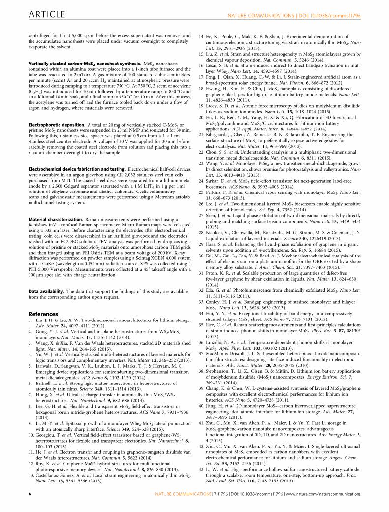
To address the effect of the C-MoS2 interface on theelectrochemical properties during lithium insertion, Ramanspectroscopy of the electrophoretically assembled MoS2-basedelectrodes at different cathodic potentials was carried out(Fig. 4b). This analysis is possible due to the preparation ofelectrodes in a manner that does not require binder materialsoften used in conventional battery electrodes that can overwhelmthe desired Raman spectroscopic features. At OCV conditions,both electrode materials exhibit only the native Raman modes ofMoS2. Cathodic scans from OCV conditions to 1.75 V versus Li/Liþ—an energy below the Liþ insertion reaction observed forvertically stacked C-MoS2 nanosheets, yields no change for thepristine MoS2 nanosheets, but the emergence of a distinct Ramanpeak at 746 cm� 1 is observed for the stacked C-MoS2 nanosheets.This mode is due to the formation of lithium polysulfides (Li2Sn
for 4rnr8) that can be attributed to chemical conversion of theMoS2 into reaction products in a manner consistent withequation (2) (ref. 44). Correspondingly, a decrease of the MoS2
a
0.8
0.8
0.4
–0.4C
urre
nt (
A g
–1)
dQ/dV
(a.
u.)
dQ/dV
(a.
u.)
Cur
rent
(A
g–1
)
–0.8
–1.2
–1.60.0 0.5 1.0 1.5
Voltage (V)2.5 3.0
3rd cycle2nd cycle1st cycle
3rd cycle2nd cycle1st cycle
2.0 0.0 0.5 1.0 1.5Voltage (V)
2.5 3.02.0
0.0 0.5 1.0 1.5Voltage (V)
2.5 3.02.00.0 0.5 1.0 1.5Voltage (V)
2.5 3.02.0
0.0
0.0
0.2
Intercalation
Conversion
0.4
0.6
0.8
1.0
0.0
0.2
0.4
0.6
0.8
1.0
0.4
–0.4
–0.8
–1.2
–1.6
0.0
c
b
d
Figure 3 | Electrochemical assessment of strained carbon-MoS2 heterostructured nanosheets. (a) CV and (b) normalized differential capacity
measurements for MoS2 under lithium insertion and extraction, with an arrow indicating the potential of the intercalation reaction that occurs in
pristine MoS2 materials. (c) CV and (d) normalized differential capacity plots for vertically stacked C-MoS2 nanosheets, with an arrow indicating the
electrochemical signature of direct chemical conversion.
ARTICLE NATURE COMMUNICATIONS | DOI: 10.1038/ncomms11796
4 NATURE COMMUNICATIONS | 7:11796 | DOI: 10.1038/ncomms11796 | www.nature.com/naturecommunications
A1g and E2g modes are observed as expected from conversion(Supplementary Fig. 8, Supplementary Note 6). This confirmsthat the high voltage B2.3 V signature in the CV and differentialcapacity curves for vertically stacked C-MoS2 nanosheets(Fig. 3c,d) is a chemical conversion process similar to that whichis known to occur at low voltages (0.55 V) in pristine MoS2. Tofurther support this, cathodic scans were continued down to0.01 V versus Li/Liþ for the pristine MoS2 electrode, where thesignature of conversion is evident due to the presence of theRaman mode at 746 cm� 1. Despite the difference in voltage ofthe conversion reactions between MoS2 and C-MoS2, similarRaman spectroscopic signatures of the polysulfide conversionproduct and similar post-conversion redox energetics in bothcases implies that the resulting chemical state of the material inboth conversion reactions is the same. To further support this, weperformed in situ electrochemical impedance spectroscopy (EIS,Supplementary Fig. 9, Supplementary Table 1), where EISanalysis was performed at the same voltages as those assessedusing Raman spectroscopy. EIS studies elucidate a pictureconsistent with Raman spectroscopy results that indicates theelectrochemical signature of conversion in different voltageregimes for the pristine MoS2 and the stacked C-MoS2,respectively (Supplementary Note 7).
DiscussionOn the basis of the combined spectroscopic and electrochemicalanalysis, a picture emerges emphasizing the role of interfacestrain on lithium insertion in vertically stacked C-MoS2 materials.In the pristine semiconducting 2H phase of MoS2, conversion ofMoS2 nanosheets cannot occur at voltages above whereintercalation occurs (1.1 V versus Li/Liþ ) and can only proceedin a two-step chemical process following an intercalationreaction. As many researchers have discussed the promise ofMoS2 nanosheets for battery cathodes, the requirement of a
conversion reaction that is near the reduction potential of lithiumis highly impractical in full-cell architectures. In a verticallystacked C-MoS2 nanosheet, the interface strain due to latticemismatch in a carbon-MoS2 solid–solid interface leads to anaverage B0.1% compressive strain that propagates into the MoS2
nanosheet lattice and enables control of the energetics of chemicalconversion. In this regard, interface strain provides theappropriate energetic landscape to sustain direct conversion atvoltages that enable pairing with conventional anode materialssuch as silicon or graphite which give promise to practicalincorporation of this device in a full-cell battery configuration.This distinctive difference in the chemical pathways achievedduring lithium insertion as a result of interface strain is illustratedin Fig. 4a, where the chemical state of the 2D materials isdrastically different following a cathodic scan to 1 V.
The broader use of controlled interface mechanics to modifychemical pathways in low-dimensional materials presents anunexplored horizon for engineered low-dimensional nanostruc-tures. This utilizes 2D materials as a framework to merge conceptsof strain engineering with mechanochemistry to control theenergetics of chemical processes relevant to energy storage, energyconversion, catalysis, and sensing applications. Building from ourresults showing that strained interfaces in vertically stackedC-MoS2 nanosheets can modulate electrochemical reactivity, weenvision a new paradigm for material design that exploits interfacestrain and mechanics as a versatile toolbox to modulateperformance of designer 2D materials in diverse applications.
MethodsMoS2 nanosheet synthesis. In all, 500 mg of bulk MoS2 powder (Aldrich, particlesizeo2 mm) was added to 50 ml of 1-methyl-2-pyrrolidinone (Aldrich, 99.5%anhydrous). The solution was sonicated in a bath sonicator for 12 h using8� 90 min intervals. After sonication, the solution was centrifuged at 2,000 r.p.m.for 40 min. The upper 2/3 of the supernatant was removed and subsequently
OCV
0.01 V
MoS2
1.75 V
Sulfur
Interface-strainedsulfur
Carbon
Molybdenum
Lithium
Lithium sulfide
aMoS2 nanosheet
Stacked (strained)MoS2 nanosheet
Intercalation Conversion
625 650 675 700Raman shift (cm–1)
Raman shift (cm–1)
Raman shift (cm–1)
725 750 775
Cou
nts
(a.u
.)C
ount
s (a
.u.)
Cou
nts
(a.u
.)
625 650 675 700 725 750 775
625 650 675 700 725 750 775
Li+ insertion
b
c
d
Mo + Li2Sn
C/(Mo + Li2Sn)
C/(Mo + Li2Sn)
C/(MoS2)
MoS2
Figure 4 | Strain-induced modulation of chemical conversion in vertically stacked C-MoS2 nanosheets. (a) Scheme showing the different chemical
states between interface-strained MoS2 nanosheets and pristine MoS2 nanosheets after Li insertion, showing chemical conversion for stacked C-MoS2 and
intercalation for pristine MoS2. Ex situ Raman spectroscopy confirming the electrochemical signature of chemical conversion based on the Raman mode of
polysulfides at 746 cm� 1 is presented for both materials at (b). Open-circuit voltage (OCV), (c) 1.75 V and (d) 0.01 V versus Li/Liþ . Notably, at 1.75 V
versus Li/Liþ , the vertically stacked C-MoS2 nanosheets have undergone chemical conversion, whereas the pristine MoS2 nanosheets remain unconverted.
NATURE COMMUNICATIONS | DOI: 10.1038/ncomms11796 ARTICLE
NATURE COMMUNICATIONS | 7:11796 | DOI: 10.1038/ncomms11796 | www.nature.com/naturecommunications 5
centrifuged for 1 h at 5,000 r.p.m. before the excess supernatant was removed andthe accumulated nanosheets were placed under vacuum overnight to completelyevaporate the solvent.
Vertically stacked carbon-MoS2 nanosheet synthesis. MoS2 nanosheetscontained within an alumina boat were placed into a 1-inch tube furnace and thetube was evacuated to 2 mTorr. A gas mixture of 100 standard cubic centimetersper minute (sccm) Ar and 20 sccm H2 maintained at atmospheric pressure wereintroduced during ramping to a temperature 750 �C. At 750 �C, 2 sccm of acetylene(C2H2) was introduced for 10 min followed by a temperature ramp to 850 �C andan additional 10 min soak, and a final ramp to 950 �C for 10 min. After this process,the acetylene was turned off and the furnace cooled back down under a flow ofargon and hydrogen, where materials were removed.
Electrophoretic deposition. A total of 20 mg of vertically stacked C-MoS2 orpristine MoS2 nanosheets were suspended in 20 ml NMP and sonicated for 30 min.Following this, a stainless steel spacer was placed at 0.5 cm from a 1� 1 cmstainless steel counter electrode. A voltage of 30 V was applied for 30 min beforecarefully removing the coated steel electrode from solution and placing this into avacuum chamber overnight to dry the sample.
Electrochemical device fabrication and testing. Electrochemical half-cell deviceswere assembled in an argon glovebox using CR 2,032 stainless steel coin cellspurchased from MTI. The coated steel discs were separated from a lithium metalanode by a 2,500 Celgard separator saturated with a 1 M LiPF6 in 1 g per 1 mlsolution of ethylene carbonate and diethyl carbonate. Cyclic voltammetryscans and galvanostatic measurements were performed using a Metrohm autolabmultichannel testing system.
Material characterization. Raman measurements were performed using aRenishaw inVia confocal Raman spectrometer. Micro-Raman maps were collectedusing a 532 nm laser. Before characterizing the electrodes after electrochemicaltesting, coin cells were disassembled in an Ar filled glovebox and the electrodeswashed with an EC/DEC solution. TEM analysis was performed by drop casting asolution of pristine or stacked MoS2 materials onto amorphous carbon TEM gridsand then imaged using an FEI Osiris TEM at a beam voltage of 200 kV. X-raydiffraction was performed on powder samples using a Scintag XGEN 4,000 systemwith a CuKa (wavelength¼ 0.154 nm) radiation source. XPS was collected using aPHI 5,000 Versaprobe. Measurements were collected at a 45� takeoff angle with a100mm spot size with charge neutralization.
Data availability. The data that support the findings of this study are availablefrom the corresponding author upon request.
References1. Liu, J. H. & Liu, X. W. Two-dimensional nanoarchitectures for lithium storage.
Adv. Mater. 24, 4097–4111 (2012).2. Gong, Y. J. et al. Vertical and in-plane heterostructures from WS2/MoS2
monolayers. Nat. Mater. 13, 1135–1142 (2014).3. Wang, X. & Xia, F. Van der Waals heterostructures: stacked 2D materials shed
light. Nat. Mater. 14, 264–265 (2015).4. Yu, W. J. et al. Vertically stacked multi-heterostructures of layered materials for
logic transistors and complementary inverters. Nat. Mater. 12, 246–252 (2013).5. Jariwala, D., Sangwan, V. K., Lauhon, L. J., Marks, T. J. & Hersam, M. C.
Emerging device applications for semiconducting two-dimensional transitionmetal dichalcogenides. ACS Nano 8, 1102–1120 (2014).
6. Britnell, L. et al. Strong light-matter interactions in heterostructures ofatomically thin films. Science 340, 1311–1314 (2013).
7. Hong, X. et al. Ultrafast charge transfer in atomically thin MoS2/WS2
heterostructures. Nat. Nanotechnol. 9, 682–686 (2014).8. Lee, G.-H. et al. Flexible and transparent MoS2 field-effect transistors on
hexagonal boron nitride-graphene heterostructures. ACS Nano 7, 7931–7936(2013).
9. Li, M.-Y. et al. Epitaxial growth of a monolayer WSe2-MoS2 lateral pn junctionwith an atomically sharp interface. Science 349, 524–528 (2015).
10. Georgiou, T. et al. Vertical field-effect transistor based on graphene-WS2
heterostructures for flexible and transparent electronics. Nat. Nanotechnol. 8,100–103 (2013).
11. He, J. et al. Electron transfer and coupling in graphene–tungsten disulfide vander Waals heterostructures. Nat. Commun. 5, 5622 (2014).
12. Roy, K. et al. Graphene-MoS2 hybrid structures for multifunctionalphotoresponsive memory devices. Nat. Nanotechnol. 8, 826–830 (2013).
13. Castellanos-Gomez, A. et al. Local strain engineering in atomically thin MoS2.Nano Lett. 13, 5361–5366 (2013).
14. He, K., Poole, C., Mak, K. F. & Shan, J. Experimental demonstration ofcontinuous electronic structure tuning via strain in atomically thin MoS2. NanoLett. 13, 2931–2936 (2013).
15. Liu, Z. et al. Strain and structure heterogeneity in MoS2 atomic layers grown bychemical vapour deposition. Nat. Commun. 5, 5246 (2014).
16. Desai, S. B. et al. Strain-induced indirect to direct bandgap transition in multilayer WSe2. Nano Lett. 14, 4592–4597 (2014).
17. Feng, J., Qian, X., Huang, C.-W. & Li, J. Strain-engineered artificial atom as abroad-spectrum solar energy funnel. Nat. Photon. 6, 866–872 (2012).
18. Hwang, H., Kim, H. & Cho, J. MoS2 nanoplates consisting of disorderedgraphene-like layers for high rate lithium battery anode materials. Nano Lett.11, 4826–4830 (2011).
19. Lacey, S. D. et al. Atomic force microscopy studies on molybdenum disulfideflakes as sodium-ion anodes. Nano Lett. 15, 1018–1024 (2015).
20. Hu, L. R., Ren, Y. M., Yang, H. X. & Xu, Q. Fabrication of 3D hierarchicalMoS2/polyaniline and MoS2/C architectures for lithium-ion batteryapplications. ACS Appl. Mater. Inter. 6, 14644–14652 (2014).
21. Kibsgaard, J., Chen, Z., Reinecke, B. N. & Jaramillo, T. F. Engineering thesurface structure of MoS2 to preferentially expose active edge sites forelectrocatalysis. Nat. Mater. 11, 963–969 (2012).
22. Chou, S. S. et al. Understanding catalysis in a multiphasic two-dimensionaltransition metal dichalcogenide. Nat. Commun. 6, 8311 (2015).
23. Wang, Y. et al. Monolayer PtSe2, a new transition-metal-dichalcogenide, grownby direct selenization, shows promise for photocatalysis and valleytronics. NanoLett. 15, 4013–4018 (2015).
24. Sarkar, D. et al. MoS2 field-effect transistor for next-generation label-freebiosensors. ACS Nano. 8, 3992–4003 (2014).
25. Perkins, F. K. et al. Chemical vapor sensing with monolayer MoS2. Nano Lett.13, 668–673 (2013).
26. Lee, J. et al. Two-dimensional layered MoS2 biosensors enable highly sensitivedetection of biomolecules. Sci. Rep. 4, 7352 (2014).
27. Shen, J. et al. Liquid phase exfoliation of two-dimensional materials by directlyprobing and matching surface tension components. Nano Lett. 15, 5449–5454(2015).
28. Nicolosi, V., Chhowalla, M., Kanatzidis, M. G., Strano, M. S. & Coleman, J. N.Liquid exfoliation of layered materials. Science 340, 1226419 (2013).
29. Haar, S. et al. Enhancing the liquid-phase exfoliation of graphene in organicsolvents upon addition of n-octylbenzene. Sci. Rep. 5, 16684 (2015).
30. Du, M., Cui, L., Cao, Y. & Bard, A. J. Mechanoelectrochemical catalysis of theeffect of elastic strain on a platinum nanofilm for the ORR exerted by a shapememory alloy substrate. J. Amer. Chem. Soc. 23, 7397–7403 (2015).
31. Paton, K. R. et al. Scalable production of large quantities of defect-freefew-layer graphene by shear exfoliation in liquids. Nat. Mater. 13, 624–630(2014).
32. Eda, G. et al. Photoluminescence from chemically exfoliated MoS2. Nano Lett.11, 5111–5116 (2011).
33. Conley, H. J. et al. Bandgap engineering of strained monolayer and bilayerMoS2. Nano Lett. 13, 3626–3630 (2013).
34. Hui, Y. Y. et al. Exceptional tunability of band energy in a compressivelystrained trilayer MoS2 sheet. ACS Nano 7, 7126–7131 (2013).
35. Rice, C. et al. Raman-scattering measurements and first-principles calculationsof strain-induced phonon shifts in monolayer MoS2. Phys. Rev. B. 87, 081307(2013).
36. Lanzillo, N. A. et al. Temperature-dependent phonon shifts in monolayerMoS2. Appl. Phys. Lett. 103, 093102 (2013).
37. MacManus-Driscoll, J. L. Self-assembled heteroepitaxial oxide nanocompositethin film structures: designing interface-induced functionality in electronicmaterials. Adv. Funct. Mater. 20, 2035–2045 (2010).
38. Stephenson, T., Li, Z., Olsen, B. & Mitlin, D. Lithium ion battery applicationsof molybdenum disulfide (MoS2) nanocomposites. Energy Environ. Sci. 7,209–231 (2014).
39. Chang, K. & Chen, W. L-cysteine-assisted synthesis of layered MoS2/graphenecomposites with excellent electrochemical performances for lithium ionbatteries. ACS Nano 5, 4720–4728 (2011).
40. Jiang, H. et al. 2D monolayer MoS2–carbon interoverlapped superstructure:engineering ideal atomic interface for lithium ion storage. Adv. Mater. 27,3687–3695 (2015).
41. Zhu, C., Mu, X., van Aken, P. A., Maier, J. & Yu, Y. Fast Li storage inMoS2-graphene-carbon nanotube nanocomposites: advantageousfunctional integration of 0D, 1D, and 2D nanostructures. Adv. Energy Mater. 5,4 (2015).
42. Zhu, C., Mu, X., van Aken, P. A., Yu, Y. & Maier, J. Single-layered ultrasmallnanoplates of MoS2 embedded in carbon nanofibers with excellentelectrochemical performance for lithium and sodium storage. Angew. Chem.Int. Ed. 53, 2152–2156 (2014).
43. Li, W. et al. High-performance hollow sulfur nanostructured battery cathodethrough a scalable, room temperature, one-step, bottom-up approach. Proc.Natl Acad. Sci. USA 110, 7148–7153 (2013).
ARTICLE NATURE COMMUNICATIONS | DOI: 10.1038/ncomms11796
6 NATURE COMMUNICATIONS | 7:11796 | DOI: 10.1038/ncomms11796 | www.nature.com/naturecommunications
44. Yeon, J.-T. et al. Raman spectroscopic and X-ray diffraction studies of sulfurcomposite electrodes during discharge and charge. J. Electrochem. Soc. 159,A1308–A1314 (2012).
AcknowledgementsWe thank Nitin Muralidharan and Professor Rizia Bardhan for insightful discussions.This work was supported by the National Science Foundation under CMMI grant#1334269 and Vanderbilt start-up funds. TEM images were obtained from an instrumentmade possible by NSF grant EPS 1004083. A.P.C. and K.S. are supported by an NSFgraduate fellowship under grant # 1445197.
Author contributionsL.O. and C.L.P jointly conceived the project and designed the experiments. L.O. and T.H.performed material fabrication with insights from K.S., and L.O. carried out devicetesting and performance analysis. R.C. performed TEM imaging and analysis, and A.P.C.performed X-ray diffraction measurements and analysis. B.S. performed XPSmeasurements and analysis. L.O. and C.L.P. wrote the manuscript and all authorsparticipated in discussion and reviewed the manuscript before submission.
Additional informationSupplementary Information accompanies this paper at http://www.nature.com/naturecommunications
Competing financial interests: The authors declare no competing financial interests.
Reprints and permission information is available online at http://npg.nature.com/reprintsandpermissions/
How to cite this article: Oakes, L. et al. Interface strain in vertically stackedtwo-dimensional heterostructured carbon-MoS2 nanosheets controlselectrochemical reactivity. Nat. Commun. 7:11796 doi: 10.1038/ncomms11796(2016).
This work is licensed under a Creative Commons Attribution 4.0International License. The images or other third party material in this
article are included in the article’s Creative Commons license, unless indicated otherwisein the credit line; if the material is not included under the Creative Commons license,users will need to obtain permission from the license holder to reproduce the material.To view a copy of this license, visit http://creativecommons.org/licenses/by/4.0/
NATURE COMMUNICATIONS | DOI: 10.1038/ncomms11796 ARTICLE
NATURE COMMUNICATIONS | 7:11796 | DOI: 10.1038/ncomms11796 | www.nature.com/naturecommunications 7


![WordPress.comLeft indent; [C] Wrap text anentation:: O deg rees C] Vertically stacked E] Appearance Cell background: 13 Items Cake Pa r lates Sweets Saloons Party Expense Quantity](https://img.pdfslide.us/doc/110x75/604f20606ff8db52897e6794/left-indent-c-wrap-text-anentation-o-deg-rees-c-vertically-stacked-e-appearance.jpg)

![Transport in vertically stacked hetero-structures from 2D ... · TFET designs exploiting di erent 2D material properties[5{11] have been proposed to increase the tunneling current](https://img.pdfslide.us/doc/110x75/606ad5102efe0335090e5c64/transport-in-vertically-stacked-hetero-structures-from-2d-tfet-designs-exploiting.jpg)