Embed Size (px)
Citation preview

Interconnect Materials in
Electronic Packaging
Kwang-Lung Lin
Student Program, IEEE CPMT

Consumers’ Electronics-IC chips are packaged
2015 2

Electronics Buffet – All-in-One
Function Integration
2015
source: 3D ICs-SEMICON Taiwan 2009
3

Notebook –packaged components
2015
Flip Chip BGA
PGA
BGA
4

Various Levels of Electronic
Packaging
Die level Module level
Substrate/Board
level
System level
2015 5

Multilayer Ceramic PGA (wire
bonded)
Wire Bond
Si Si
2015 6

ACF TAB
Flip Chip Wire Bond
Interconnect – Die Level
2015 7

Die Level Interconnect – Wire Bond D. P. Seraphim et al., “Principles of Electronic Packaging”, McGraw-Hill, 1993
2015
Ball Bond
Wedge Bond
chip-terminal-to-wire
interconnection
wire-to-chip carrier
interconnection
8

Wire Bonding ProcessH. Xu/Scripta Materialia 61 (2009) 165–168
C.J. Hang / Microelectronic Engineering 85 (2008) 1815–1819, “Microstructural study of copper free air
balls in thermosonic wire bonding”
2015
(a)Electric flame-off
(EFO) process to
produce a spherical
ball
(c)transverse ultrasonic vibration
(150 mW); 0.025sec
(b)Al pad (1 um
thick); heat (200oC).
(c)Normal force
(0.6 N)
Wedge Bond
Ball Bond
9

2015
Cu Wire Ball BondIvy Qin,, Hui Xu, Horst Clauberg, Ray Cathcart, Viola L. Acoff, Bob Chylak, and Cuong Huynh,
2011 Electronic Components and Technology Conference, 1489
Al pad
splashCu wireCu wire
Si
10

Terminal Metallization Materials
for Wire Bonding
On Si
Al, Cu doped Al
On Lead (e.g., Cu alloy, Fe-Ni alloy) and
Carrier
Pd-Ag
Au-Pd
Ni
2015 11

Material Criteria for Bonding
Wire
drawability into fine wire
strength for wire handling
feasible with bonding techniques
ductility for plastic deformation during
bonding
high electrical conductivity
corrosion resistance
2015 12

2015
Wire Bonding Materials
0.8 mil ~ 0.6 mil (moving finer) diameter
Au, Au-Be
Au-Be alloys: e.g.,1~2% or 30~100ppm Be to
inhibit grain growth, increase yield
Cu, Pd plated Cu
Pd plating to prevent Cu from oxidation
Ag, Ag-Pd, Pd (100nm)plated Ag(2N)
96~97% Ag + Pd to enhance mechanical
strength and oxidation resistance.13

Pd Plated Cu WireIvy Qin,, Hui Xu, Horst Clauberg, Ray Cathcart, Viola L. Acoff, Bob Chylak, and Cuong Huynh,
2011 Electronic Components and Technology Conference, 1489
2015
50 nm
14

IMC formed in Cu Wire Bonding on Al
Y. H. Lu, Y. W. Wang, B. K. Appelt, Y. S. Lai, and C. R. Kao, 2011 Electronic Components and
Technology Conference,1481
Secure Bonding Strength
2015 15

2015
Wire Bonding Interaction
Ag-Al Inerconnection
Formation of AgAl2
Au-Al Interconnection
Formation of intermetallics (IMC):
Au5Al2, Au2Al, AuAl2, AuAl, Au4Al
Cu-Al Interconnection
Formation of IMC:
CuAl, Cu2Al, Cu9Al4
16

2015
•Electronegativity:
XAu > XCu ; Chemical Affinity for Al: Au > Cu
•Atomic size difference:•∆r (Al-Au) < ∆r (Al-Cu)
the larger size difference between Al and Cu
the lower electronegativity of Cu
hinder Al solubility in Cu
Au and Cu Wire BondingS. Murali et al., Materials Research Bulletin 38 (2003) 637–646
17

2015
Wire Material Comparison:
Au vs. CuS. Murali et al., Materials Research Bulletin 38 (2003) 637–646
Enthalpy of formation of intermetallic compound: (J.H. Westbrook, R.L. Fleischer, Intermetallic Compounds 1 (1994) 91–125, 227–275.)
Z: number of valence bonds
XA, XB: electronegativity of elements A and B
∆H (Al-Au) > ∆H (Al-Cu)
18
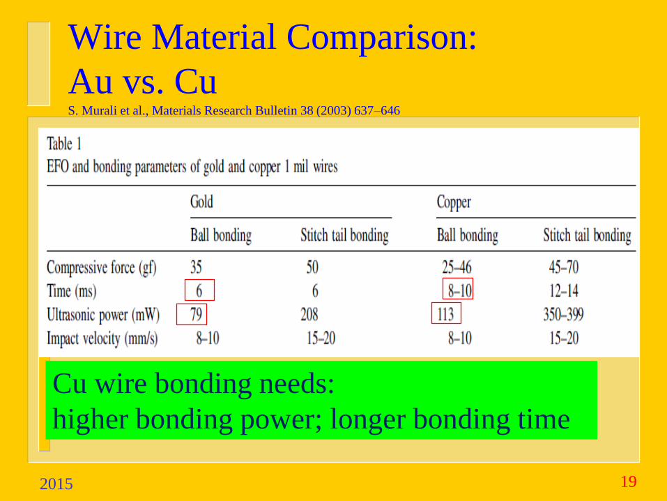
Wire Material Comparison:
Au vs. CuS. Murali et al., Materials Research Bulletin 38 (2003) 637–646
2015
Cu wire bonding needs:
higher bonding power; longer bonding time
19

Flip Chip
Wire Bond
Interconnect – Die Level
2015
Bumping Bonding
Wedge BondBall Bond
20

Solder Bump
UBM
(Under Bump
Metal)
Solder
Si
2015 21

222015
Flip Chip Solder Bump
Chip
Chip passivation
Al or Cu pad
Solder
bump
Oxidation barrier
layer
Wetting layer
Adhesion/barrier
layer
Chip
Substrate
Top side
metallurgy(TSM)

Bumping Process (1/2) –
Ti/Cu UBM
2015 23

Bumping Process (2/2) –
Ti/Cu UBM
2015 24

2015
Electroplated Solder Bump
Reflow
25

IMC formed between Solder and
Electroless Nickel Barrier Layer
C. Y. Lee and K. L. Lin, "The Interaction Kinetics and Compound Formation
Between Electroless Ni-P and Solder," Thin Solid Films, 249, (1994) 201-206.
2015 26

Flip Chip Bonding vs.
Wire Bonding
Flip Chip -
Bonding is performed
at once, a gang
bonding process
Wire Bonding-
Bonding is performed
one by one individually
2015 27

Module Level Interconnect
– Leaded and Leadless
2015
BGA
SMT Surface Mount Technology
Through Hole Technology
Ball Grid Array
THT
Leaded
Leadless
28

2015
THT – Wave Soldering
29

2015
SMT Component - Pick and PlaceR. J. K. Wassink, “Soldering in Electronics”, 2nd edn.
Solder PastePick and Place
30

Screen Printing of Solder Paste
2015
SMT Magazine • August 2011
R. J. K. Wassink, “Soldering in Electronics”, 2nd
edn.
31

2015
BGA Substrate/Solder Ball
Die pad Ball pad
solder ball
SMT Magazine • May 2011
Ball size: 300 ~ 760 µm
solder
ball
bonded
32

Notebook –packaged components
2015
Flip BGA
PGA
BGA
33

Solder Products (the form of solder)
for Electronics Manufacturing
Solder bump
Solder preform
Solder powder
Solder paste
Solder powder + flux
Solder ball
Solder wire
Solder ingot
2015 34

2015
Action of Flux and Soldering OccurrenceR. J. K. Wassink, “Soldering in Electronics” 2nd edn.
Enhance wetting through:
Clean tarnish film on substrate (e.g., CuO)
Clean tarnish film on solder powder (e.g., SnO)
Lower surface tension of solder and substrate (air to flux
atmosphere)
35

2015
Sn-Pb Phase Diagram
Sn-Pb Phase Diagram
Pb: (prohibited by WEEE, RoHS)
Low price
Enhance oxidation resistance
Lower surface tension
470 dyne/cm for 63Sn-37Pb at 230oC, 550 dyne/cm for Sn at 232oC
Eutectic with Sn
Toxic
Eutectic 183oC
36
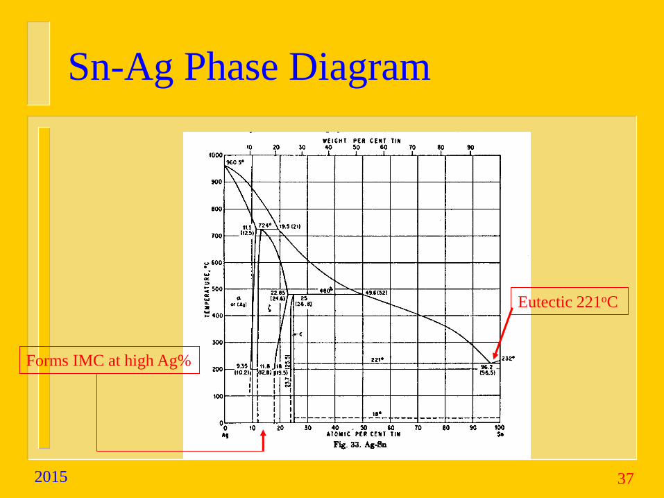
2015
Sn-Ag Phase Diagram
Forms IMC at high Ag%
Eutectic 221oC
37

2015
Sn-Cu Phase Diagram
Eutectic 227oC
Forms IMC
38

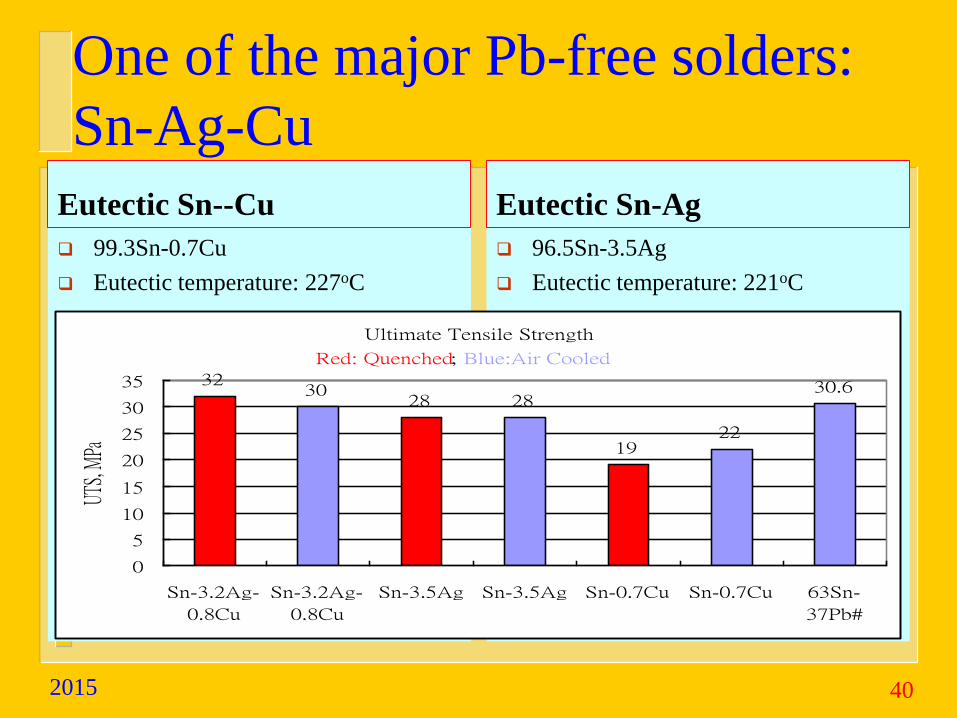
One of the major Pb-free solders:
Sn-Ag-Cu
99.3Sn-0.7Cu
Eutectic temperature: 227oC
96.5Sn-3.5Ag
Eutectic temperature: 221oC
2015
1413 13 13
11.9
101112131415
Sn-3.5Ag Sn-3.5Ag-0.7Cu Sn-3.8Ag-0.7Cu Sn-0.7Cu Sn-37Pb
Ele
ctr
ical
Co
nd
uc
tiv
it
y,
%IA
CS
Eutectic Sn-AgEutectic Sn--Cu
39
One of the major Pb-free solders:
Sn-Ag-Cu
99.3Sn-0.7Cu
Eutectic temperature: 227oC
96.5Sn-3.5Ag
Eutectic temperature: 221oC
2015
Ultimate Tensile Strength
3230
28 28
1922
30.6
0
5
10
15
20
25
30
35
Sn-3.2Ag-
0.8Cu
Sn-3.2Ag-
0.8Cu
Sn-3.5Ag Sn-3.5Ag Sn-0.7Cu Sn-0.7Cu 63Sn-
37Pb#
UTS,
MPa
Red: Quenched; Blue:Air Cooled
Eutectic Sn--Cu Eutectic Sn-Ag
40
2015
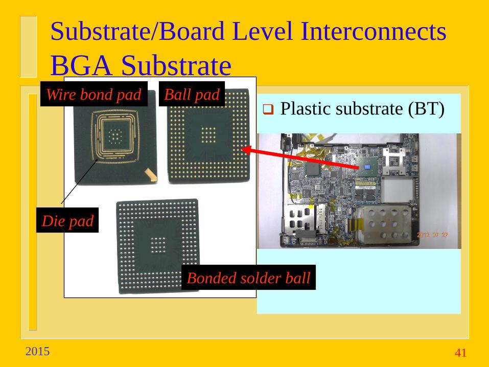
Substrate/Board Level Interconnects
BGA Substrate
Plastic substrate (BT)
Die pad
Wire bond pad Ball pad
Bonded solder ball
41

42
Metallization on BGA Substrate
Contact Material
Barrier Material
Base Material
(Cu circuit)
Au
Ni
Cu
Cu
OSP
Organic solder preservative
2015

43
3-D Sketch of PC Boardsource: Principle of Electronic Packaging, C. Li
2015

44
Plated Through HoleWassink, Soldering in Electronics
Glass fiber
25 μm Cu plating
Through
Hole
Through Hole
Circuits
Cu plating
(0.8mm)
2015

45
Through-Hole Activation (Electroless
Cu Deposition) source: Principle of Electronic Packaging, C. Li
The electroless Cu provides the
conducting base for electroplating.
2015

Integration of Interconnects in
Electronic Packaging
2015 46

Integration of Interconnect Technology
and Material – Stacked/3D IC PackagingM. Kada and L.Smith, PanPacific Microelecronics Symposium Conference, Jan. 2000
472015

3D Packaging
2015 48
source: 3D Packaging, Issue No. 23, May 2012 source: 3D Packaging, Issue No. 22, February 2012
http://www.infoneedle.com/category/tags/wide-
i/o?snc=20641 source: SEMICON Taiwan, 2009