Embed Size (px)
Citation preview

Freescale Semiconductor Document Number: MMA955xLData Sheet: Advance Information Rev. 1, 10/2011An Energy Efficient Solution by Freescale
This document contains information on a new product. Specifications and information herein are subject to change without notice.
© 2011 Freescale Semiconductor, Inc. All rights reserved.
Intelligent Motion-Sensing PlatformThe MMA955xL device is a member of Freescale’s Xtrinsic family of intelligent sensor platforms. This device incorporates dedicated accelerometer MEMS transducers, signal conditioning, data conversion, and a 32-bit programmable microcontroller.This unique blend transforms Freescale’s MMA955xL into an intelligent, high-precision, motion-sensing platform able to manage multiple sensor inputs. This device can make system-level decisions required for sophisticated applications such as gesture recognition, pedometer functionality, tilt compensation and calibration, and activity monitoring.The MMA955xL device is programmed and configured with the CodeWarrior Development Studio for Microcontrollers software, version 10.1 or later. This standard integrated design environment enables customers to quickly implement custom algorithms and features to exactly match their application needs.Using the master I2C port, the MMA955xL device can manage secondary sensors, such as pressure sensors, magnetometers, or gyroscopes. This allows sensor initialization, calibration, data compensation, and computation functions to be off-loaded from the system application processor. The MMA955xL device also acts as an intelligent sensing hub and a highly configurable decision engine. Total system power consumption is significantly reduced because the application processor stays powered down until absolutely needed.
Hardware Features• Three accelerometer operating ranges:
– ±2g suits most hand gestures (orientation detection and tit control) and freefall. For tap detection, ±4g and ±8g are supported.
– ±4g covers most regular human dynamics (walking and jogging)– ±8g detects most abrupt activities (gaming)
• Integrated temperature sensor• One slave SPI or I2C interface operating at up to 2 Mbps, dedicated to
communication with host processor. Default value of the I2C, 7-bit address is 0x4C. (This can be customized by firmware.)
• One master I2C interface operating at up to 400 kbps that can be used to communicate with external sensors
• Eight selectable output data rates (ODR), from 488 Hz to 3.8 Hz• 10, 12, 14, and 16-bit trimmed ADC data formats available• 1.8V supply voltage• 32-bit ColdFire V1 CPU with MAC unit• Extensive set of power-management features and low-power modes• Integrated ADC can be used to convert external analog signals• Single-Wire, Background-Debug Mode (BDM) pin interface• 16-KB flash memory• 2-KB Random Access Memory• ROM-based flash controller and slave-port, command-line interpreter• Two-channel timer with input capture, output capture, or edge-aligned PWM• Programmable delay block for scheduling events relative to start of frame• A 16-bit, modulo timer for scheduling periodic events• Minimal external component requirements• RoHS compliant (-40 to +85ºC), 16-pin, 3 x 3 x 1-mm LGA package
16-pin LGA3 mm x 3 mm x 1 mm
Case 2094-01
MMA955xL
Top and bottom view
Top view
Pin connections
1
2
3
4
56 7 8
9
13
12
11
10
16 15 14VDD
RGPIO7/AN1/TPMCH1
RG
PIO
8/P
DB_
B
SD
A0/
RG
PIO
1/SD
I
BKGD-MS/RGPIO9RESETB
SCL0/RGPIO0SCLK
VSS
RG
PIO
2/S
CL1
/SD
O
RG
PIO
3/S
DA
1/S
SB
RGPIO6/AN0TPMCH0RGPIO5/PDB_A/INT_OVSS
RGPIO4/INT
VD
DA
V SS
A
MMA955xL
Sensors2 Freescale Semiconductor, Inc.
Software FeaturesThis device can be programmed to provide any of the following:
• Orientation detection (portrait/landscape)• High-g/Low-g threshold detection• Pulse detection (single, double and directional tap)• Tilt detection• Auto wake/sleep• Embedded, smart FIFO• Power management• Pedometer
A selection of the software features are included in the factory-programmed firmware for some devices. Users may add their own features with user firmware.The power and flexibility of the embedded ColdFire V1 MCU core has new and unprecedented capabilities.
Table 1. Ordering informationPart number Firmware Temperature range Package description Shipping
MMA9550LT Motion -40°C to +85°C LGA-16 Tray
MMA9550LR1 Motion -40°C to +85°C LGA-16 Tape and reel
MMA9551LT Gesture -40°C to +85°C LGA-16 Tray
MMA9551LR1 Gesture -40°C to +85°C LGA-16 Tape and reel
MMA9553LR1 Pedometer -40°C to +85°C LGA-16 Tape and reel
MMA 9559LR1 Foundation -40°C to +85°C LGA-16 Tape and reel

MMA955xL
Sensors3 Freescale Semiconductor, Inc.
Related DocumentationThe MMA955xL device features and operations are described in a variety of reference manuals, user guides, and application notes. To find the most-current versions of these documents:
1. Go to the Freescale homepage at:http://www.freescale.com/
2. In the Keyword search box at the top of the page, enter the device number MMA955xL.3. In the Refine Your Result pane on the left, click on the Documentation link.
Contents1 Variations of MMA955xL Device . . . . . . . . . . . . . . . . . . . . . . . . . . . . . . . . . . . . . . . . . . . . . . . . . . . . . . . . . . . . . . . . . . . . 42 Typical Applications. . . . . . . . . . . . . . . . . . . . . . . . . . . . . . . . . . . . . . . . . . . . . . . . . . . . . . . . . . . . . . . . . . . . . . . . . . . . . . 63 General Description . . . . . . . . . . . . . . . . . . . . . . . . . . . . . . . . . . . . . . . . . . . . . . . . . . . . . . . . . . . . . . . . . . . . . . . . . . . . . . 7
3.1. . Functional Overview . . . . . . . . . . . . . . . . . . . . . . . . . . . . . . . . . . . . . . . . . . . . . . . . . . . . . . . . . . . . . . . . . . . . . . . . . . 73.2. . Packaging Information . . . . . . . . . . . . . . . . . . . . . . . . . . . . . . . . . . . . . . . . . . . . . . . . . . . . . . . . . . . . . . . . . . . . . . . . 8
3.2.1 Package diagrams. . . . . . . . . . . . . . . . . . . . . . . . . . . . . . . . . . . . . . . . . . . . . . . . . . . . . . . . . . . . . . . . . . . . . . 83.2.2 Sensing Direction and Output Response . . . . . . . . . . . . . . . . . . . . . . . . . . . . . . . . . . . . . . . . . . . . . . . . . . . 113.2.3 Pin Functions. . . . . . . . . . . . . . . . . . . . . . . . . . . . . . . . . . . . . . . . . . . . . . . . . . . . . . . . . . . . . . . . . . . . . . . . . 11
3.3. . Pin Function Descriptions. . . . . . . . . . . . . . . . . . . . . . . . . . . . . . . . . . . . . . . . . . . . . . . . . . . . . . . . . . . . . . . . . . . . . 123.4. . System Connections. . . . . . . . . . . . . . . . . . . . . . . . . . . . . . . . . . . . . . . . . . . . . . . . . . . . . . . . . . . . . . . . . . . . . . . . . 12
3.4.1 Power Sequencing . . . . . . . . . . . . . . . . . . . . . . . . . . . . . . . . . . . . . . . . . . . . . . . . . . . . . . . . . . . . . . . . . . . . 123.4.2 Layout Recommendations. . . . . . . . . . . . . . . . . . . . . . . . . . . . . . . . . . . . . . . . . . . . . . . . . . . . . . . . . . . . . . . 123.4.3 MMA955xL Platform as an Intelligent Slave . . . . . . . . . . . . . . . . . . . . . . . . . . . . . . . . . . . . . . . . . . . . . . . . . 133.4.4 MMA955xL Platform as a Sensor Hub . . . . . . . . . . . . . . . . . . . . . . . . . . . . . . . . . . . . . . . . . . . . . . . . . . . . . 15
4 Mechanical and Electrical Specifications. . . . . . . . . . . . . . . . . . . . . . . . . . . . . . . . . . . . . . . . . . . . . . . . . . . . . . . . . . . . 164.1. . Definitions. . . . . . . . . . . . . . . . . . . . . . . . . . . . . . . . . . . . . . . . . . . . . . . . . . . . . . . . . . . . . . . . . . . . . . . . . . . . . . . . . 164.2. . Pin Groups . . . . . . . . . . . . . . . . . . . . . . . . . . . . . . . . . . . . . . . . . . . . . . . . . . . . . . . . . . . . . . . . . . . . . . . . . . . . . . . . 164.3. . Absolute Maximum Ratings . . . . . . . . . . . . . . . . . . . . . . . . . . . . . . . . . . . . . . . . . . . . . . . . . . . . . . . . . . . . . . . . . . . 164.4. . Operating Conditions . . . . . . . . . . . . . . . . . . . . . . . . . . . . . . . . . . . . . . . . . . . . . . . . . . . . . . . . . . . . . . . . . . . . . . . . 174.5. . Electrostatic Discharge (ESD) and Latch-up Protection Characteristics . . . . . . . . . . . . . . . . . . . . . . . . . . . . . . . . . 174.6. . General DC Characteristics . . . . . . . . . . . . . . . . . . . . . . . . . . . . . . . . . . . . . . . . . . . . . . . . . . . . . . . . . . . . . . . . . . . 174.7. . Supply Current Characteristics. . . . . . . . . . . . . . . . . . . . . . . . . . . . . . . . . . . . . . . . . . . . . . . . . . . . . . . . . . . . . . . . . 184.8. . Accelerometer Transducer Mechanical Characteristics . . . . . . . . . . . . . . . . . . . . . . . . . . . . . . . . . . . . . . . . . . . . . . 184.9. . Temperature Sensor Characteristics . . . . . . . . . . . . . . . . . . . . . . . . . . . . . . . . . . . . . . . . . . . . . . . . . . . . . . . . . . . . 194.10. ADC Characteristics . . . . . . . . . . . . . . . . . . . . . . . . . . . . . . . . . . . . . . . . . . . . . . . . . . . . . . . . . . . . . . . . . . . . . . . . . 194.11. ADC Sample Rates . . . . . . . . . . . . . . . . . . . . . . . . . . . . . . . . . . . . . . . . . . . . . . . . . . . . . . . . . . . . . . . . . . . . . . . . . 194.12. AC Electrical Characteristics . . . . . . . . . . . . . . . . . . . . . . . . . . . . . . . . . . . . . . . . . . . . . . . . . . . . . . . . . . . . . . . . . . 204.13. General Timing Control . . . . . . . . . . . . . . . . . . . . . . . . . . . . . . . . . . . . . . . . . . . . . . . . . . . . . . . . . . . . . . . . . . . . . . 204.14. I2C Timing. . . . . . . . . . . . . . . . . . . . . . . . . . . . . . . . . . . . . . . . . . . . . . . . . . . . . . . . . . . . . . . . . . . . . . . . . . . . . . . . . 21
4.14.1 Slave I2C . . . . . . . . . . . . . . . . . . . . . . . . . . . . . . . . . . . . . . . . . . . . . . . . . . . . . . . . . . . . . . . . . . . . . . . . . . . . 214.14.2 Master I2C Timing . . . . . . . . . . . . . . . . . . . . . . . . . . . . . . . . . . . . . . . . . . . . . . . . . . . . . . . . . . . . . . . . . . . . . 21
4.15. Slave SPI Timing . . . . . . . . . . . . . . . . . . . . . . . . . . . . . . . . . . . . . . . . . . . . . . . . . . . . . . . . . . . . . . . . . . . . . . . . . . . 224.16. Flash Parameters . . . . . . . . . . . . . . . . . . . . . . . . . . . . . . . . . . . . . . . . . . . . . . . . . . . . . . . . . . . . . . . . . . . . . . . . . . . 23
5 Package Information . . . . . . . . . . . . . . . . . . . . . . . . . . . . . . . . . . . . . . . . . . . . . . . . . . . . . . . . . . . . . . . . . . . . . . . . . . . . 236 Revision History . . . . . . . . . . . . . . . . . . . . . . . . . . . . . . . . . . . . . . . . . . . . . . . . . . . . . . . . . . . . . . . . . . . . . . . . . . . . . . . . 24

MMA955xL
Sensors4 Freescale Semiconductor, Inc.
1 Variations of MMA955xL DeviceFreescale offers a variety of firmware versions for the MMA955xL devices. The different versions of the device are identified by the fourth digit in the part number (for example MMA9559). Information and specifications provided in this data sheet are inde-pendent of the Freescale firmware versions.
The following table lists some of the variations among the MMA955xL-platform devices.
Table 2. Features of product-line devices
Feature - Device MMA9550L MMA9551L MMA9553 MMA9559L
Key elements Motion sensing Gesture sensing Pedometer High flexibility
User flash available 6.5 KB 4.5 KB 1.5K 14 KB
User RAM available 576 bytes 452 bytes 200 bytes 1664 bytes
Digital resolution (bits) 10,12,14,16 bits 10,12,14,16 bits 10,12,14,16 bits 10,12,14,16 bits
G measurement ranges 2g, 4g, 8g 2g, 4g, 8g 2g, 4g, 8g 2g, 4g, 8g
Real-time and preemptive scheduling Yes Yes Yes No
Event management No No No Yes
Slave Port Command Interpreter
• Normal mode Yes Yes Yes No
• Legacy mode Yes Yes Yes No
• Streaming mode Yes Yes Yes No
Front-end processing
• 100-Hz BW anti-aliasing Yes Yes Yes No
• 50-Hz BW anti-aliasing Yes Yes Yes No
• g-mode-dependent resolution Yes Yes Yes Yes
• Absolute value Yes Yes Yes No
• Low-pass filter Yes Yes Yes No
• High-pass filter Yes Yes Yes No
• Data-ready interrupt Yes Yes Yes Yes
Gesture applications
• High g/Low g No Yes No No
• Tilt No Yes No No
• Portrait/Landscape No Yes No No
• Programmable orientation No Yes No No
• Tap/Double-tap No Yes No No
• Freefall No Yes No No
• Motion No Yes No No

MMA955xL
SensorsFreescale Semiconductor, Inc. 5
The only difference between the various device configurations is the firmware content that is loaded into the flash memory at the factory. The user still can add custom software using the remaining portion of flash memory.
The MMA9550, MMA95501, and MMA95503 devices can function immediately as they are. They have an internal command interpreter and applications scheduler and can interact directly with the users’ host system.
The MMA9559 device provides the most flexibility and is for users who need to design their own control loop and system. The device needs to be programmed with custom user code.
Data-storage modules
• Data FIFO Yes Yes Yes No
• Event queue Yes Yes Yes No
• Inter-process FIFO No No No Yes
Power-control module
• Run and Stop on idle Yes Yes Yes Yes
• Run and No stop Yes Yes Yes Yes
• Stop NC Yes Yes Yes Yes
• Auto-Wake / Auto-Sleep / Doze Yes Yes Yes No
Data-management daemons Yes Yes Yes
Pedometer applications
• Step count No No Yes No
• Distance No No Yes No
• Adaptive distance No No Yes No
• Activity monitor No No Yes No
Table 2. Features of product-line devices (Continued)
Feature - Device MMA9550L MMA9551L MMA9553 MMA9559L

MMA955xL
Sensors6 Freescale Semiconductor, Inc.
2 Typical ApplicationsThis low-power, intelligent sensor platform is optimized for use in portable and mobile consumer products such as:
• Mobile phones/PMP/PDA/digital cameras– Orientation detection (portrait/landscape)– Image stability– Tilt control enabled with higher resolution– Gesture recognition– Tap to control– Auto wake/sleep for low power consumption
• Smartbooks/ereaders/netbooks/laptops– Anti-theft– Freefall detection for hard-disk drives– Orientation detection– Tap detection
• Pedometers• Gaming and toys• Activity monitoring in medical applications• Security
– Anti-theft– Shock detection– Tilt
• Fleet monitoring, tracking– Dead reckoning– System auto-wake on movement– Detection– Shock recording– Anti-theft
• Power tools and small appliances– Tilt– Safety shut-off

MMA955xL
SensorsFreescale Semiconductor, Inc. 7
3 General Description3.1 Functional OverviewThe MMA955xL device consists of a 3-axis, MEMS accelerometer and a mixed-signal ASIC with an integrated, 32-bit CPU. The mixed-signal ASIC can be utilized to measure and condition the outputs of the MEMS accelerometer, internal temperature sensor, or a differential analog signal from an external device.
These measured values can be read via the slave I2C or SPI port or utilized internally within the MMA955xL platform.
Figure 1. Platform block diagram(1)
1. Preliminary data for memory sizes.
A block level view of is shown in the preceding figure and can be summarized at a high level as an analog/mixed-mode subsystem associated with a digital engine:
• The analog sub-system is composed of:– A 3-axis transducer that is an entirely passive block including the MEMS structures.– An Analog Front End (AFE) with the following:
• A capacitance-to-voltage converter (C to V)• An analog-to-digital converter• A temperature sensor
• The digital sub-system is composed of:– The 32-bit, ColdFire V1 CPU with a Background-Debug Module (BDM)– Memory: RAM, ROM, and flash– Rapid GPIO (RGPIO) port-control logic– Timer functions include:
• Modulo timer module (MTIM16)• Programmable Delay Timer (PDB)
Analog Front End (AFE)BDM
INTC
DBG
4 KB x 32Flash
1 KB x 32ROM
512 KB x 32RAM
I2C Master
Xaxis
C to V
ADC
TempSensor
I2C slave
SPI slave
Controland
mailboxCLKGEN
Two-channel, 16-bitTimer / PWM module
16-bitModulo timer module
Programmabledelay block
INT_O
Yaxis
Zaxis
VDD
VSS
RESET
VSSVDDA
VSSA
RG
PIO
SCL0/RGPIC0/SCLK
SDA0/RGPIO1/SDI
RGPIO2/SCL1/SDO
RGPIO3/SDA1/SSB
RGPIO4/INT
RGPIO5/PDB_A/INT_O
RGPIO6/AN0/TPMCH0
RGPIO7/AN1/TPMCH1
RGPIO8/PDB_B
BKGD/MS/RPGPIO9
AN0AN1
TPMCH0TPMCH1
SCL1SCL0
PDB_APDB_B
SCLKSDI
SDOSSB
SCL0SDA0
SIM
BKGD
INT
V1ColdFire Core
with MAC

MMA955xL
Sensors8 Freescale Semiconductor, Inc.
• General-Purpose Timer/PWM Module (TPM)– I2C master interface– I2C or SPI slave interface– System Integration Module (SIM)– Clock-Generation Module
The slave interfaces (either SPI or I2C) operate independently of the CPU subsystem. They can be accessed at any time, includ-ing while the device is in low-power, deep-sleep mode.
3.2 Packaging InformationThe package pinout definition for this device is designed as a super set of functions found typically on Freescale’s ColdFire V1 CPU offering, as well as other competitive devices. All pins on the device are utilized and many are multiplexed.
The following sections describe the pinout. Users can select from multiple pin functions via the SIM pin, mux-control registers.
3.2.1 Package diagrams
Figure 2. Device pinout (top view) and package frame convention
1
2
3
4
5
6 7 8
9
13
12
11
10
16 15 14VDD RGPIO7/AN1/TPMCH1
RG
PIO
8/P
DB
_B
SD
A0/
RG
PIO
1/S
DI
BKGD-MS/RGPIO9
RESETB
SCL0/RGPIO0/SCLK
VSS
RG
PIO
2/S
CL1
/SD
O
RG
PIO
3/S
DA
1/S
SB
RGPIO6/AN0/TPMCH0
RGPIO5/PDB_A/INT_O
VSS
RGPIO4/INT
VD
DA
VS
SA
Direction of the detectable accelerations
X
Y
Z
1
(TOP VIEW)

MMA955xL
SensorsFreescale Semiconductor, Inc. 9
Figure 3. Package bottom view
Figure 4. Package overlaid on PCB footprint diagram (top view)
Package pad size0.24mm x 0.35 mm
Pin 16Pin 1 IDPin 1
Package size (Measurements in mm)
PCB land extensionFrom the edge of the package
PCB land pad
PCB pad distanceto package edge

MMA955xL
Sensors10 Freescale Semiconductor, Inc.
Figure 5. Recommended PCB footprint
Solder mask opening Stencil opening 0.777 mm x 1.377 mm 0.62 mm x 0.22 mm(PCB land + 0.0637 mm (PCB land - 0.015 mmlarger all around. smaller all around)Remove slivers between pads.)
PCB land pad size0.65 mm x 0.25 mm
MMA955xL
SensorsFreescale Semiconductor, Inc. 11
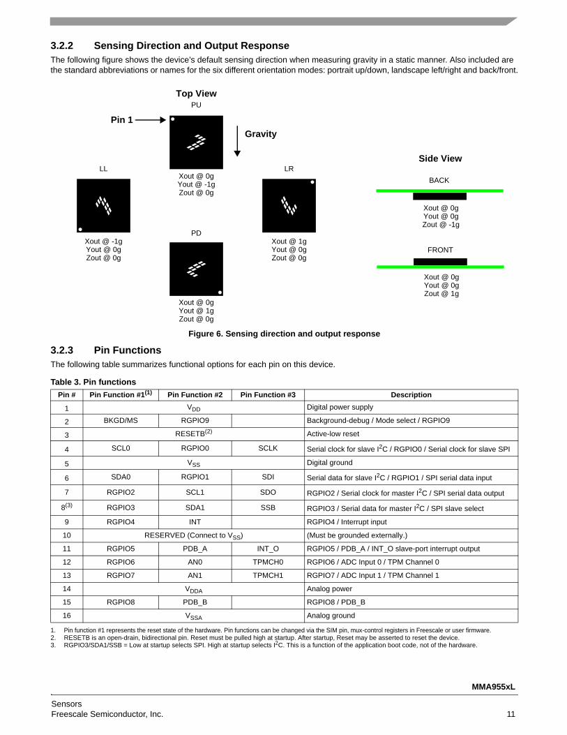
3.2.2 Sensing Direction and Output ResponseThe following figure shows the device’s default sensing direction when measuring gravity in a static manner. Also included are the standard abbreviations or names for the six different orientation modes: portrait up/down, landscape left/right and back/front.
Figure 6. Sensing direction and output response
3.2.3 Pin FunctionsThe following table summarizes functional options for each pin on this device.
Table 3. Pin functionsPin # Pin Function #1(1)
1. Pin function #1 represents the reset state of the hardware. Pin functions can be changed via the SIM pin, mux-control registers in Freescale or user firmware.
Pin Function #2 Pin Function #3 Description
1 VDD Digital power supply
2 BKGD/MS RGPIO9 Background-debug / Mode select / RGPIO9
3 RESETB(2)
2. RESETB is an open-drain, bidirectional pin. Reset must be pulled high at startup. After startup, Reset may be asserted to reset the device.
Active-low reset
4 SCL0 RGPIO0 SCLK Serial clock for slave I2C / RGPIO0 / Serial clock for slave SPI
5 VSS Digital ground
6 SDA0 RGPIO1 SDI Serial data for slave I2C / RGPIO1 / SPI serial data input
7 RGPIO2 SCL1 SDO RGPIO2 / Serial clock for master I2C / SPI serial data output
8(3)
3. RGPIO3/SDA1/SSB = Low at startup selects SPI. High at startup selects I2C. This is a function of the application boot code, not of the hardware.
RGPIO3 SDA1 SSB RGPIO3 / Serial data for master I2C / SPI slave select
9 RGPIO4 INT RGPIO4 / Interrupt input
10 RESERVED (Connect to VSS) (Must be grounded externally.)
11 RGPIO5 PDB_A INT_O RGPIO5 / PDB_A / INT_O slave-port interrupt output
12 RGPIO6 AN0 TPMCH0 RGPIO6 / ADC Input 0 / TPM Channel 0
13 RGPIO7 AN1 TPMCH1 RGPIO7 / ADC Input 1 / TPM Channel 1
14 VDDA Analog power
15 RGPIO8 PDB_B RGPIO8 / PDB_B
16 VSSA Analog ground
Top ViewPU
GravityPin 1
Xout @ 0gYout @ -1gZout @ 0g
Xout @ 1gYout @ 0gZout @ 0g
Xout @ 0gYout @ 1gZout @ 0g
Xout @ -1gYout @ 0gZout @ 0g
LL
PD
LRSide View
FRONT
Xout @ 0gYout @ 0gZout @ 1g
BACK
Xout @ 0gYout @ 0gZout @ -1g

MMA955xL
Sensors12 Freescale Semiconductor, Inc.
3.3 Pin Function DescriptionsThis section provides a brief description of the various pin functions available on the MMA955xL platform. Ten of the device pins are multiplexed with Rapid GPIO (RGPIO) functions. The “Pin Function #1” column in Table 3 on page 11 lists which function is active when the hardware exits the reset state. Freescale or user firmware can use the pin mux-control registers in the System Integration Module (SIM) to change pin assignments for each pin after reset. For detailed information about these registers, see the MMA955xL Three-Axis Accelerometer Reference Manual (MMA955xLRM).
VDD and VSS: Digital power and ground. VDD is nominally 1.8V.
VDDA and VSSA: Analog power and ground. VDDA is nominally 1.8V. To optimize performance, the VDDA line can be filtered to remove any digital noise that can be present on the 1.8V supply. (See Figure 5 and Figure 6 on page 17.)
RESETB: The RESETB pin is an open-drain, bidirectional pin with an internal, weak, pullup resistor. At start up, it is configured as an input pin, but also can be programmed to become bidirectional. Using this feature, the MMA955xL device can reset external devices for any purpose other than power-on reset. Reset must be pulled high at startup. After startup, Reset may be asserted to reset the device. The total external capacitance to ground has to be limited when using RESETB-pin, output-drive capability. For more details, see the “System Integration Module” chapter of the MMA955xL Three-Axis Accelerometer Reference Manual (MMA955xLRM).
Slave I2C port: SDA0 and SCL0: These are the slave-I2C data and clock signals, respectively. The MMA955xL device can be controlled via the serial port or via the slave SPI interface.
Master I2C: SDA1 and SCL1: These are the master-I2C clock and data signals, respectively.
Analog-to-Digital Conversion: AN0, AN1: The on-chip ADC can be used to perform a differential, analog-to-digital conversion based on the voltage present across pins AN0(-) and AN1(+). Conversions for these pins are at the same Output Data Rate (ODR) as the MEMS transducer signals. Input levels are limited to 1.8V differential.
Rapid General Purpose I/O: RGPIO[9:0]: The ColdFire V1 CPU has a feature called Rapid GPIO (RGPIO). This is a 16-bit, input/output port with single-cycle write, set, clear, and toggle functions available to the CPU. The MMA955xL device brings out the lower 10 bits of that port as pins of the device.
Interrupts: INT: This input pin can be used to wake the CPU from a deep-sleep mode. It can be programmed to trigger on either rising or falling edge, or high or low level. This pin operates as a Level-7 (high-priority) interrupt.
Debug/Mode Control: BKGD/MS: At start up, this pin operates as mode select. If this pin is pulled high during start up, the CPU will boot normally and run code. If this pin is pulled low during start up, the CPU will boot into active Background-Debug Mode (BDM). In BDM, this pin operates as a bidirectional, single-wire, background-debug port. It can be used by development tools for downloading code into on-chip RAM and flash and to debug that code.
Timer: PDB_A and PDB_B: These are the two outputs of the programmable delay block.
Slave SPI Interface: SCLK, SDI, SDO and SSB: These pins control the slave SPI clock, data in, data out, and slave-select signals, respectively. The MMA955xL platform can be controlled via this serial port or via the slave-I2C interface. SBB has a spe-cial function at startup that selects the Slave interface mode. Low at startup selects SPI and high selects I2C.
INT_O: The slave-port output interrupt pin. This pin can be used to flag the host when a response to a command is available to read on the slave port.
TPMCH0 and TPMCH1: The I/O pin associated with 16-bit, TPM channel 0 and 1.
3.4 System Connections3.4.1 Power SequencingAn internal circuit powered by VDDA provides the device with a power-on-reset signal. In order for this signal to be properly rec-ognized, it is important that VDD is powered up before or simultaneously with VDDA. The voltage potential between VDD and VDDA must not be allowed to exceed the value specified in Table 7 on page 17.
3.4.2 Layout Recommendations• Provide a low-impedance path from the board power supply to each power pin (VDD and VDDA) on the device and from the
board ground to each ground pin (VSS and VSSA).• Place 0.01 to 0.1-µF capacitors as close as possible to the package supply pins to meet he minimum bypass requirement.
The recommended bypass configuration is to place one bypass capacitor on each of the VDD/VSS pairs. VDDA/VSSA. ceramic and tantalum capacitors tend to provide better tolerances.
• Ensure that capacitor leads and associated printed-circuit traces that connect to the chip VDD and VSS (GND) pins are as short as possible.
• Bypass the power and ground with a capacitor of approximately 1 µF and a number of 0.1-µF ceramic capacitors.

MMA955xL
SensorsFreescale Semiconductor, Inc. 13
• Minimize PCB trace lengths for high-frequency signals. This is especially critical in systems with higher capacitive loads that could create higher transient currents in the VDD and VSS circuits.
• Take special care to minimize noise levels on the VDDA and VSSA pins.• Use separate power planes for VDD and VDDA and separate ground planes for VSS and VSSA. Connect the separate analog
and digital power and ground planes as close as possible to power supply outputs. If both analog circuit and digital circuits are powered by the same power supply, it is advisable to connect a small inductor or ferrite bead in series with both the VDDA and VSSA traces.
• Physically separate the analog components from noisy digital components by ground planes. Do not place an analog trace in parallel with digital traces. It is also desirable to place an analog ground trace around an analog signal trace to isolate it from digital traces.
• Provide an interface to the BKGD/MS pin if in-circuit debug capability is desired.• Ensure that resistors RP1 and RP2, in the following figure, match the requirements stated in the I2C standard. For the shown
configuration, the value of 4.7 kΩ would be appropriate.
3.4.3 MMA955xL Platform as an Intelligent SlaveI2C pullup resistors, a ferrite bead, and a few bypass capacitors are all that are required to attach this device to a host platform. The basic configurations are shown in the following two figures. In addition, the RGPIO pins can be programmed to generate interrupts to a host platform in response to the occurrence of real-time application events. In this case, the pins should be routed to the external interrupt pins of the CPU.
Figure 7. Platform as an I2C slave
Quiet VDDA forbest performance
1.8V
1.8V
1.8V
1.8V
1.8V
C41μF
C30.1μF
U1MMA955X
1
3
6
4
5
2
7 8
9
10
11
12
13
141516
VDD
RESETB
SD
A0/
IO1/
SD
ISCL0/IO0/SCLK
VSS
BKGD/MS/IO9
IO2/
SC
L1/S
DO
IO3/
SD
A1/
SB
B
IO4/INT
VSS
IO5/PDB_A/INT_O
IO6/AN0
IO7/AN1
VD
DA
IO8/
PD
B_B
VS
SA
R2
4.7KΩ
R3
4.7KΩ
L110μF BEAD
1 2
C11μF
C20.1μF
R1
4.7KΩ
R4
4.7KΩ
INT_OUT
I2C_CLK
I2C_DATA

MMA955xL
Sensors14 Freescale Semiconductor, Inc.
Figure 8. Platform as an SPI slave
Quiet VDDA forbest performance 1.8V
1.8V
1.8V
U1MMA955X
1
3
6
4
5
2
7 8
9
10
11
12
13
141516
VDD
RESETB
SD
A0/
IO1/
SD
ISCL0/IO0/SCLK
VSS
BKGD/MS/IO9
IO2/
SC
L1/S
DO
IO3/
SD
A1/
SB
B
IO4/INT
VSS
IO5/PDB_A/INT_O
IO6/AN0
IO7/AN1
VD
DA
IO8/
PD
B_B
VS
SA
C20.1μF
C11μF
L110μH BEAD
1 2
C41μF
C30.1μF
R1
4.7KΩ
R4
10KΩ
INT_OUT
SPI_CLK
SPI_DI (MOSI)
SPI_DO (MISO)
SPI_EN

MMA955xL
SensorsFreescale Semiconductor, Inc. 15
3.4.4 MMA955xL Platform as a Sensor HubThe MMA955xL device includes a powerful, 32-bit ColdFire V1 CPU; a second, I2C bus; and one, external analog input. These features can all be monitored using the on-chip ADC.
The combination of low power consumption and powerful features mean that the MMA955xL platform can effectively operate as a power controller for handheld units such as cell phones, PDAs, and games. The host platform can put itself to sleep with con-fidence that the MMA955xL device will issue a wake request should any external event require its attention.
The following figure illustrates the MMA955xL device being used in this configuration. Observe how all that is required is a few bypass capacitors, a ferrite bead, and some pullup resistors for the I2C buses.
Figure 9. Platform as sensor hub
Quiet VDDA forbest performance
I2C DigitalSensors
DifferentialAnalogSensor
1.8V
1.8V
1.8V
1.8V
1.8V
C41μF
R1
4.7KΩ
C11μF
U1MMA955X
1
3
6
4
5
27 8
9
10
11
12
13
141516VDD
RESETB
SD
A0/
IO1/
SD
ISCL0/IO0/SCLK
VSS
BKGD/MS/IO9IO
2/S
CL1
/SD
O
IO3/
SD
A1/
SB
B
IO4/INT
VSS
IO5/PDB_A/INT_O
IO6/AN0
IO7/AN1
VD
DA
IO8/
PD
B_B
VS
SA
L110μF BEAD
1 2
C30.1μF
R2
4.7KΩ
R3
4.7KΩ
C20.1μF
R3
4.7KΩ
R4
4.7KΩI2C_DATA
I2C_CLK
INT_OUT
I2C_CLK
I2C_DATA
INT_IN
RESETB

MMA955xL
Sensors16 Freescale Semiconductor, Inc.
4 Mechanical and Electrical SpecificationsThis section contains electrical specification tables and reference timing diagrams for the MMA955xL device, including detailed information on power considerations, DC/AC electrical characteristics, and AC timing specifications.
4.1 DefinitionsCross-axis sensitivity The proportionality constant that relates a variation of accelerometer output to cross acceleration. This
sensitivity varies with the direction of cross acceleration and is primarily due to misalignment.Full range The algebraic difference between the upper and lower values of the input range. Refer to the input/
output characteristics.Hardware compensated Sensor modules on this device include hardware-correction factors for gain and offset errors that are
calibrated during factory test using a least-squares fit of the raw sensor data.Linearity error The deviation of the sensor output from a least-squares linear fit of the input/output data.Nonlinearity The systematic deviation from the straight line that defines the nominal input/output relationship.Pin group the clustering of device pins into a number of logical pin groupings to simplify and standardize electrical
data sheet parameters. Pin groups are defined in Section 4.2, “Pin Groups”.Software compensated Freescale’s advanced non-linear calibration functions that—with the first-order hardware gain and off-
set calibration features—improve sensor performance.Warm-up time The time from the initial application of power for a sensor to reach its specified performance under the
documented operating conditions.
4.2 Pin GroupsThe following pin groups are used throughout the remainder of this section.
Group 1 RESETBGroup 2 RESERVEDGroup 3 RGPIO[9:0]
4.3 Absolute Maximum RatingsAbsolute maximum ratings are stress ratings only and operation at these maximums is not guaranteed. Stress beyond the limits specified can affect device reliability or cause permanent damage to the device. For functional operating conditions, refer to the remaining tables in this section.
This device contains circuitry to protect against damage due to high static voltage or electrical fields. It is advised, however, that normal precautions be taken to avoid application of any voltages higher than maximum-rated voltages to this high-impedance circuit. Reliability of operation is enhanced if unused inputs are tied to an appropriate logic voltage level (for instance, either VSS or VDD).
Table 4. Absolute maximum ratingsRating Symbol Minimum Maximum Unit
Digital supply voltage VDD -0.3 2.0 V
Analog supply voltage VDDA -0.3 2.0 V
Voltage difference, VDD to VDDA VDD - VDDA -0.1 0.1 V
Voltage difference, VSS to VSSA VSS - VSSA -0.1 0.1 V
Input voltage VIn -0.3 VDD + 0.3 V
Input/Output pin-clamp current IC -20 20 mA
Output voltage range (Open-Drain Mode) VOUTOD -0.3 VDD + 0.3 V
Storage temperature Tstg -40 125 °C
Mechanical shock SH 5k g

MMA955xL
SensorsFreescale Semiconductor, Inc. 17
4.4 Operating Conditions
4.5 Electrostatic Discharge (ESD) and Latch-up Protection Characteristics
4.6 General DC Characteristics
Table 5. Nominal operating conditionsRating Symbol Condition(s) Min Typ Max Unit
Digital supply voltage VDD 1.71 1.8 1.89 V
Analog supply voltage VDDA 1.71 1.8 1.89 V
Voltage difference, VDD to VDDA VDD - VDDA -0.1 0.1 V
Voltage difference, VSS to VSSA VSS - VSSA -0.1 0.1 V
Input voltage high VIH 0.7*VDD VDD+0.1 V
Input voltage low VIL VSS - 0.3 0.3*VDD V
Operating temperature TA -40 25 85 °C
Table 6. ESD and latch-up protection characteristics
Rating Symbol Min Max Unit
Human Body Model (HBM) VHBM ±2000 — V
Machine Model (MM) VMM ±200 — V
Charge Device Model (CDM) VCDM ±500 — V
Latch-up current at 85°C ILAT ±100 — mA
Table 7. DC characteristics(1)
1.All conditions at nominal supply: VDD = VDDA = 1.8V.
Characteristic Symbol Condition(s)(2)
2.Pin groups are defined in “Pin Groups” on page 16.
Min Typ Max Unit
Output voltage high• Low-drive strength• High-drive strength
VOH
Pin Groups 1 and 3ILOAD = -2 mAILOAD = -3 mA
VDD - 0.5 — — V
Output voltage low• Low-drive strength• High-drive strength
VOL
Pin Groups 1 and 3ILOAD = 2 mAILOAD = 3 mA
— — 0.5 V
Output-low currentMax total IOL for all ports
IOLT 24 mA
Output-high currentMax total IOH for all ports
IOHT 24 mA
Input-leakage current |IIN| Pin Group 2Vin = VDD or VSS
— 0.1 1 µA
Hi-Z (off-state) leakage current |IOZ|Pin Group 3 input resistors disabledVin = VDD or VSS
— 0.1 1 µA
Pullup resistor RPU when enabled 17.5 52.5 KΩ
Power-on-reset voltage VPOR 1.50 V
Power-on-reset hysteresis VPOR-hys 100 mV
Input-pin capacitance CIN 7 pF
Output-pin capacitance COUT 7 pF
MMA955xL
Sensors18 Freescale Semiconductor, Inc.
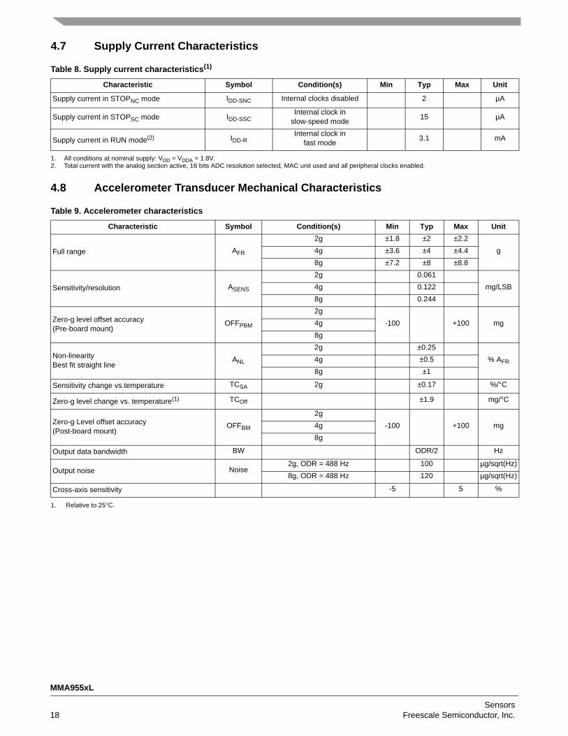
4.7 Supply Current Characteristics
4.8 Accelerometer Transducer Mechanical Characteristics
Table 8. Supply current characteristics(1)
1. All conditions at nominal supply: VDD = VDDA = 1.8V.
Characteristic Symbol Condition(s) Min Typ Max Unit
Supply current in STOPNC mode IDD-SNC Internal clocks disabled 2 µA
Supply current in STOPSC mode IDD-SSCInternal clock in
slow-speed mode 15 µA
Supply current in RUN mode(2)
2. Total current with the analog section active, 16 bits ADC resolution selected, MAC unit used and all peripheral clocks enabled.
IDD-RInternal clock in
fast mode 3.1 mA
Table 9. Accelerometer characteristics
Characteristic Symbol Condition(s) Min Typ Max Unit
Full range AFR
2g ±1.8 ±2 ±2.2g4g ±3.6 ±4 ±4.4
8g ±7.2 ±8 ±8.8
Sensitivity/resolution ASENS
2g 0.061mg/LSB4g 0.122
8g 0.244
Zero-g level offset accuracy (Pre-board mount)
OFFPBM
2g-100 +100 mg4g
8g
Non-linearityBest fit straight line
ANL
2g ±0.25% AFR4g ±0.5
8g ±1
Sensitivity change vs.temperature TCSA 2g ±0.17 %/°C
Zero-g level change vs. temperature(1)
1. Relative to 25°C.
TCOff ±1.9 mg/°C
Zero-g Level offset accuracy (Post-board mount)
OFFBM
2g-100 +100 mg4g
8g
Output data bandwidth BW ODR/2 Hz
Output noise Noise2g, ODR = 488 Hz 100 µg/sqrt(Hz)8g, ODR = 488 Hz 120 µg/sqrt(Hz)
Cross-axis sensitivity -5 5 %
MMA955xL
SensorsFreescale Semiconductor, Inc. 19
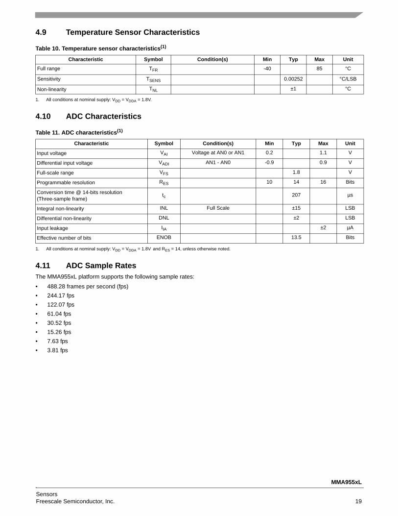
4.9 Temperature Sensor Characteristics
4.10 ADC Characteristics
4.11 ADC Sample RatesThe MMA955xL platform supports the following sample rates:
• 488.28 frames per second (fps)• 244.17 fps• 122.07 fps• 61.04 fps• 30.52 fps• 15.26 fps• 7.63 fps• 3.81 fps
Table 10. Temperature sensor characteristics(1)
1. All conditions at nominal supply: VDD = VDDA = 1.8V.
Characteristic Symbol Condition(s) Min Typ Max Unit
Full range TFR -40 85 °C
Sensitivity TSENS 0.00252 °C/LSB
Non-linearity TNL ±1 °C
Table 11. ADC characteristics(1)
1. All conditions at nominal supply: VDD = VDDA = 1.8V and RES = 14, unless otherwise noted.
Characteristic Symbol Condition(s) Min Typ Max Unit
Input voltage VAI Voltage at AN0 or AN1 0.2 1.1 V
Differential input voltage VADI AN1 - AN0 -0.9 0.9 V
Full-scale range VFS 1.8 V
Programmable resolution RES 10 14 16 Bits
Conversion time @ 14-bits resolution(Three-sample frame)
tc 207 µs
Integral non-linearity INL Full Scale ±15 LSB
Differential non-linearity DNL ±2 LSB
Input leakage IIA ±2 µA
Effective number of bits ENOB 13.5 Bits

MMA955xL
Sensors20 Freescale Semiconductor, Inc.
4.12 AC Electrical CharacteristicsTests are conducted using the input levels specified in Table 5 on page 17. Unless otherwise specified, propagation delays are measured from the 50-percent to 50-percent point. Rise and fall times are measured between the 10-percent and 90-percent points, as shown in the following figure.
Figure 10. Input signal measurement referencesThe subsequent figure shows the definitions of the following signal states:
• Active state, when a bus or signal is driven and enters a low-impedance state• Three-stated, when a bus or signal is placed in a high-impedance state• Data Valid state, when a signal level has reached VOL or VOH• Data Invalid state, when a signal level is in transition between VOL and VOH
Figure 11. Signal states
4.13 General Timing Control
Table 12. General timing characteristics(1)
1. All conditions at nominal supply: VDD = VDDA = 1.8 V
Characteristic Symbol Condition(s) Min Typ Max UnitVDD rise time Trvdd 10% to 90% 1 ms
POR release delay(2)
2. This is the time measured from VDD = VPOR until the internal reset signal is released.
TPOR Power-up 0.35 1.5 ms
Warm-up time TWU From STOPNC 7 sample periods
Frequency of operationFOPH Full Speed Clock 8 MHzFOPL Slow Clock 62.5 KHz
System clock periodtCYCH Full Speed Clock 125 nstCYCL Slow Clock 16 μs
Full/Slow clock ratio 128
Oscillator frequency absolute accuracy @ 25°C Full Speed Clock -5 +5 %
Oscillator frequency variation over temperature(-40°C to 85°C vs. ambient)
Slow Clock -6 +6 %
Minimum RESET assertion duration tRA 4T(3)
3. In the formulas, T = 1 system clock cycle. In full speed mode, T is nominally 125 ns. In slow speed mode, T is nominally 16 μs.
VIH
VILFall Time
Input Signal
Note: The midpoint is VIL + (VIH – VIL)/2.
Midpoint1
Low High90%50%10%
Rise Time
Data Invalid State
Data1
Data3-stated
Data3 Valid
Data2 Data3
Data1 Valid
Data Active Data Active
Data1 Valid
MMA955xL
SensorsFreescale Semiconductor, Inc. 21
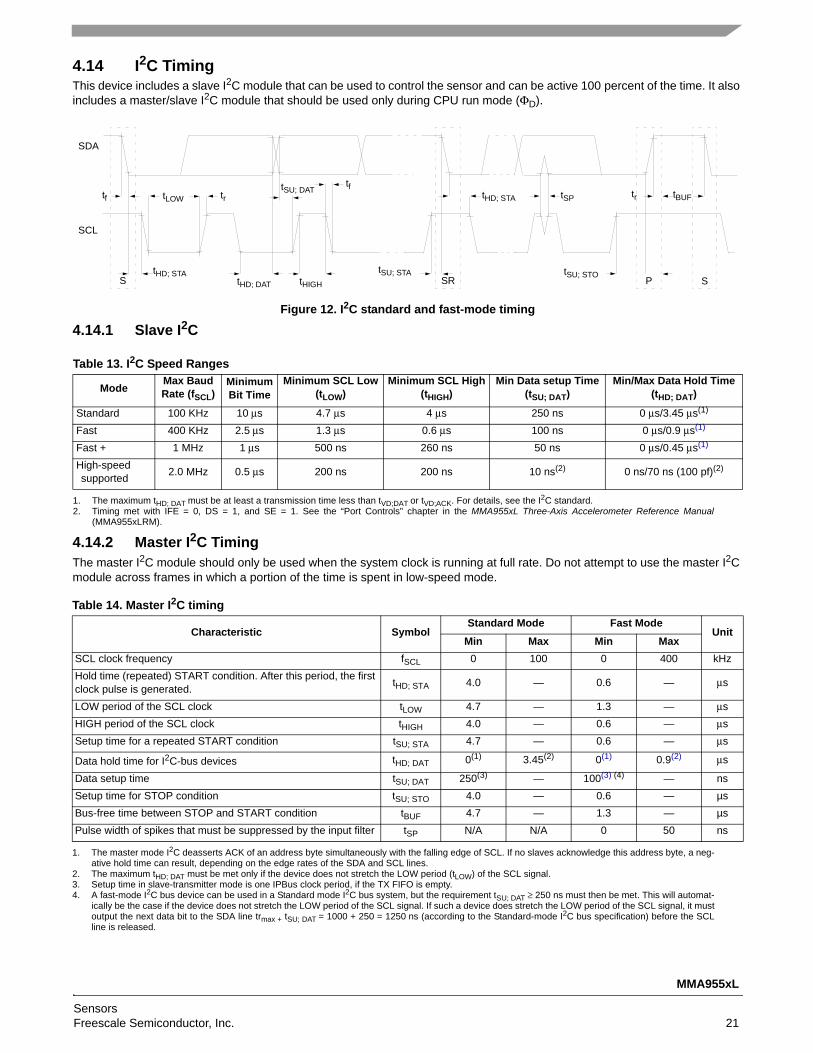
4.14 I2C TimingThis device includes a slave I2C module that can be used to control the sensor and can be active 100 percent of the time. It also includes a master/slave I2C module that should be used only during CPU run mode (ΦD).
Figure 12. I2C standard and fast-mode timing
4.14.1 Slave I2C
4.14.2 Master I2C TimingThe master I2C module should only be used when the system clock is running at full rate. Do not attempt to use the master I2C module across frames in which a portion of the time is spent in low-speed mode.
Table 13. I2C Speed Ranges
ModeMax BaudRate (fSCL)
MinimumBit Time
Minimum SCL Low(tLOW)
Minimum SCL High(tHIGH)
Min Data setup Time(tSU; DAT)
Min/Max Data Hold Time(tHD; DAT)
Standard 100 KHz 10 μs 4.7 μs 4 μs 250 ns 0 μs/3.45 μs(1)
1. The maximum tHD; DAT must be at least a transmission time less than tVD;DAT or tVD;ACK. For details, see the I2C standard.
Fast 400 KHz 2.5 μs 1.3 μs 0.6 μs 100 ns 0 μs/0.9 μs(1)
Fast + 1 MHz 1 μs 500 ns 260 ns 50 ns 0 μs/0.45 μs(1)
High-speedsupported 2.0 MHz 0.5 μs 200 ns 200 ns 10 ns(2) 0 ns/70 ns (100 pf)(2)
2. Timing met with IFE = 0, DS = 1, and SE = 1. See the “Port Controls” chapter in the MMA955xL Three-Axis Accelerometer Reference Manual(MMA955xLRM).
Table 14. Master I2C timing
Characteristic SymbolStandard Mode Fast Mode
UnitMin Max Min Max
SCL clock frequency fSCL 0 100 0 400 kHzHold time (repeated) START condition. After this period, the first clock pulse is generated. tHD; STA 4.0 — 0.6 — μs
LOW period of the SCL clock tLOW 4.7 — 1.3 — μsHIGH period of the SCL clock tHIGH 4.0 — 0.6 — μsSetup time for a repeated START condition tSU; STA 4.7 — 0.6 — μs
Data hold time for I2C-bus devices tHD; DAT 0(1)
1. The master mode I2C deasserts ACK of an address byte simultaneously with the falling edge of SCL. If no slaves acknowledge this address byte, a neg-ative hold time can result, depending on the edge rates of the SDA and SCL lines.
3.45(2)
2. The maximum tHD; DAT must be met only if the device does not stretch the LOW period (tLOW) of the SCL signal.
0(1) 0.9(2) μs
Data setup time tSU; DAT 250(3)
3. Setup time in slave-transmitter mode is one IPBus clock period, if the TX FIFO is empty.
— 100(3) (4)
4. A fast-mode I2C bus device can be used in a Standard mode I2C bus system, but the requirement tSU; DAT ≥ 250 ns must then be met. This will automat-ically be the case if the device does not stretch the LOW period of the SCL signal. If such a device does stretch the LOW period of the SCL signal, it mustoutput the next data bit to the SDA line trmax + tSU; DAT = 1000 + 250 = 1250 ns (according to the Standard-mode I2C bus specification) before the SCLline is released.
— nsSetup time for STOP condition tSU; STO 4.0 — 0.6 — µsBus-free time between STOP and START condition tBUF 4.7 — 1.3 — µsPulse width of spikes that must be suppressed by the input filter tSP N/A N/A 0 50 ns
SDA
SCL
tHD; STAtHD; DAT
tLOWtSU; DAT
tHIGH
tSU; STASR P SS
tHD; STA tSP
tSU; STO
tBUFtf trtf
tr

MMA955xL
Sensors22 Freescale Semiconductor, Inc.
4.15 Slave SPI TimingThe following table describes the timing requirements for the SPI system. The “#” column refers to the numbered time period in Figure 13.
Figure 13. SPI slave timing
Table 15. Slave SPI timing
# Function Symbol Min Max Unit
— Operating frequency fop 0 FOPH/4 Hz
1 SCLK period tSCLK 4 — tCYCH
2 Enable lead time tLead 0.5 — tCYCH
3 Enable lag time tLag 0.5 — tCYCH
4 Clock (SCLK) high or low time tWSCLK 200 — ns
5 Data setup time (inputs) tSU 15 — ns
6 Data-hold time (inputs) tHI 25 — ns
7 Access time ta — 25 ns
8 SDO-disable time tdis — 25 ns
9 Data valid (after SCLK edge) tv — 25 ns
10 Data-hold time (outputs) tHO 0 — ns
11Rise time
InputOutput
tRItRO
——
2525
nsns
12Fall time
InputOutput
tFItFO
——
2525
nsns
SCLK(INPUT)
SDI(INPUT)
SDO(OUTPUT)
SS(INPUT)
MSB IN
BIT 6 . . . 1
LSB IN
MSB OUT SLAVE LSB OUT
BIT 6 . . . 1
NOTE:
SLAVE SEENOTE
1. Not defined but normally MSB of character just received.
121
<
11 3
42 4
7
5 6
9
8
1010
MMA955xL
SensorsFreescale Semiconductor, Inc. 23
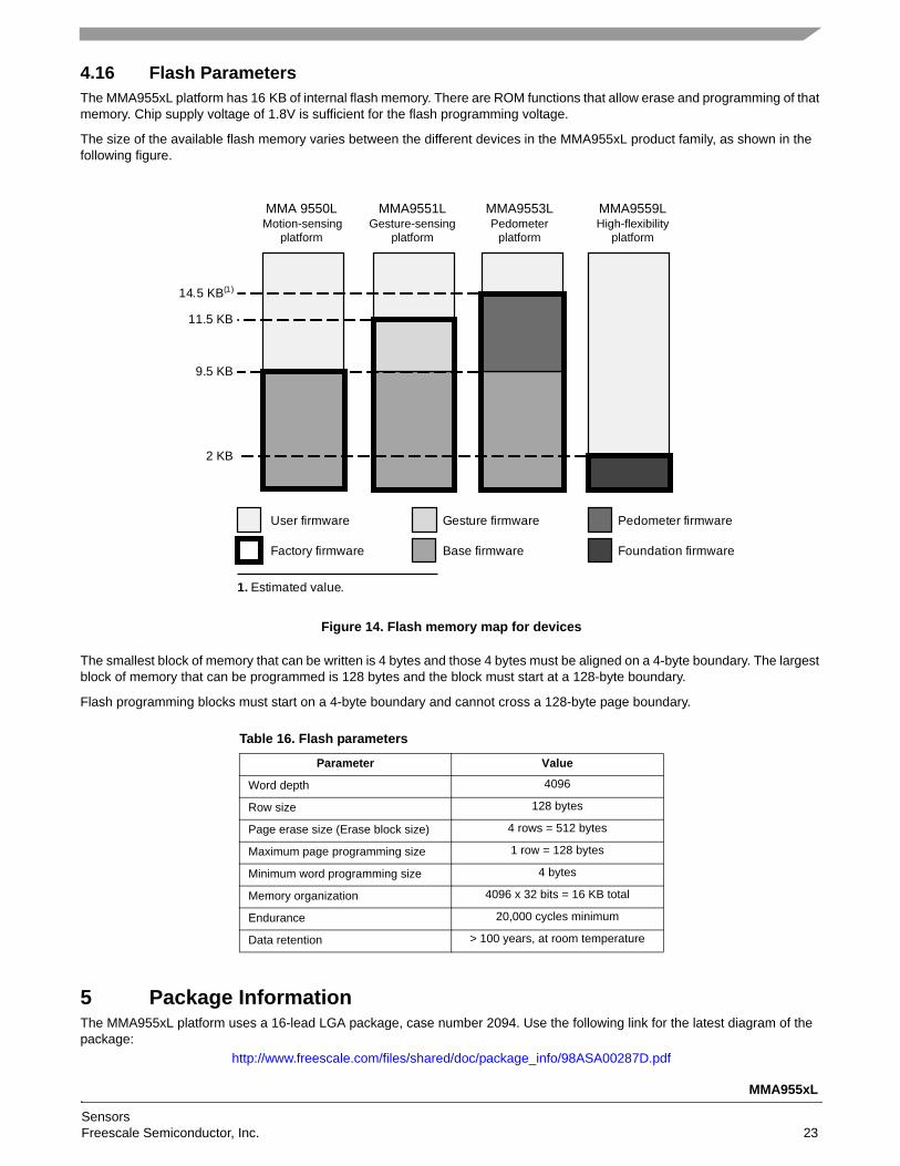
4.16 Flash ParametersThe MMA955xL platform has 16 KB of internal flash memory. There are ROM functions that allow erase and programming of that memory. Chip supply voltage of 1.8V is sufficient for the flash programming voltage.
The size of the available flash memory varies between the different devices in the MMA955xL product family, as shown in the following figure.
The smallest block of memory that can be written is 4 bytes and those 4 bytes must be aligned on a 4-byte boundary. The largest block of memory that can be programmed is 128 bytes and the block must start at a 128-byte boundary.
Flash programming blocks must start on a 4-byte boundary and cannot cross a 128-byte page boundary.
5 Package InformationThe MMA955xL platform uses a 16-lead LGA package, case number 2094. Use the following link for the latest diagram of the package:
http://www.freescale.com/files/shared/doc/package_info/98ASA00287D.pdf
Figure 14. Flash memory map for devices
Table 16. Flash parameters
Parameter Value
Word depth 4096
Row size 128 bytes
Page erase size (Erase block size) 4 rows = 512 bytes
Maximum page programming size 1 row = 128 bytes
Minimum word programming size 4 bytes
Memory organization 4096 x 32 bits = 16 KB total
Endurance 20,000 cycles minimum
Data retention > 100 years, at room temperature
9.5 KB
User firmware Gesture firmware Pedometer firmware
Factory firmware Base firmware Foundation firmware
11.5 KB
14.5 KB(1)
2 KB
1. Estimated value.
MMA 9550L MMA9551L MMA9553L MMA9559LMotion-sensing Gesture-sensing Pedometer High-flexibility
platform platform platform platform

MMA955xL
Sensors24 Freescale Semiconductor, Inc.
6 Revision History
Revision number
Revision date
Description of changes
0 06/2011 Initial release of document.
1 10/2011 • Removed MMA9552L device from product family and added the MMA9559L device.• Added a features table and a package land diagram figure.• Modified block diagram• Inserted flash memory map figure

How to Reach Us:
Home Page:www.freescale.com
Web Support:http://www.freescale.com/support
USA/Europe or Locations Not Listed:Freescale Semiconductor, Inc.Technical Information Center, EL5162100 East Elliot RoadTempe, Arizona 852841-800-521-6274 or +1-480-768-2130www.freescale.com/support
Europe, Middle East, and Africa:Freescale Halbleiter Deutschland GmbHTechnical Information CenterSchatzbogen 781829 Muenchen, Germany+44 1296 380 456 (English)+46 8 52200080 (English)+49 89 92103 559 (German)+33 1 69 35 48 48 (French)www.freescale.com/support
Japan:Freescale Semiconductor Japan Ltd.HeadquartersARCO Tower 15F1-8-1, Shimo-Meguro, Meguro-ku,Tokyo 153-0064Japan0120 191014 or +81 3 5437 [email protected]
Asia/Pacific:Freescale Semiconductor China Ltd.Exchange Building 23FNo. 118 Jianguo RoadChaoyang DistrictBeijing 100022 China +86 010 5879 [email protected]
For Literature Requests Only:Freescale Semiconductor Literature Distribution Center1-800-441-2447 or +1-303-675-2140Fax: [email protected]
MMA955xLRev. 110/2011
RoHS-compliant and/or Pb-free versions of Freescale products have the functionality and electrical characteristics of their non-RoHS-compliant and/or non-Pb-free counterparts. For furtherinformation, see http:/www.freescale.com or contact your Freescale sales representative.
For information on Freescale’s Environmental Products program, go to http://www.freescale.com/epp.
Information in this document is provided solely to enable system and software implementers to use Freescale Semiconductor products. There are no express or implied copyright licenses granted hereunder to design or fabricate any integrated circuits or integrated circuits based on the information in this document.
Freescale Semiconductor reserves the right to make changes without further notice to any products herein. Freescale Semiconductor makes no warranty, representation or guarantee regarding the suitability of its products for any particular purpose, nor does Freescale Semiconductor assume any liability arising out of the application or use of any product or circuit, and specifically disclaims any and all liability, including without limitation consequential or incidental damages. “Typical” parameters that may be provided in Freescale Semiconductor data sheets and/or specifications can and do vary in different applications and actual performance may vary over time. All operating parameters, including “Typicals”, must be validated for each customer application by customer’s technical experts. Freescale Semiconductor does not convey any license under its patent rights nor the rights of others. Freescale Semiconductor products are not designed, intended, or authorized for use as components in systems intended for surgical implant into the body, or other applications intended to support or sustain life, or for any other application in which the failure of the Freescale Semiconductor product could create a situation where personal injury or death may occur. Should Buyer purchase or use Freescale Semiconductor products for any such unintended or unauthorized application, Buyer shall indemnify and hold Freescale Semiconductor and its officers, employees, subsidiaries, affiliates, and distributors harmless against all claims, costs, damages, and expenses, and reasonable attorney fees arising out of, directly or indirectly, any claim of personal injury or death associated with such unintended or unauthorized use, even if such claim alleges that Freescale Semiconductor was negligent regarding the design or manufacture of the part.
Freescale, the Freescale logo, and the Energy Efficient Solutions logo are trademarks of Freescale Semiconductor, Inc., Reg. U.S. Pat. & Tm. Off. Xtrinsic is a trademark of Freescale Semiconductor, Inc.
All other product or service names are the property of their respective owners.
© 2011 Freescale Semiconductor, Inc. All rights reserved.