Embed Size (px)
Citation preview

Mark Ermolov
Maxim Goryachy
Intel VISA: Through the Rabbit Hole

Disclaimer
The methods described here are risky and may damage or destroy your computer. We take no responsibility for any attempts inspired by our work
and do not guarantee the operability of anything.
2

Warning
1. All information provided here is a result of public software, firmware, and hardware analysis. This research may contain true mistakes and
inaccuracies.
2. Our access to Intel VISA is made possible by the Intel-SA-00086vulnerability that we detected, but you can try other methods. ;)
3. If you find mistakes, please let us know (email or Twitter).
3

Deep Intel CPU (Our View)
VT-xAVX
SSE
SGX
MSR Regs
TSX VT-d
SMM
MP HT
DCI
BootGuard
Microcode
ME
X86 Instruction set
QPI
TXT TraceHub
UNCORE
PMC
ISH
CAR
Probe Mode
Public Documentation
Partial Documentation
Private Documentation
DMI
UPI
4
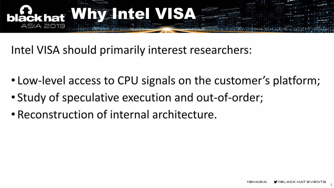
Why Intel VISA
Intel VISA should primarily interest researchers:
• Low-level access to CPU signals on the customer’s platform;
• Study of speculative execution and out-of-order;
•Reconstruction of internal architecture.
5
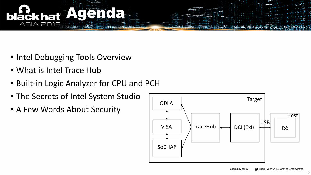
Agenda
• Intel Debugging Tools Overview
• What is Intel Trace Hub
• Built-in Logic Analyzer for CPU and PCH
• The Secrets of Intel System Studio
• A Few Words About Security
6
VISA
SoCHAP
TraceHub DCI (ExI)
Target
Host
ISSUSB
ODLA

Intel Debugging Tools Overview
VISA
SoCHAP
TraceHub DCI (ExI)
Target
Host
ISSUSB
ODLA
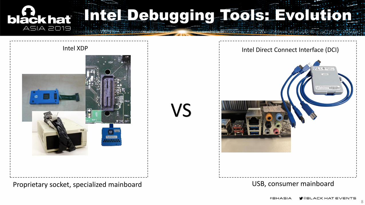
Intel Debugging Tools: Evolution
VS
Proprietary socket, specialized mainboard USB, consumer mainboard
Intel Direct Connect Interface (DCI)
8
Intel XDP

Intel DCI
• Intel DFx Abstraction Layout
• Check PCH GPIO pins
• Check DDR memory
• Check USB devices
• Check Direct Media Interface (DMI)
• Check CPU high precision event timer
• Check PCH PCIe bus/drivers
• Check PCH SMBus /devices
• ....
9

Intel Trace Hub
VISA
SoCHAP
TraceHub DCI (ExI)
Target
Host
ISSUSB
ODLA

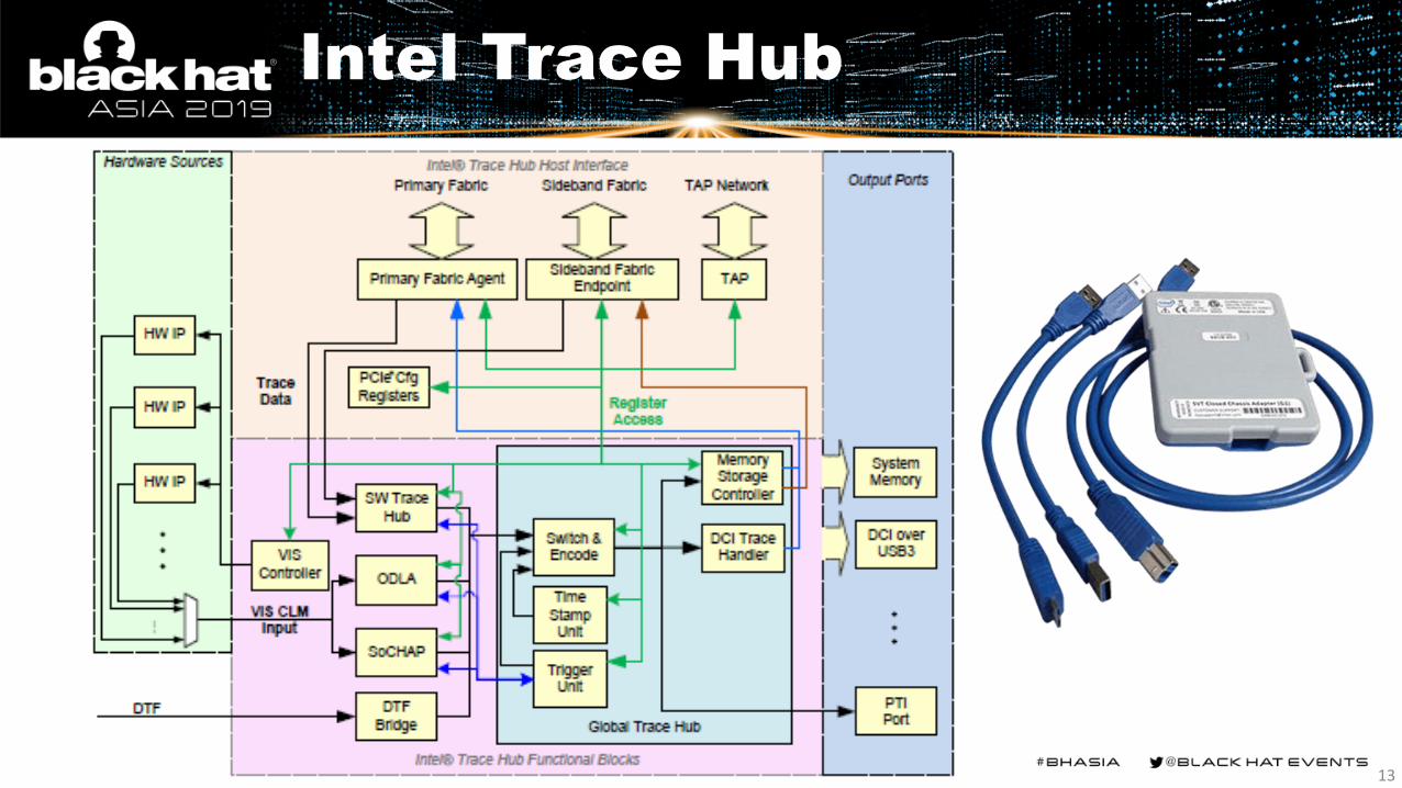
Intel PCH/SoC Hardware Tracing
• Integrated into Trace Hub.
• Consists of Intel VISA, ODLA, SoCHAP.
• Controlled by the Trace Hub MMIO CSR range.
• Uses Trace Hub components for trace data collection.
• Uses Common Trigger Sequencer for triggering capabilities.
• Supports all Trace Hub transports (DCI BSSB, DbC, HTI, and PTI via GPIO).
11
• A new Intel approach to collection of all trace data in a platform (since Skylake).
• The internal code name is North Peak (NPK).
• Supports software, firmware, and hardware tracing.
• Dedicated IP unit accessible by PCI, IOSF Side Band, JTAG.
• Consists of Trace Sources (Masters) and Global Trace Hub.
• Encodes trace data into the MIPI STPv2 protocol.
• Collects data into RAM, sends it to HW interfaces.
• Supports Intel Processor Trace and Architectural Events Tracing.
• Has Common Trigger Sequencer (CTS) for flexible control of trace masters.
Intel Trace Hub
12
Intel Trace Hub
13
Intel Trace Hub Software
• Software stack of two libraries: Trace Hub API and Trace Decode Engine.
• Each library is provided with native tools: npk_cfg64.exe and tde_boot.exe.
• Both libraries are configured by XMLs: npk.xml, visa.xml, tde.xml.
• Trace Hub API uses special Interview XML for HW events description.
• Trace Hub API serializes its state to *.tracecfg JSON.
• The software is installed as part of the Intel System Trace tool.
• There isn't any public (non-NDA) info about the libraries.
• The Linux version of the libraries has unstripped (function names) binaries.
14

Demo
CSME Tracing
15

Intel Visualization of Internal Signals Architecture (VISA*)
* From US 2017/0176523 A1, INTERFACES FOR WIRELESS DEBUGGING
VISA
SoCHAP
TraceHub DCI (ExI)
Target
Host
ISSUSB
ODLA

Intel VISA
• Stands for Visualization of Internal Signals Architecture.
• A network of hundreds of multiplexers routing debug signals to ODLA.
• Each IP unit selects a set of signals to be routed to VISA.
• Dedicated VISA Registers Controller (VRC) managing the network.
• Three types of multiplexers: CLM, PLM, and ULM.
• VISA uses native internal clocks.
• VISA can route IP signals and native clocks to external Logic Analyzer.
• Each multiplexer supports an advanced pattern generator.
17
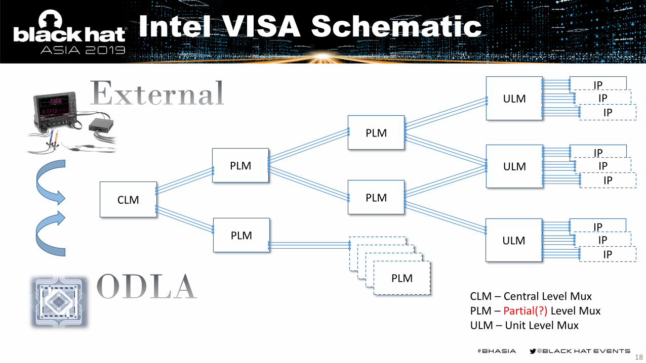
Intel VISA Schematic
CLM
ULM
PLM
IPIPIP
ULMIPIPIP
ULMIPIPIP
PLM
PLMPLM
PLMPLM
PLM
PLM
CLM – Central Level MuxPLM – Partial(?) Level MuxULM – Unit Level Mux
18

Intel VISA Registers Controller (VRC)
• VRC defines fixed MMIO ranges for each Mux register.
• Each Mux has one control register for every output lane.
• VRC defines selectors for native clocks and for IP units signal groups.
• ULM lanes transmit one native clock and a group of IP signals.
• CLM and PLM lanes transmit lanes of other PLMs and ULMs.
• CLM and some ULMs have special xbar lanes for CTS and SoCHAP.
• VRC controls access to lane control registers.
• VRC has Replay RAM for automatic Intel VISA reconfiguration.
19
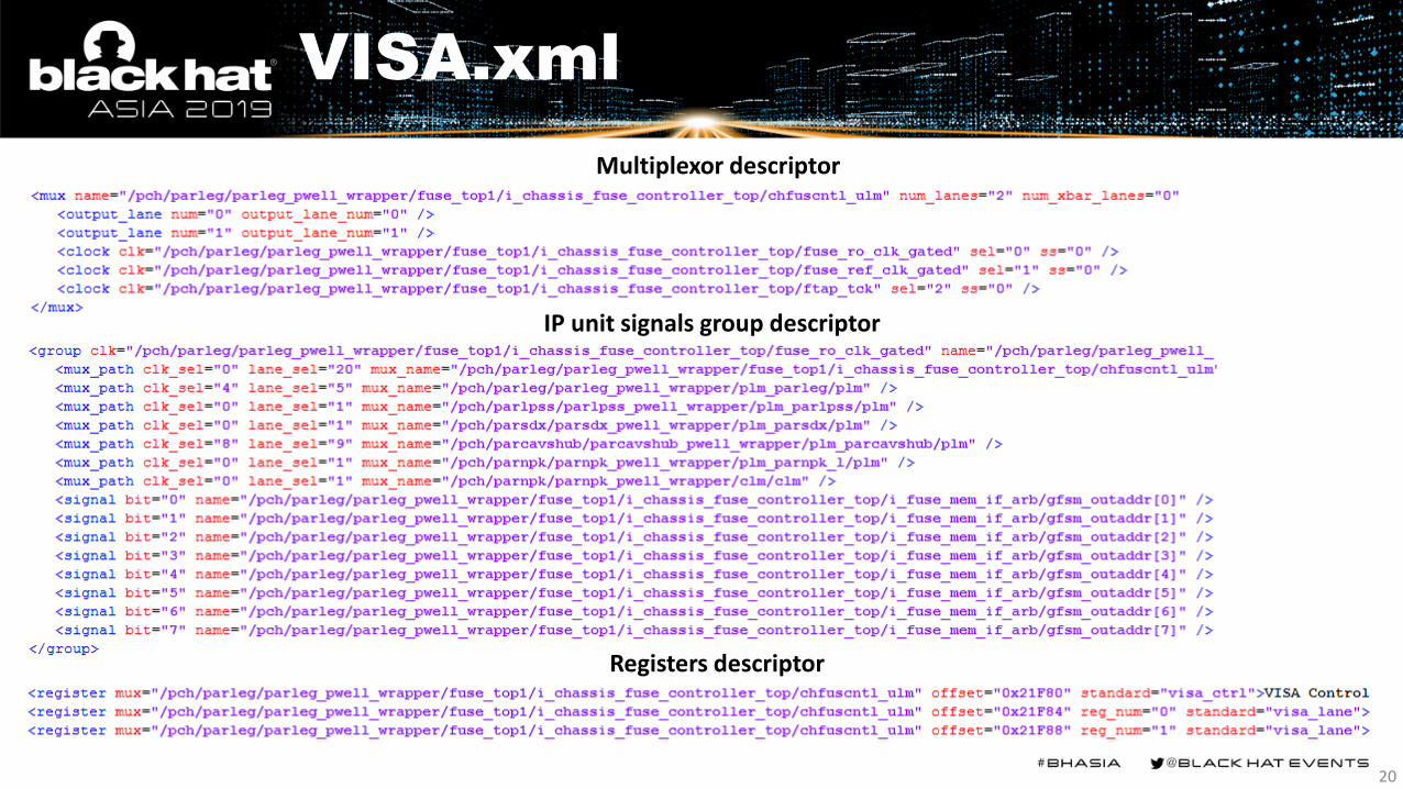
VISA.xml
Multiplexor descriptor
IP unit signals group descriptor
Registers descriptor
20

Our collection (Intel VISA XMLs)
Name SizeE:\visa\Trace\2019\0.050\win\targets\CNP\WHL\D0\green\config\npk\visa.xml 82610604E:\visa\Trace\2019\0.050\win\targets\CNP\CFL-S\B1\green\config\npk\visa.xml 82610604E:\visa\Trace\2019\0.033\win\targets\CNP\WHL\D0\green\config\npk\visa.xml 82610604E:\visa\Trace\2019\0.033\win\targets\CNP\CFL-S\B1\green\config\npk\visa.xml 82610604E:\visa\Trace\2019\0.014\win\targets\CNP\CFL-S\B1\green\config\npk\visa.xml 82610604E:\visa\Trace\2018\0.051\targets\BXT\P\D0\all\config\npk\visa.xml 43068808E:\visa\Trace\2018\0.051\targets\BXT\P\B0\all\config\npk\visa.xml 43068808E:\visa\Trace\2018\0.040\win\targets\BXT\P\D0\all\config\npk\visa.xml 43068808E:\visa\Trace\2018\0.040\win\targets\BXT\P\B0\all\config\npk\visa.xml 43068808E:\visa\Trace\2018\0.040\lin\targets\BXT\P\D0\all\config\npk\visa.xml 43068808E:\visa\Trace\2018\0.040\lin\targets\BXT\P\B0\all\config\npk\visa.xml 43068808E:\visa\Trace\2018\0.051\targets\LBG\SKX\B1\green\config\npk\visa.xml 35177433E:\visa\Trace\2018\0.051\targets\LBG\SKX\B0\green\config\npk\visa.xml 35177433E:\visa\Trace\2018\0.040\win\targets\LBG\SKX\B1\green\config\npk\visa.xml 35177433E:\visa\Trace\2018\0.040\win\targets\LBG\SKX\B0\green\config\npk\visa.xml 35177433E:\visa\Trace\2018\0.028\targets\LBG\SKX\B1\green\config\npk\visa.xml 35177433E:\visa\Trace\2018\0.028\targets\LBG\SKX\B0\green\config\npk\visa.xml 35177433E:\visa\Trace\2018\0.051\targets\LBG\SKX\A0\green\config\npk\visa.xml 35050304E:\visa\Trace\2018\0.040\win\targets\LBG\SKX\A0\green\config\npk\visa.xml 35050304E:\visa\Trace\2018\0.028\targets\LBG\SKX\A0\green\config\npk\visa.xml 35050304E:\visa\Trace\2018\0.051\targets\LBG\SKX\S0\green\config\npk\visa.xml 32140480E:\visa\Trace\2018\0.040\win\targets\LBG\SKX\S0\green\config\npk\visa.xml 32140480E:\visa\Trace\2018\0.028\targets\LBG\SKX\S0\green\config\npk\visa.xml 32140480E:\visa\Trace\2018\0.051\targets\KBP\X\H0\green\config\npk\visa.xml 21603327E:\visa\Trace\2018\0.051\targets\KBP\W\M0\green\config\npk\visa.xml 21603327E:\visa\Trace\2018\0.051\targets\KBP\H\A0\green\config\npk\visa.xml 21603327
21
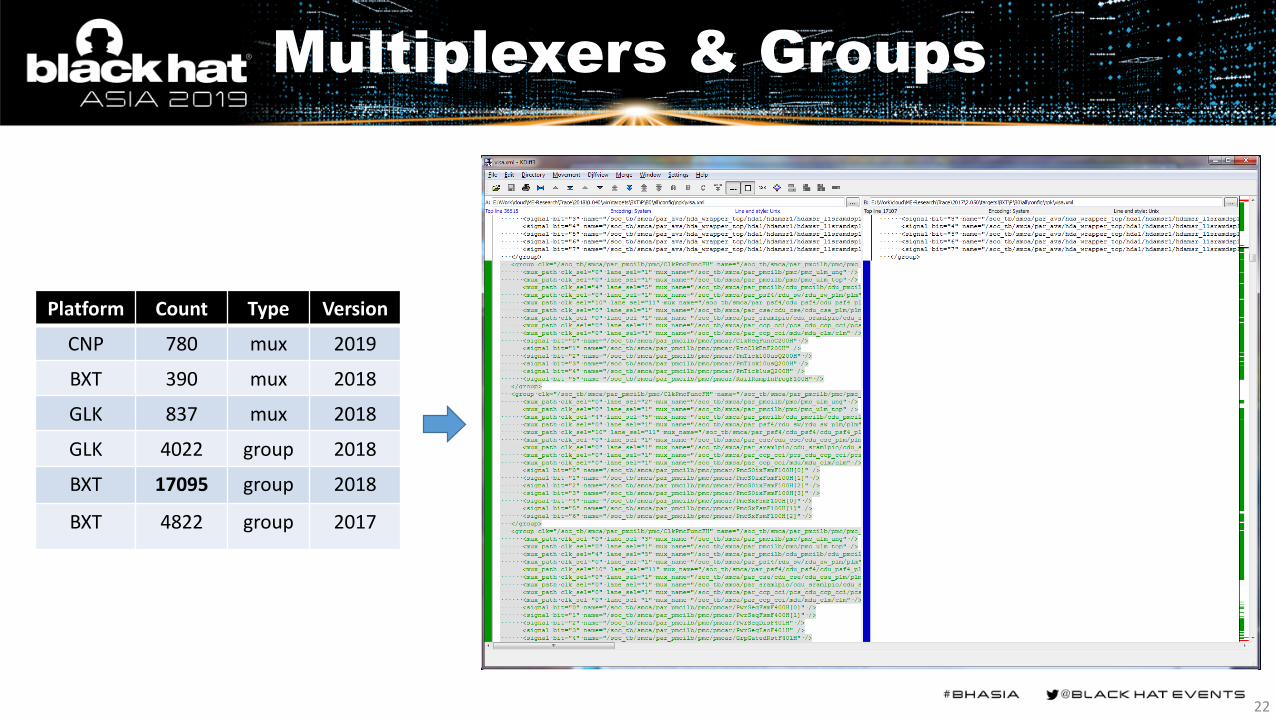
Multiplexers & Groups
Platform Count Type Version
CNP 780 mux 2019
BXT 390 mux 2018
GLK 837 mux 2018
GLK 4022 group 2018
BXT 17095 group 2018
BXT 4822 group 2017
22
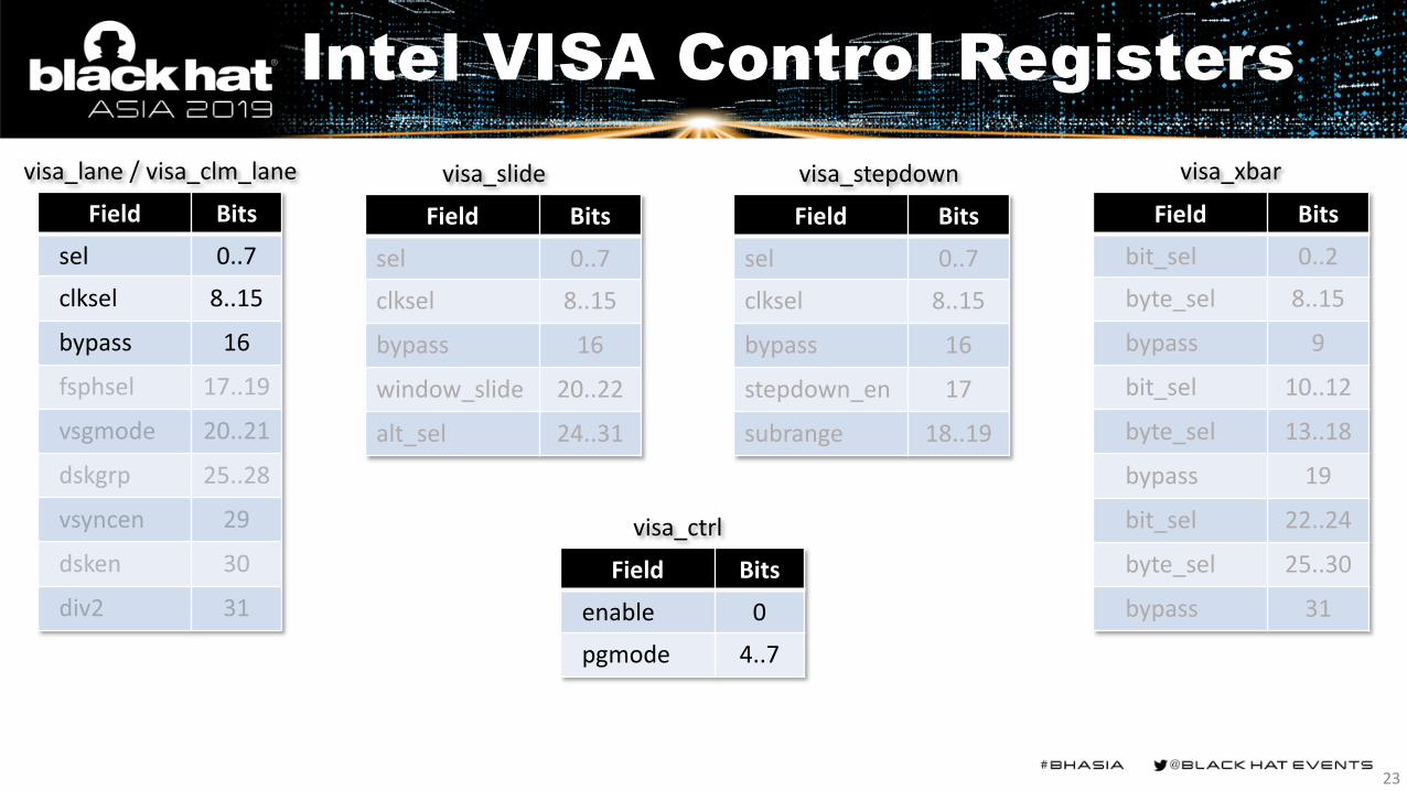
Intel VISA Control Registers
Field Bits
enable 0
pgmode 4..7
visa_ctrl
Field Bits
sel 0..7
clksel 8..15
bypass 16
visa_lane / visa_clm_lane
Field Bits
sel 0..7
clksel 8..15
bypass 16
window_slide 20..22
alt_sel 24..31
visa_slide
Field Bits
sel 0..7
clksel 8..15
bypass 16
stepdown_en 17
subrange 18..19
visa_stepdown
Field Bits
bit_sel 0..2
byte_sel 8..15
bypass 9
bit_sel 10..12
byte_sel 13..18
bypass 19
bit_sel 22..24
byte_sel 25..30
bypass 31
visa_xbar
23

Intel VISA Multiplexer
lane0
lane1
lane2
lane3
group0
group3
group2
group1
clock0
clock1
clock2
for each output lane:
clock sel
input lane/group sel
lane0
lane1
lane2
lane3
24

Intel On-Die Logic Analyzer (ODLA)
VISA
SoCHAP
TraceHub DCI (ExI)
Target
Host
ISSUSB
ODLA
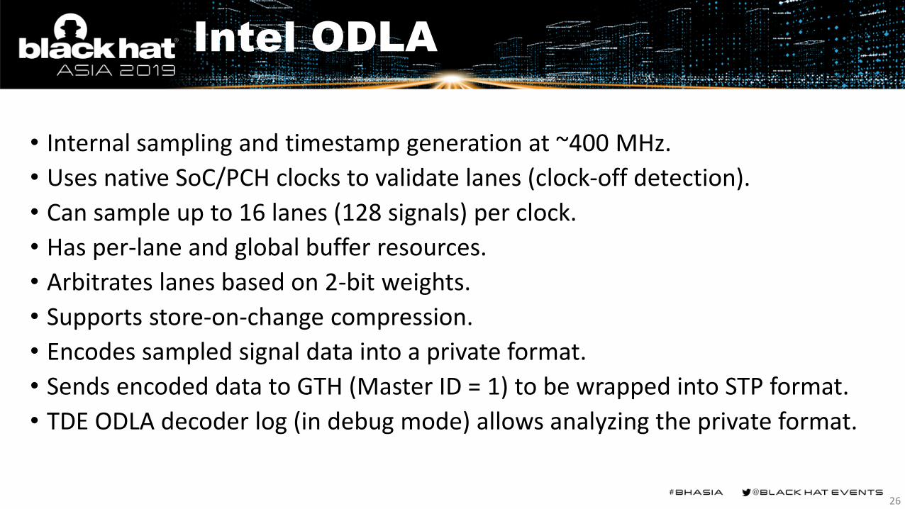
Intel ODLA
• Internal sampling and timestamp generation at ~400 MHz.
• Uses native SoC/PCH clocks to validate lanes (clock-off detection).
• Can sample up to 16 lanes (128 signals) per clock.
• Has per-lane and global buffer resources.
• Arbitrates lanes based on 2-bit weights.
• Supports store-on-change compression.
• Encodes sampled signal data into a private format.
• Sends encoded data to GTH (Master ID = 1) to be wrapped into STP format.
• TDE ODLA decoder log (in debug mode) allows analyzing the private format.
26

TDE ODLA Output Example
• Default file name – capture_vcd_decoder.vcd.• Placed at the path of the tde_boot64.exe session XML.• Contains a timestamp in ps for each sample interval.• Displays a special 1-bit lane A – trigger.• Lanes data are only in binary format.• Marks special conditions with the symbols u, w, -, x, z.
27

ODLA Packets Log
Time stamp injection Lanes data
Clock-off example
28

ODLA Tracing: Step by Step
Ensure that you have npk.xml and visa.xml for your platform.Check the following path:<Program Files>\IntelSWTools\system_debugger_[version]\system_trace\targets\[your platform]\[stepping]\[green|all]\config\npk
Create interview.xml describing the desired hardware events.See the next slide for an example of interview.xml.
Create tde.xml describing TDE session parameters.Hint: The System Trace tool from System Studio can do it for you.
Run tde_boot64.exe with the appropriate tde.xml.
Run npk_cfg64.exe to start a trace session.Example command:npk_cfg64.exe --ipcapi --xml-file <npk.xml> --access-profile TAP_ONLY --trace-src HW --dest-port BSSB --event-list /Events//event1
Wait for or reproduce the hardware event.
Stop the trace session by pressing <Ctrl+C> in the npk_cfg console.
Stop the trace decode session by pressing <Ctrl+C> in the tde_boot console.Check capture_vcd_decoder.vcd in the trace session folder (near tde.xml).
29

Interview.xml
* Expressions contain full signal names of output groups from visa.xml
30

Intel SoCHAP
• Stands for SoC CHAP (Chipset Hardware Architecture Performance).
• Designed to count HW events based on signal patterns.
• Samples signals from Intel VISA xbars at the rate of hundreds of MHz.
• Uses native clocks for lanes clock-off detection.
• Up to 16 mask/match registers (HW events).
• Up to 16 counters with advanced control (inc/dec, preload).
• Can count event occurrence or event duration.
• Counters can be read from MMIO registers or sent to GTH (Master ID = 2).
31

What we’ve got
Intel On-Chip System Fabric (IOSF)

Intel On-Chip System Fabric
• Intel private IP units on-die interconnect specification.
• Primarily designed for SoCs and later carried over to PCH.
• Allows interchangeable IP units design.
• Allows seamless third-party IP units integration.
• Defines three types of interconnect buses: Primary, Side Band, and DFx (JTAG).
• Defines a bridge specification for the OCP (Open Core Protocol) bus.
• Defines bridges for legacy/external buses: PCI-E, SPXB, NEB, FSB.
• Uniquely identifies each IP unit by Security Attribute of Initiator (SAI).
• Defines access control rules for IPs based on SAI.
• Propagates SAI between all buses.
33

IOSF Primary Bus
• Fast-speed, parallel bus for primary data flows within a platform.• Greatly extends the PCI-E transaction layer specification.• Variable parameters within each segment (bus width, frequency).• Based on Primary Scalable Fabric (PSF) IP unit.• PSF routes transactions between upstream and downstream ports.• Supports different root spaces with independent address ranges.• Supports point-to-point transaction of IP units.• Supports different decode (routing) modes (address, source, target).• Despite BDF, each IP unit is addressable by Dest ID (PSF#, port group, and port ID).• Intel CSME has its own bridge (ATT) to IOSF Primary that allows specifying Dest ID.• PSF allows controlling VTd for its transaction in each root space.
34
IOSF Side Band Bus
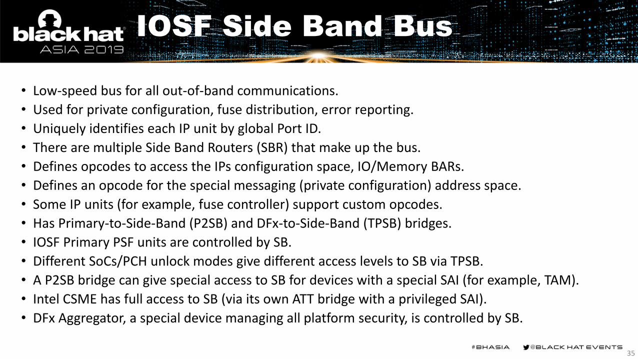
• Low-speed bus for all out-of-band communications.
• Used for private configuration, fuse distribution, error reporting.
• Uniquely identifies each IP unit by global Port ID.
• There are multiple Side Band Routers (SBR) that make up the bus.
• Defines opcodes to access the IPs configuration space, IO/Memory BARs.
• Defines an opcode for the special messaging (private configuration) address space.
• Some IP units (for example, fuse controller) support custom opcodes.
• Has Primary-to-Side-Band (P2SB) and DFx-to-Side-Band (TPSB) bridges.
• IOSF Primary PSF units are controlled by SB.
• Different SoCs/PCH unlock modes give different access levels to SB via TPSB.
• A P2SB bridge can give special access to SB for devices with a special SAI (for example, TAM).
• Intel CSME has full access to SB (via its own ATT bridge with a privileged SAI).
• DFx Aggregator, a special device managing all platform security, is controlled by SB.
35

IOSF example for LBG Chipset
Primary
Side Band
DFx
Buses
External
*IE Gasket has implied bridges
*
36

Demo
FUSEs
37

The Secrets of the Public Version of Intel System Studio
VISA
SoCHAP
TraceHub DCI (ExI)
Target
Host
ISSUSB
ODLA

Point of Interest
Intel System Studio Ultimate Trial Version (not available now???)
• Intel DAL
• Intel Debugging Tools
• Intel OpenIPC
• Intel System Trace
39
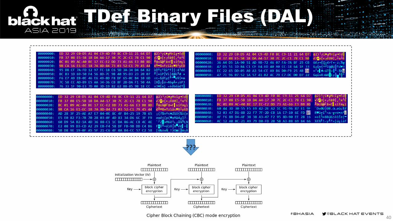
TDef Binary Files (DAL)
???
40
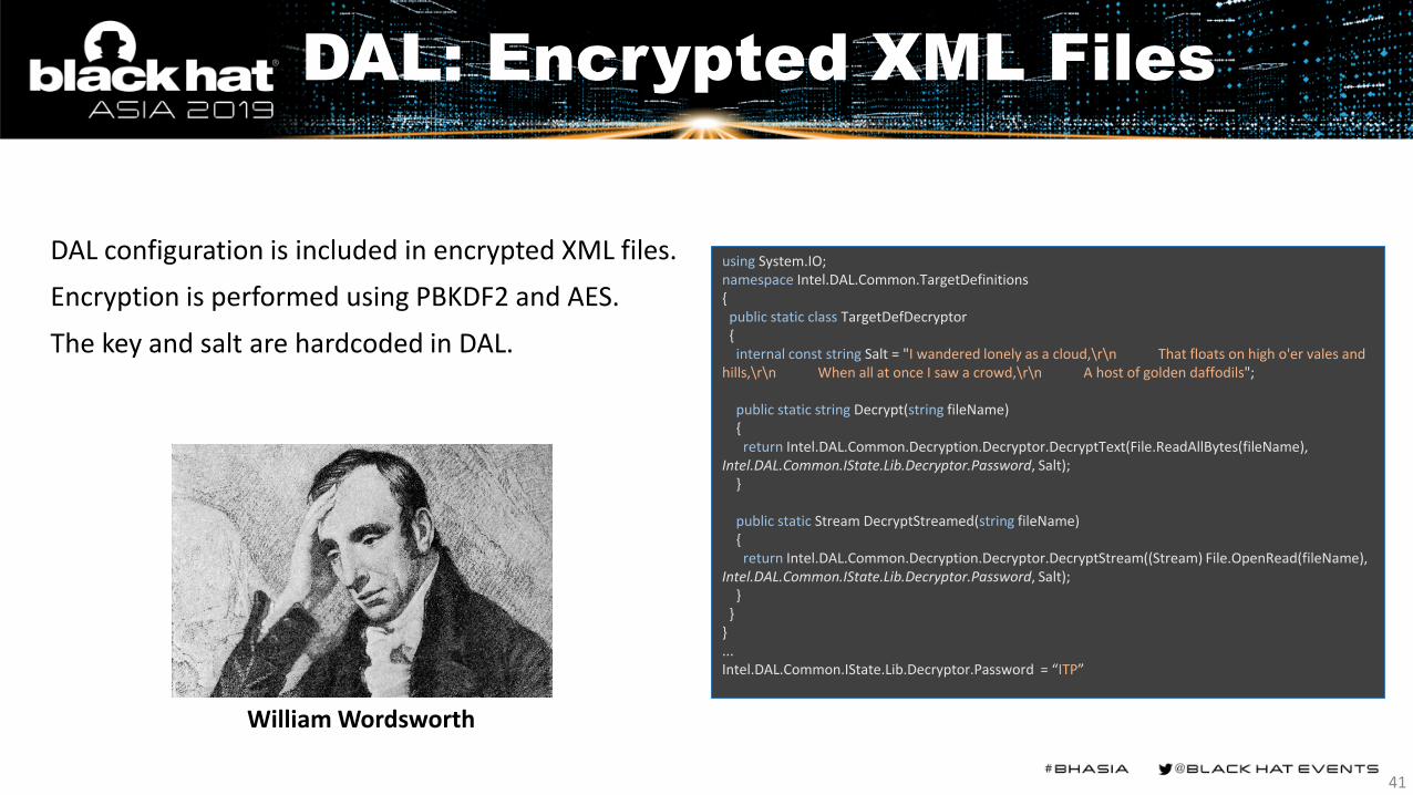
using System.IO;namespace Intel.DAL.Common.TargetDefinitions{
public static class TargetDefDecryptor{internal const string Salt = "I wandered lonely as a cloud,\r\n That floats on high o'er vales and
hills,\r\n When all at once I saw a crowd,\r\n A host of golden daffodils";
public static string Decrypt(string fileName){
return Intel.DAL.Common.Decryption.Decryptor.DecryptText(File.ReadAllBytes(fileName), Intel.DAL.Common.IState.Lib.Decryptor.Password, Salt);
}
public static Stream DecryptStreamed(string fileName){
return Intel.DAL.Common.Decryption.Decryptor.DecryptStream((Stream) File.OpenRead(fileName), Intel.DAL.Common.IState.Lib.Decryptor.Password, Salt);
}}
}...Intel.DAL.Common.IState.Lib.Decryptor.Password = “ITP”
DAL: Encrypted XML Files
DAL configuration is included in encrypted XML files.
Encryption is performed using PBKDF2 and AES.
The key and salt are hardcoded in DAL.
William Wordsworth
41

Our collection (DAL)DAL Version TDef size after
decryption (B)System Studio Version Platforms
1.9.3906 17,883,723 2014.0.026 AMT_MODULE, AVN, CLN, HSW, LMT, SLM_MODULE, SNB, VLV, VLV2
1.9.4772 7,375,914 2014.2.035 +TNG
1.9.5204 8,240,541 2015.0.027 +BDW, +IVB
1.9.5642 8,749,574 2015.1.039 +CHT
1.9.6202 49,999,719 2015.2.044, 2015.3.047, 2015.4.051 +ANN, CCK, HSX,IVT,JCK, JKT -CHT
1.9.7076 75,253,885 2016.0.024 +SKL, SPT
1.9.7302 75,254,918 2016.0.012 -
1.9.7438 75,273,050 2016.0.028, 2016.1.028 -
1.9.7622 76,037,659 2016.0.045 +BDX, BDXDE
1.9.7806 76,044,679 2016.2.040 -
1.9.7870 76,044,472 2016.0.050, 2016.3.043 -
1.9.8116 76,053,788 2016.0.053, 2016.0.057, 2016.4.046 -
1.9.8490 80,276,568 2017.0.039, 2017.1.045 +BDXDE_NS
1.9.g_8968 81,445,662 2017.2.050 +KBL, KBP
1.9.g_9114 81,026,115 2017.3.057 -
1.9.g_9490 82,952,952 2018b.0.0.028 +LBG, SKX
1.9.g_9588 86,433,780 2018.0.040, 2018.1.051, 2018.2.059 +CFL,CHT
1.1819.222.110 259,507,590 2019b.0.014 +CNP,+MCIVR
1.1831.340.110 297,853,487 2019.0.033 +CNL, WHL
1.1839.428.110 309,947,000 2019.1.050, 2019.2.057 +CMP42

Interesting Finds in XML

CPU FUSEs: With Sauce or Not?
<FuseDescriptor Bits="446:446" Name="fb_dun_ooo_dis_fuse" _description="Out of order Disabled" />...<FuseDescriptor Bits="679:673" Name="fus_thm_icaldatslope" _description="required for calibration value store - calibration fuses used for temperature slope" /><FuseDescriptor Bits="698:680" Name="fus_dpll_spare_fuses" _description="dpll spare fuse bits" /><FuseDescriptor Bits="699:699" Name="fus_bkend_secretsource" _description="Backend Secret Sauce bit: 0 : disable Secret Sauce 1 : enable Secret Sauce" /><FuseDescriptor Bits="700:700" Name="fus_dfx_scan_disable" _description="0 - enable DFX MBIST and scan mode 1 - disable DFX MBIST and scan mode" />
\dal_standalone_v1.9.3906\DAL\TDef\Devices\CLN\CLN_CLTAP\STAP_FUS\Fuse.xml
What is the "secret sauce bit" or "secret source bit"???
44

Deterministic Random Generator
\dal_standalone_v1.9.3906\DAL\TDef\Devices\HSW\HSW_UC\Fuse.A0.xml
<FuseDescriptor Bits="208:208" Name="RNG_DV_EN" _description="RNG Design Verification(DV) Enable. The usage model for this fuse is to blow it for units sent to testing organizations such as FIPS. Special testing specific microcode patches will be written and provided to FIPS so that they can dump out the output of" /><FuseDescriptor Bits="209:209" Name="RNG_DISABLE" _description="RNG Disable: Blowing this fuse will disable RNG functionality. Microcode will read the local copy of the fuse to enumerate the feature in CPUID (please see ucode in section 5.2, CPUID on page 20). When SW asks for a RDRAND when the feature is not avail" />...<FuseDescriptor Bits="669:669" Name="RNG_DETERMINISTIC" _description="RNG Deterministic Mode - The usage model for this fuse is to blow it for post-silicon SV testing for Intel internal use only. This would be provided to validation groups that need to test IVB units with the same microcode as production units or groups th" /><FuseDescriptor Bits="670:670" Name="RNG_FIPS_MODE" _description="FIPS mode. It is assumed that this will be blown for production parts. It is defined to mean that intervention to the functionality of the DRNG from external sources is disabled. For example, if it is blown, the test port will reset internal DRNG state" />
<FuseDescriptor Bits="464:464" Name="RNG_DV_EN" _description="RNG Design Verification(DV) Enable. The usage model for this fuse is to blow it for units sent to testing organizations such as FIPS. Special testing specific microcode patches will be written and provided to FIPS so that they can dump out the output of" /><FuseDescriptor Bits="465:465" Name="RNG_DISABLE" _description="RNG Disable: Blowing this fuse will disable RNG functionality. Microcode will read the local copy of the fuse to enumerate the feature in CPUID (please see ucode in section 5.2, CPUID on page 20). When SW asks for a RDRAND when the feature is not avail" />...<FuseDescriptor Bits="925:925" Name="RNG_DETERMINISTIC" _description="RNG Deterministic Mode - The usage model for this fuse is to blow it for post-silicon SV testing for Intel
internal use only. This would be provided to validation groups that need to test IVB units with the same microcode as production units or groups th" /><FuseDescriptor Bits="926:926" Name="RNG_FIPS_MODE" _description="FIPS mode. It is assumed that this will be blown for production parts. It is defined to mean that intervention to the functionality of the DRNG from external sources is disabled. For example, if it is blown, the test port will reset internal DRNG state" />
\dal_standalone_v1.9.3906\DAL\TDef\Devices\HSW\HSW_UC\Fuse.X0.xml
Deterministic Mode fuse for Hardware Random Generator
45

What about security?
How can you unlock arbitrary your platform?

Hardware Security Levels
Intel provides the following access levels: GREEN, ORANGE, RED, and WHITE(?)
47
Level JTAG CPU-core
(SoC, CPU)
JTAG ME-core
(SoC, PCH)
JTAG ISH-core
(SoC, PCH)
SB (Full)
(SoC, PCH)
JTAGUNCORE
(SoC, CPU)
VISA
(SoC, PCH,CPU)
Microcode
(SoC, CPU)
Purpose
RED + + + + + Full + Intel
WHITE(?) - - - - - Full - ???
ORANGE + -/* + - - Partial - Vendors
GREEN + - - - - -/Partial - Customer
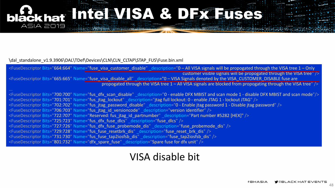
Intel VISA & DFx Fuses
<FuseDescriptor Bits="664:664" Name="fuse_visa_customer_disable" _description="0 – All VISA signals will be propogated through the VISA tree 1 – Only customer visible signals will be propogated through the VISA tree" />
<FuseDescriptor Bits="665:665" Name="fuse_visa_disable_all" _description="0 – VISA Signals denoted by the VISA_CUSTOMER_DISABLE fuse are propogated through the VISA tree 1 – All VISA signals are blocked from propogating through the VISA tree" />
...<FuseDescriptor Bits="700:700" Name="fus_dfx_scan_disable" _description="0 - enable DFX MBIST and scan mode 1 - disable DFX MBIST and scan mode"/><FuseDescriptor Bits="701:701" Name="fus_jtag_lockout" _description="jtag full lockout: 0 - enable JTAG 1 - lockout JTAG" /><FuseDescriptor Bits="702:702" Name="fus_jtag_password_disable" _description="0 - Enable jtag password 1 - Disable jtag password" /><FuseDescriptor Bits="706:703" Name="fus_jtag_id_versioncode" _description="version identifier" /><FuseDescriptor Bits="722:707" Name="Reserved: fus_jtag_id_partnumber" _description="Part number #5282 [HEX]" /><FuseDescriptor Bits="725:723" Name="fus_dfx_fuse_dlcs" _description="fuse_dlcs" /><FuseDescriptor Bits="727:726" Name="fus_dfx_fuse_probemode_dis" _description="fuse_probemode_dis" /><FuseDescriptor Bits="729:728" Name="fus_fuse_resetbrk_dis" _description="fuse_reset_brk_dis" /><FuseDescriptor Bits="731:730" Name="fus_fuse_tap2iosfsb_dis" _description="fuse_tap2iosfsb_dis" /><FuseDescriptor Bits="801:732" Name="dfx_spare_fuse" _description="Spare fuse for dfx unit" />
\dal_standalone_v1.9.3906\DAL\TDef\Devices\CLN\CLN_CLTAP\STAP_FUS\Fuse.bin.xml
VISA disable bit
48
Unlock Methods
1. Vulnerability
49
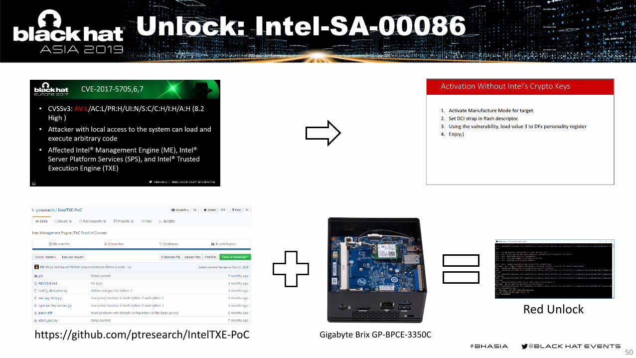
Unlock: Intel-SA-00086
https://github.com/ptresearch/IntelTXE-PoC Gigabyte Brix GP-BPCE-3350C
Red Unlock
50

Demo
Memory Tracing
51

Unlock: 1-days
52

Unlock Methods
2. Orange Mystery (TXE only)
53

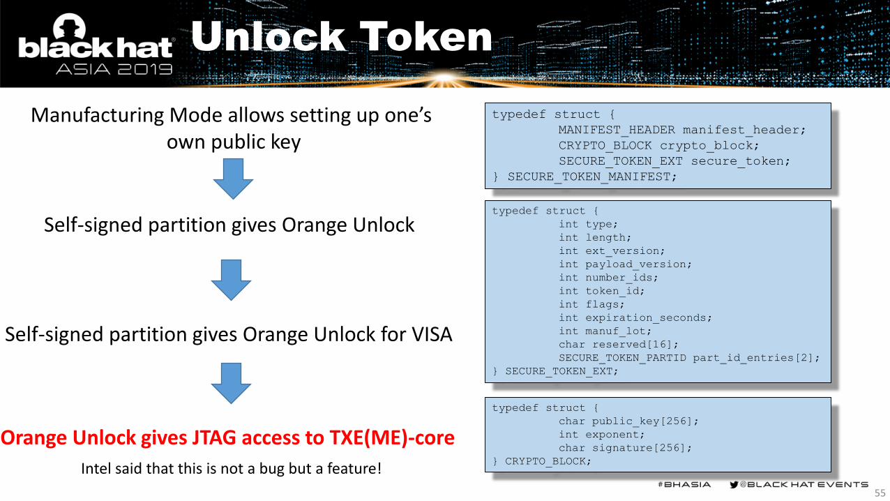
Unfused Key
Manufacturing Mode Unfused OEM Public key
54
Unlock Token
typedef struct {
MANIFEST_HEADER manifest_header;
CRYPTO_BLOCK crypto_block;
SECURE_TOKEN_EXT secure_token;
} SECURE_TOKEN_MANIFEST;
typedef struct {
char public_key[256];
int exponent;
char signature[256];
} CRYPTO_BLOCK;
typedef struct {
int type;
int length;
int ext_version;
int payload_version;
int number_ids;
int token_id;
int flags;
int expiration_seconds;
int manuf_lot;
char reserved[16];
SECURE_TOKEN_PARTID part_id_entries[2];
} SECURE_TOKEN_EXT;
Self-signed partition gives Orange Unlock
Self-signed partition gives Orange Unlock for VISA
Orange Unlock gives JTAG access to TXE(ME)-core
Intel said that this is not a bug but a feature!
Manufacturing Mode allows setting up one’sown public key
55

Unlock Methods
3. Intel JTAG Password
56

Unlock: Traffic Light Passwords
<_tdef deviceType="SKL_M_UC" tables="TapDefs"><_tdefDevice steppings="M0">
<TapDefs><TapCommands>
<TapCommand Ir="0x042" TapRegister="SA_TAP_LR_GLOBALUNLOCK" _name="SA_TAP_LR_GLOBALUNLOCK" Register="READWRITE" /><TapCommand Ir="0x048" TapRegister="SA_TAP_LR_REDUNLOCK" _name="SA_TAP_LR_REDUNLOCK" Register="READWRITE" PreScan="PackageAndC10Wakeup.Awake" /><TapCommand Ir="0x049" TapRegister="SA_TAP_LR_ORANGEUNLOCK" _name="SA_TAP_LR_ORANGEUNLOCK" Register="READWRITE" PreScan="PackageAndC10Wakeup.Awake" /><TapCommand Ir="0x04A" TapRegister="SA_TAP_LR_UNIQUEID" _name="SA_TAP_LR_UNIQUEID" Register="READ1" PreScan="PackageAndC10Wakeup.Awake" />
…
<TapRegister _indices="71:0" _map="" _name="SA_TAP_LR_REDUNLOCK"><_tag key="Visible" value="false" /><Field _map="71:0" _name="DR_PASSWORD" />
</TapRegister>
\DAL_1.1839.428.110\TDef\Devices\SKL\SKL_M_UC\TapCmdReg.Tap.SA.M0.xml
\TCI\2013.0.013\jtag.ini
[CE4200]datfile=jcs\ia7muxia7.jcsxdp3jtagtclk=10000000mcrgjtagtclk=4000000cpu#0=1,11,tci-jtag-gen-ia.dll,CE4200,HT0,Mastercpu#1=2,11,tci-jtag-gen-ia.dll,CE4200,HT1,Slave...STUB=jtag.inipasswd01=13,64,31passwd02=64,101,77,107,67,111,76,110,85 ;65 4D 6B 43 6F 4C 6E 55passwd03=13,2,0passwd04=16,2,2 ; make this 7,3 to enable the 8051 on secondary chain
57

JTAG Password FUSEs
<FuseDescriptor Bits="845:845" Name="fus_jtag_password_select" _description="Choose between static or dynamic password; 0-static password 1-dynamic password" />
\dal_standalone_v1.9.3906\DAL\TDef\Devices\CLN\CLN_CLTAP\STAP_FUS\Fuse.bin.xml
<FuseDescriptor Bits="12081:12072" Name="SAPF_COL_RED" _description="Display PF SRAM Column Redundancy" /><FuseDescriptor Bits="12087:12082" Name="security_spare" _description="spare but Security locked" /><FuseDescriptor Bits="12088:12088" Name="LR_FUSE_REG_KEY_ENABLE_FUSE_Orange_En" _description="" /><FuseDescriptor Bits="12089:12089" Name="LR_FUSE_REG_KEY_ENABLE_FUSE_Red_En" _description="" /><FuseDescriptor Bits="12090:12090" Name="LR_FUSE_REG_KEY_ENABLE_FUSE_Legacy_Disable" _description="" /><FuseDescriptor Bits="12091:12091" Name="LR_FUSE_REG_KEY_ENABLE_FUSE_Tap_Spare" _description="" /><FuseDescriptor Bits="12092:12092" Name="LOCKOUT_FUSE_HDCP_key" _description="Disable Programming of some fuses. This fuse is NOT override-able to prevent fuse programming after the lockout fuse is burnt." /><FuseDescriptor Bits="12093:12093" Name="LOCKOUT_FUSE_PAVP2_key" _description="Disable Programming of some fuses. This fuse is NOT override-able to prevent fuse programming after the lockout fuse is burnt." /><FuseDescriptor Bits="12094:12094" Name="LOCKOUT_FUSE_GLOB" _description="Disable Programming of some fuses. This fuse is NOT override-able to prevent fuse programming after the lockout fuse is burnt." /><FuseDescriptor Bits="12095:12095" Name="LOCKOUT_FUSE_spare" _description="" /><FuseDescriptor Bits="12159:12096" Name="LR_FUSE_REG_UNIQUEID_FUSE_UNIQUEID" _description="test" /><FuseDescriptor Bits="12223:12160" Name="LR_FUSE_REG_RED_KEY_FUSE_PASSWORD" _description="test" /><FuseDescriptor Bits="12287:12224" Name="LR_FUSE_REG_ORANGE_KEY_FUSE_PASSWORD" _description="test" />
\dal_standalone_v1.9.3906\DAL\TDef\Devices\HSW\HSW_UC\Fuse.A0.xml
58

JTAG Password Live Cycle
1. Request UID/Password
4. ResponseUID/Password
2. GenerateUID/Password
3. SaveUID/Password
FUSE station
ServerCPU/PCH
5. Programming UID/Hash(Password)
6. Request UID
7. Response UID
8. Request Password for UID
9. Authentication
10. Get Password from DB
11. Send Password
12. Unlock using password
Manufacturing
Debugging a public system Engineer Computer59
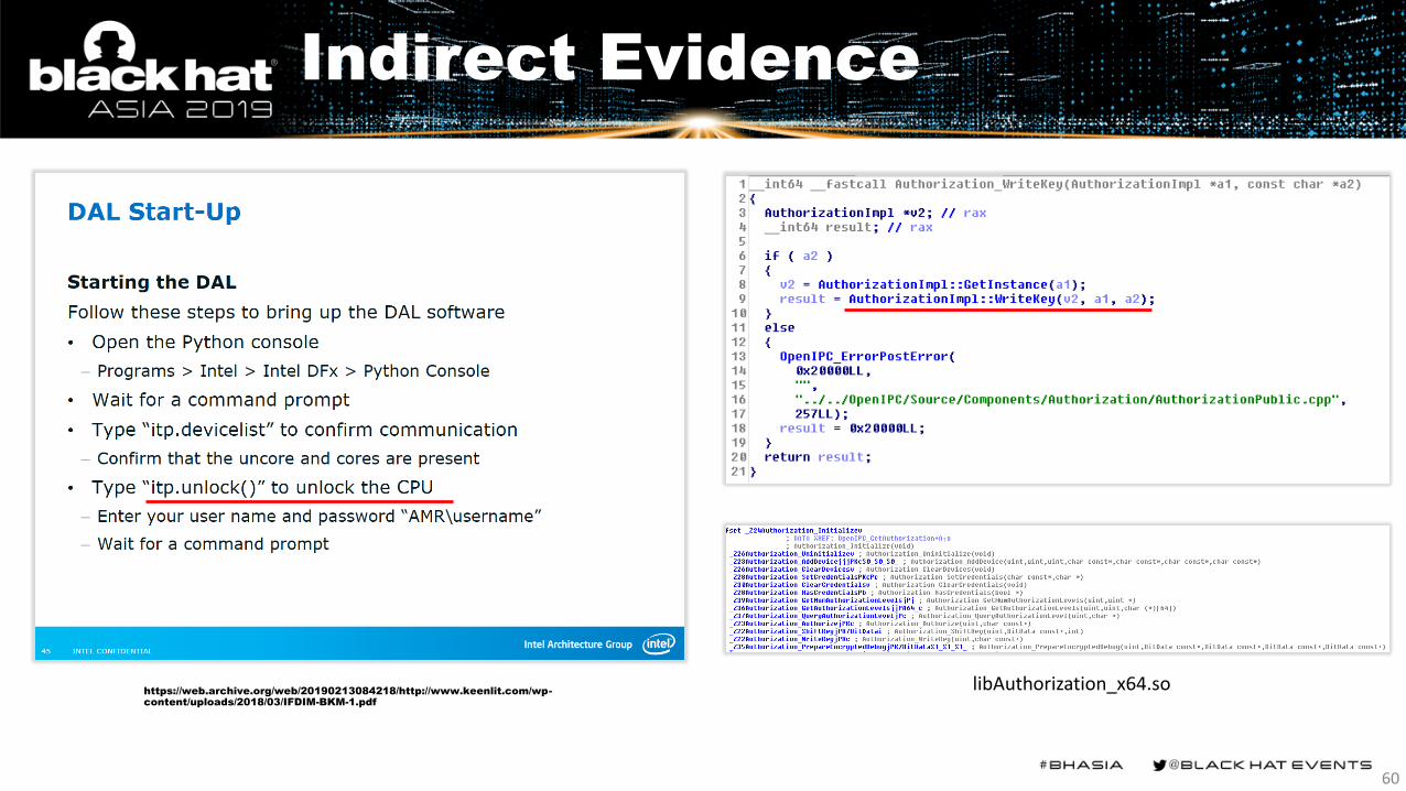
Indirect Evidence
https://web.archive.org/web/20190213084218/http://www.keenlit.com/wp-
content/uploads/2018/03/IFDIM-BKM-1.pdf
libAuthorization_x64.so
60

We didn’t manage to get the JTAG password for our platform,
but we think it is possible this way.
61

Unlock Methods
4. Hardware Way
62
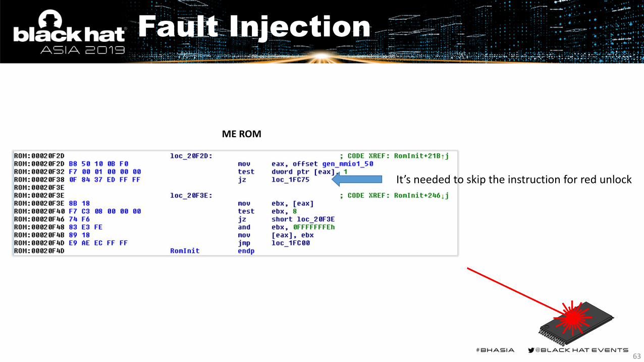
Fault Injection
It’s needed to skip the instruction for red unlock
ME ROM
63
Main Point
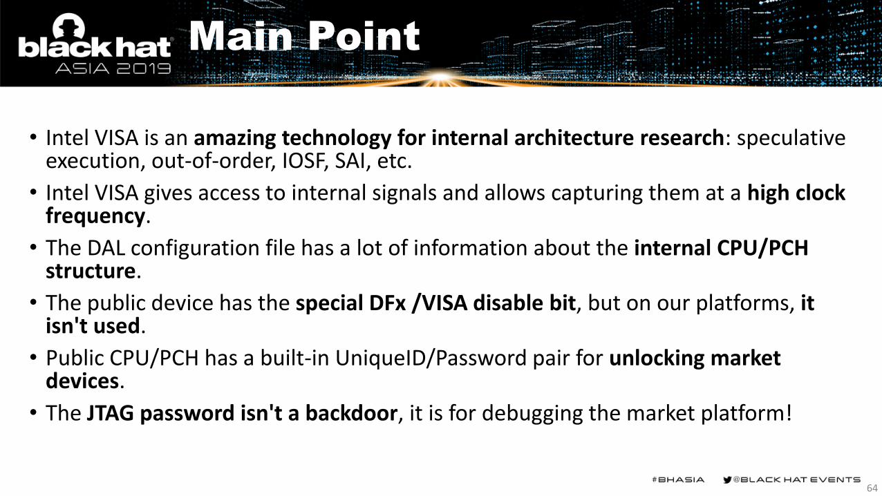
• Intel VISA is an amazing technology for internal architecture research: speculative execution, out-of-order, IOSF, SAI, etc.
• Intel VISA gives access to internal signals and allows capturing them at a high clock frequency.
• The DAL configuration file has a lot of information about the internal CPU/PCH structure.
• The public device has the special DFx /VISA disable bit, but on our platforms, it isn't used.
• Public CPU/PCH has a built-in UniqueID/Password pair for unlocking market devices.
• The JTAG password isn't a backdoor, it is for debugging the market platform!
64

Our Relative Papers
[1] Where there’s a JTAG, there’s a Way: Obtaining Full System Access via USB;
[2] How to Hack a Turned-Off Computer, or Running Unsigned Codein Intel Management Engine;
[3] Inside Intel Management Engine, 34c3;
[4] Intel ME: Security keys Genealogy, Obfuscation and other Magic;
[5] Intel ME Manufacturing Mode: obscured dangers and their relationship to Apple MacBook vulnerability CVE-2018-4251;
65

Thank you!Questions?
Mark Ermolov Maxim Goryachy@_markel__ @h0t_max
https://github.com/ptresearch
https://blog.ptsecurity.com
66
Bonus Slides

SB Port IDs for Louisburg (LBG) Chipset
BROADCAST1 = 0xFF,BROADCAST2 = 0xFE,DMI = 0xEF,ESPISPI = 0xEE,ICLK = 0xED,MODPHY4 = 0xEB,MODPHY5 = 0x10,MODPHY1 = 0xE9,PMC = 0xE8,XHCI = 0xE6,OTG = 0xE5,SPE = 0xE4,SPD = 0xE3,SPC = 0xE2,SPB = 0xE1,SPA = 0xE0,UPSX8 = 0x06,UPSX16 = 0x07,TAP2IOSFSB1 = 0xDF,TRSB = 0xDD,ICC = 0xDC,GBE = 0xDB,SATA = 0xD9,SSATA = 0x0F,LDO = 0x14,
LDO = 0x14,DSP = 0xD7,FUSE = 0xD5,FSPROX0 = 0xD4,DRNG = 0xD2,FIA = 0xCF,FIAWM26 = 0x13,USB2 = 0xCA,LPC = 0xC7,SMB = 0xC6,P2S = 0xC5,ITSS = 0xC4,RTC = 0xC3,PSF5 = 0x8F,PSF6 = 0x70,PSF7 = 0x01,PSF8 = 0x29,PSF9 = 0x21,PSF10 = 0x36,PSF4 = 0xBD,PSF3 = 0xBC,PSF2 = 0xBB,PSF1 = 0xBA,HOTHARM = 0xB9,DCI = 0xB8,DFXAGG = 0xB7,
NPK = 0xB6,MMP0 = 0xB0,GPIOCOM0 = 0xAF,GPIOCOM1 = 0xAE,GPIOCOM2 = 0xAD,GPIOCOM3 = 0xAC,GPIOCOM4 = 0xAB,GPIOCOM5 = 0x11,MODPHY2 = 0xA9,MODPHY3 = 0xA8,PNCRC = 0xA5,PNCRB = 0xA4,PNCRA = 0xA3,PNCR0 = 0xA2,CSME15 = 0x9F, //SMS2CSME14 = 0x9E, //SMS1CSME13 = 0x9D, //PMTCSME12 = 0x9C, //PTIOCSME11 = 0x9B, //PECICSME9 = 0x99, //SMT6CSME8 = 0x98, //SMT5CSME7 = 0x97, //SMT4CSME6 = 0x96, //SMT3CSME5 = 0x95, //SMT2CSME4 = 0x94, //SMT1
CSME3 = 0x93, //FSCCSME2 = 0x92, //USB-RSAICSME0 = 0x90, //CSECSME_PSF = 0x8F, //MEPSFCSMERTC = 0x8E,IEUART = 0x80,IEHOTHAM = 0x7F,IEPMT = 0x7E,IESSTPECI = 0x7D,IEFSC = 0x7C,IESMT5 = 0x7B,IESMT4 = 0x7A,IESMT3 = 0x79,IESMT2 = 0x78,IESMT1 = 0x77,IESMT0 = 0x76,IEUSBR = 0x74,IEPTIO = 0x73,IEIOSFGASKET = 0x72,IEPSF = 0x70,FPK = 0x0A,MP0KR = 0x3C,MP1KR = 0x3E,RUAUX = 0x0B,
RUMAIN = 0x3B,EC = 0x20,CPM2 = 0x38,CPM1 = 0x37,CPM0 = 0x0C,VSPTHERM = 0x25,VSPP2SB = 0x24,VSPFPK = 0x22,VSPCPM2 = 0x35,VSPCPM1 = 0x34,VSPCPM0 = 0x33,MSMROM = 0x08,PSTH = 0x89
68

Override-able Fuses
<FuseDescriptor Bits="12071:12056" Name="security_spare" _description="spare but Security locked" /><FuseDescriptor Bits="12075:12072" Name="LCP_DEFAULTS_core" _description="default value of core LCP" /><FuseDescriptor Bits="12079:12076" Name="LCP_DEFAULTS_llc" _description="default value of llc LCP" /><FuseDescriptor Bits="12083:12080" Name="LCP_DEFAULTS_ring" _description="default value of ring LCP" /><FuseDescriptor Bits="12087:12084" Name="LCP_DEFAULTS_sa" _description="default value of sa LCP" /><FuseDescriptor Bits="12088:12088" Name="LR_FUSE_REG_KEY_ENABLE_FUSE_Orange_En" _description="" /><FuseDescriptor Bits="12089:12089" Name="LR_FUSE_REG_KEY_ENABLE_FUSE_Red_En" _description="" /><FuseDescriptor Bits="12090:12090" Name="LR_FUSE_REG_KEY_ENABLE_FUSE_Legacy_Disable" _description="" /><FuseDescriptor Bits="12091:12091" Name="LR_FUSE_REG_KEY_ENABLE_FUSE_Tap_Spare" _description="" /><FuseDescriptor Bits="12092:12092" Name="LOCKOUT_FUSE_HDCP_key" _description="Disable Programming of some fuses. This fuse is NOT override-able to prevent fuse programming after the lockout fuse is burnt." /><FuseDescriptor Bits="12093:12093" Name="LOCKOUT_FUSE_PAVP2_key" _description="Disable Programming of some fuses. This fuse is NOT override-able to prevent fuse programming after the lockout fuse is burnt." /><FuseDescriptor Bits="12094:12094" Name="LOCKOUT_FUSE_GLOB" _description="Disable Programming of some fuses. This fuse is NOT override-able to prevent fuse programming after the lockout fuse is burnt." /><FuseDescriptor Bits="12095:12095" Name="LOCKOUT_FUSE_spare" _description="" /><FuseDescriptor Bits="12159:12096" Name="LR_FUSE_REG_UNIQUEID_FUSE_UNIQUEID" _description="test" /><FuseDescriptor Bits="12223:12160" Name="LR_FUSE_REG_RED_KEY_FUSE_PASSWORD" _description="test" /><FuseDescriptor Bits="12287:12224" Name="LR_FUSE_REG_ORANGE_KEY_FUSE_PASSWORD" _description="test" />
\dal_standalone_v1.9.3906\DAL\TDef\Devices\CLN\CLN_CLTAP\STAP_FUS\Fuse.bin.xml
Does it mean that other fuses are override-able???
69