Embed Size (px)
Citation preview
Intel® Stratix® 10 DX DeviceOverview
SubscribeSend Feedback
S10-DX-OVERVIEW | 2020.03.24Latest document on the web: PDF | HTML
Contents
1. Intel® Stratix® 10 DX Device Overview........................................................................... 31.1. Intel Stratix 10 DX Devices..................................................................................... 41.2. Intel Stratix 10 DX Features Summary..................................................................... 51.3. Intel Stratix 10 DX Block Diagram............................................................................71.4. Intel Stratix 10 DX Family Plan................................................................................ 8
1.4.1. Available Options..................................................................................... 101.5. Intel Hyperflex Core Architecture........................................................................... 111.6. Heterogeneous 3D SiP Transceiver Tiles.................................................................. 121.7. Intel Stratix 10 DX Transceivers.............................................................................12
1.7.1. Intel P-Tile Transceivers and Hard IP...........................................................121.7.2. Intel E-Tile Transceivers and Hard IP...........................................................13
1.8. Heterogeneous 3D Stacked HBM2 DRAM Memory..................................................... 131.9. External Memory and General Purpose I/O.............................................................. 141.10. Adaptive Logic Module (ALM)............................................................................... 161.11. Core Clocking.................................................................................................... 171.12. I/O PLLs........................................................................................................... 181.13. Internal Embedded Memory.................................................................................181.14. Variable Precision DSP Block................................................................................191.15. Hard Processor System (HPS).............................................................................. 21
1.15.1. Key Features of the Intel Stratix 10 HPS....................................................221.16. Power Management............................................................................................ 251.17. Device Configuration and Secure Device Manager (SDM)......................................... 251.18. Device Security..................................................................................................271.19. Configuration via Protocol Using PCI Express..........................................................281.20. Partial and Dynamic Reconfiguration..................................................................... 281.21. Fast Forward Compile......................................................................................... 281.22. Single Event Upset (SEU) Error Detection and Correction.........................................291.23. Document Revision History for the Intel Stratix 10 DX Device Overview.....................29
Contents
Intel® Stratix® 10 DX Device Overview Send Feedback
2
1. Intel® Stratix® 10 DX Device OverviewTargeting high-performance acceleration applications, increasingly used in Datacenter,Networking, Cloud Computing, and Test & Measurement markets, Intel® Stratix® 10DX FPGAs feature hard intellectual property blocks supporting both coherent and non-coherent protocol interfaces.
A low latency, high performance coherent interface is achieved when connecting theFPGA to selected Intel Xeon® Scalable Processors via Intel Ultra Path Interconnect(UPI), while the non-coherent interface takes advantage of any PCI Express* (PCIe)Gen4 capable device.
The FPGA's external memory capability now includes support for a new DDR-T soft IPmemory controller, allowing interfaces to attach up to 1 TB of high-performance,persistent Intel Optane™ PMem modules per controller, directly to the FPGAs GPIObanks.
In addition to supporting these interface protocols, the DX variant FPGAs also offerhard intellectual property blocks for 100 Gigabit Ethernet and DDR4 memory control,combined with a high-performance monolithic 14 nm FPGA fabric die, all inside asingle flip-chip FBGA package. Select Intel Stratix 10 DX devices include an integratedquad-core 64-bit Arm* Cortex*-A53 hard processor subsystem (HPS) on the fabricdie, or embedded 3D stacked High-Bandwidth (up to 512 GB/s) DRAM memory(HBM2) inside the package.
As part of the Intel Stratix 10 family, the DX variant devices feature other innovationssuch as the Intel Hyperflex™ core architecture, variable precision DSP blocks withhardened support for both floating-point and fixed-point operation, and advancedpackaging technology based on Intel Embedded Multi-die Interconnect Bridge (EMIB).
Important innovations in Intel Stratix 10 DX devices include:
• Intel Hyperflex core architecture delivering higher core performance compared toprevious generation high-performance FPGAs
• Manufactured using Intel high volume 14 nm tri-gate (FinFET) technology
• Intel Embedded Multi-die Interconnect Bridge (EMIB) packaging technology
• A soft IP memory controller and PHY supporting DDR-T to directly attach IntelOptane PMem modules to the FPGA, two to four controllers per FPGA, and rates upto 2400 megatransfers per second (one module per channel)
• Transceivers on separate heterogeneous tiles, supporting data rates up to 57.8gigabits per second (Gbps) Pulse Amplitude Modulation (PAM4) and 28.9 Gbpsnon-return-to-zero (NRZ) for chip-to-chip, chip-to-module, and backplane driving
• Hard PCI Express Gen4 x16 intellectual property blocks, with useful features suchas Endpoint and Root Port bifurcation modes, virtualization support for Single-RootI/O virtualization (SR-IOV), Virtual I/O device (VIRTIO), Intel Scalable I/OVirtualization (Intel Scalable IOV), and Transaction Layer bypass mode
S10-DX-OVERVIEW | 2020.03.24
Send Feedback
Intel Corporation. All rights reserved. Agilex, Altera, Arria, Cyclone, Enpirion, Intel, the Intel logo, MAX, Nios,Quartus and Stratix words and logos are trademarks of Intel Corporation or its subsidiaries in the U.S. and/orother countries. Intel warrants performance of its FPGA and semiconductor products to current specifications inaccordance with Intel's standard warranty, but reserves the right to make changes to any products and servicesat any time without notice. Intel assumes no responsibility or liability arising out of the application or use of anyinformation, product, or service described herein except as expressly agreed to in writing by Intel. Intelcustomers are advised to obtain the latest version of device specifications before relying on any publishedinformation and before placing orders for products or services.*Other names and brands may be claimed as the property of others.
ISO9001:2015Registered
• Hard Intel UPI intellectual property blocks in select devices, supporting HomeAgent soft IP
• Hard 100G Ethernet MAC, 100G Reed-Solomon forward error correction (FEC), andKP-FEC blocks
• 3D stacked High-Bandwidth DRAM Memory (HBM2) in select devices
• Monolithic core fabric with up to 2.8 million logic elements (LEs)
• Hard fixed-point and IEEE 754 compliant hard floating-point variable precisiondigital signal processing (DSP) blocks
• Hard memory controllers and PHY supporting DDR4 rates up to 2666 megabits persecond (Mbps) per pin
• Hard HBM2 memory controllers in devices that include in-package 3D stackedHBM2 DRAM memory
• M20K, 20 kilobit (Kb) internal SRAM memory blocks
• eSRAM, 47.25 megabit (Mb) internal SRAM blocks in select devices
• Quad-core 64-bit Arm Cortex-A53 embedded processor running up to 1.5 GHz inselect devices, processor subsystem peripherals, and high bandwidth buses to andfrom the FPGA logic fabric
• Programmable clock tree synthesis for flexible, low power, low skew clock trees
• Dedicated Secure Device Manager (SDM) for enhanced device configuration andsecurity, supporting AES-256, SHA-256/384 and elliptic curve digital signaturealgorithm (ECDSA) -256/384 encrypt/decrypt accelerators, and multi-factorauthentication
• Comprehensive set of advanced power saving features
1.1. Intel Stratix 10 DX Devices
In addition to the coherent and non-coherent protocol interfaces that are required forhigh-performance acceleration applications, Intel Stratix 10 DX FPGAs deliverimproved core logic performance compared to previous generation high-performanceFPGAs, with densities up to 2.8 million LEs in a monolithic fabric.
The devices also feature up to 84 full-duplex transceivers on separate transceiver tiles,a subset of which are capable of supporting data rates up to 57.8 Gbps PAM4 and 28.9Gbps NRZ for both short reach and backplane driving applications. External memoryinterfaces up to 2666 Mbps DDR4 are achieved using hard memory controllers, andsome DX variant devices include in-package 3D stacked HBM2 DRAM memory capableof supporting 512 GByte/s memory bandwidth. Select devices contain an embeddedhard processor system (HPS) based on an application-class quad-core 64-bit ArmCortex-A53, running at clock rates up to 1.5 GHz, including processor peripherals andhigh-bandwidth buses to and from the FPGA logic fabric.
1. Intel® Stratix® 10 DX Device Overview
S10-DX-OVERVIEW | 2020.03.24
Intel® Stratix® 10 DX Device Overview Send Feedback
4
The high-performance monolithic FPGA fabric is based on the Intel Hyperflex corearchitecture that includes additional Hyper-Registers everywhere throughout theinterconnect routing and at the inputs of all functional blocks. The core fabric alsocontains an enhanced logic array utilizing Intel’s adaptive logic module (ALM) and arich set of high-performance building blocks including:
• M20K, 20 Kb embedded SRAM memory blocks
• eSRAM, 47.25 Mb embedded SRAM memory blocks (in select devices)
• Variable precision DSP blocks with hard fixed point and IEEE 754 compliant hardfloating-point
• General purpose IO cells with integer PLLs in every IO bank
• Hard memory controllers and PHY for external memory interfaces
• Hard memory controllers for in-package 3D stacked HBM2 DRAM memory (inselect devices)
To clock these fabric building blocks, Intel Stratix 10 DX FPGAs use programmableclock tree synthesis, which uses dedicated clock tree routing to synthesize only thosebranches of the clock trees required for the application.
The high-speed serial transceivers contain both the physical medium attachment(PMA) and the physical coding sublayer (PCS) required to implement a variety ofindustry standard protocols. In addition to the hard PCS for each transceiver, IntelStratix 10 DX devices contain hard PCI Express IP that supports up to Gen4 x16 laneconfiguration, hard Intel UPI IP in select devices that supports Home Agent soft IP,and hard 10/25/100 Gbps Ethernet MAC IP with dedicated Reed-Solomon FEC for NRZsignals (528, 514) and PAM4 signals (544, 514). These hardened intellectual propertyblocks free up valuable core logic resources, save power, and increase yourproductivity.
All Intel Stratix 10 DX devices support in-system, fine-grained partial reconfigurationof the logic array, allowing logic add and subtract from the system while it isoperating.
1.2. Intel Stratix 10 DX Features Summary
Table 1. Intel Stratix 10 DX Device Features
Feature Description
Configuration • Dedicated Secure Device Manager• Software programmable device configuration• Serial and parallel flash interface• Configuration via protocol (CvP) using PCI Express Gen1/Gen2/Gen3/Gen4• Fine-grained partial reconfiguration of core fabric• Dynamic reconfiguration of transceivers and PLLs• Comprehensive set of security features including AES-256, SHA-256/384, and
ECDSA-256/384 accelerators, and multi-factor authentication• Physically Unclonable Function (PUF) service
Core clock networks • Programmable clock tree synthesis, backwards compatible with global, regional andperipheral clock networks
• Clocks only synthesized where needed, to minimize dynamic power• 667 MHz external memory interface clocking, supports 2666 Mbps DDR4 interface• 800 MHz LVDS interface clocking, supports 1600 Mbps LVDS interface
continued...
1. Intel® Stratix® 10 DX Device Overview
S10-DX-OVERVIEW | 2020.03.24
Send Feedback Intel® Stratix® 10 DX Device Overview
5
Feature Description
Core process technology • 14 nm Intel tri-gate (FinFET) process technology• SmartVID controlled core voltage, standard power devices
Embedded hard IP • PCIe* Gen1/Gen2/Gen3/Gen4 x16 complete protocol stack, endpoint and root portbifurcation, SR-IOV, VIRTIO, Intel Scalable IOV, and Transaction Layer bypass
• Intel UPI hard IP requires Intel soft IP (separate licensing required, selected customersonly, 1SD210 and 1SD280 devices only)
• 100 GbE MAC, Reed-Solomon FEC hard IP, and KP-FEC hard IP• DDR4/DDR3 hard memory controller (RLDRAM3/QDR II+/QDR IV using soft memory
controller)• HBM2 DRAM hard memory controller (select devices)• Hard Processor system, Quad-core 64-bit Arm Cortex-A53 (select devices)
General purpose I/Os • Up to 816 total GPIO available• 1.6 Gbps LVDS—every pair can be configured as an input or output• Up to 2400 megatransfers per second DDR-T external memory interface (Intel soft IP
license required)• 1333 MHz/2666 Mbps DDR4 external memory interface• 1067 MHz/2133 Mbps DDR3 external memory interface• 1.2 V to 1.8 V single-ended LVCMOS/LVTTL interfacing• On-chip termination (OCT)
High performance monolithiccore fabric
• Intel Hyperflex core architecture with Hyper-Registers everywhere throughout theinterconnect routing and at the inputs of all functional blocks
• Monolithic fabric minimizes compile times and increases logic utilization• Enhanced adaptive logic module (ALM)• Improved multi-rack routing architecture reduces congestion and improves compile
times• Hierarchical core clocking architecture with programmable clock tree synthesis• Fine-grained partial reconfiguration
Internal memory blocks • eSRAM—47.25 Mbit with hard ECC support (select devices)• M20K—20 Kbit with hard ECC support• MLAB—640 bit distributed LUTRAM
Low power serialtransceivers
• Up to 84 total transceivers available• Continuous operating range of 1 Gbps to 57.8 Gbps PAM4 and 28.9 Gbps NRZ (E-tile
transceivers)• Backplane support up to 57.8 Gbps PAM4 and 28.9 Gbps NRZ (E-tile transceivers)• Transmit pre-emphasis and de-emphasis• Dynamic partial reconfiguration of individual transceiver channels• On-chip instrumentation (Eye Viewer non-intrusive data eye monitoring)
Packaging • Intel Embedded Multi-die Interconnect Bridge (EMIB) packaging technology• 1.0 mm ball-pitch FBGA packaging• Lead and lead-free package options
Phase locked loops (PLLs) • Integer PLLs adjacent to general purpose I/Os, support external memory, and LVDSinterfaces, clock delay compensation, zero delay buffering
Power management • SmartVID controlled core voltage, standard power devices• Intel Quartus® Prime Pro Edition integrated power analysis
Software and tools • Intel Quartus Prime Pro Edition design suite with new compiler and Hyper-Aware designflow
• Fast Forward compiler to allow Intel Hyperflex architecture performance exploration• Transceiver toolkit
continued...
1. Intel® Stratix® 10 DX Device Overview
S10-DX-OVERVIEW | 2020.03.24
Intel® Stratix® 10 DX Device Overview Send Feedback
6
Feature Description
• Platform Designer system integration tool• DSP Builder system integration tool• OpenCL* support
Variable precision DSPblocks
• IEEE 754-compliant hard single-precision floating point capability• Supports signal processing with precision ranging from 18x19 up to 54x54• Native 27x27 and 18x19 multiply modes• 64-bit accumulator and cascade for systolic FIRs• Internal coefficient memory banks• Pre-adder/subtractor improves efficiency• Additional pipeline register increases performance and reduces power
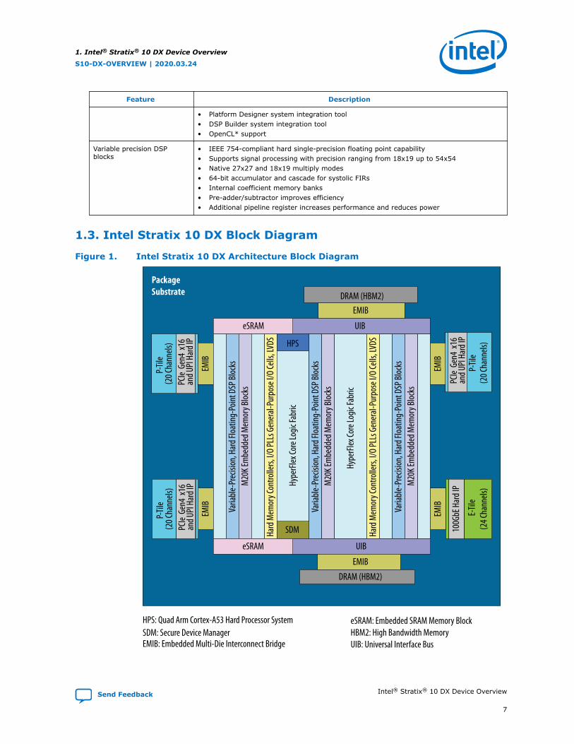
1.3. Intel Stratix 10 DX Block Diagram
Figure 1. Intel Stratix 10 DX Architecture Block Diagram
EMIB
P-Til
e(2
0 Cha
nnels
)
EMIB
Varia
ble-P
recis
ion, H
ard F
loatin
g-Po
int D
SP Bl
ocks
M20
K Em
bedd
ed M
emor
y Bloc
ks
Hard
Mem
ory C
ontro
llers,
I/O
PLLs
Gen
eral-
Purp
ose I
/O Ce
lls, L
VDS
Hype
rFlex
Core
Logic
Fabr
ic
Varia
ble-P
recis
ion, H
ard F
loatin
g-Po
int D
SP Bl
ocks
M20
K Em
bedd
ed M
emor
y Bloc
ks
Hype
rFlex
Core
Logic
Fabr
ic
SDM Hard
Mem
ory C
ontro
llers,
I/O
PLLs
Gen
eral-
Purp
ose I
/O Ce
lls, L
VDS
Varia
ble-P
recis
ion, H
ard F
loatin
g-Po
int D
SP Bl
ocks
M20
K Em
bedd
ed M
emor
y Bloc
ks
E-Til
e(2
4 Cha
nnels
)
100G
bE H
ard I
P
EMIB
EMIB
PackageSubstrate
SDM: Secure Device ManagerEMIB: Embedded Multi-Die Interconnect Bridge
eSRAM: Embedded SRAM Memory BlockHBM2: High Bandwidth MemoryUIB: Universal Interface Bus
UIBeSRAM
EMIBDRAM (HBM2)
UIBeSRAM
EMIB
DRAM (HBM2)
PCIe
Gen
4 x1
6 HPS
HPS: Quad Arm Cortex-A53 Hard Processor System
and U
PI H
ard I
P
P-Til
e(2
0 Cha
nnels
)PC
Ie G
en4
x16
and U
PI H
ard I
P
P-Til
e(2
0 Cha
nnels
)
PCIe
Gen
4 x1
6an
d UPI
Har
d IP
1. Intel® Stratix® 10 DX Device Overview
S10-DX-OVERVIEW | 2020.03.24
Send Feedback Intel® Stratix® 10 DX Device Overview
7
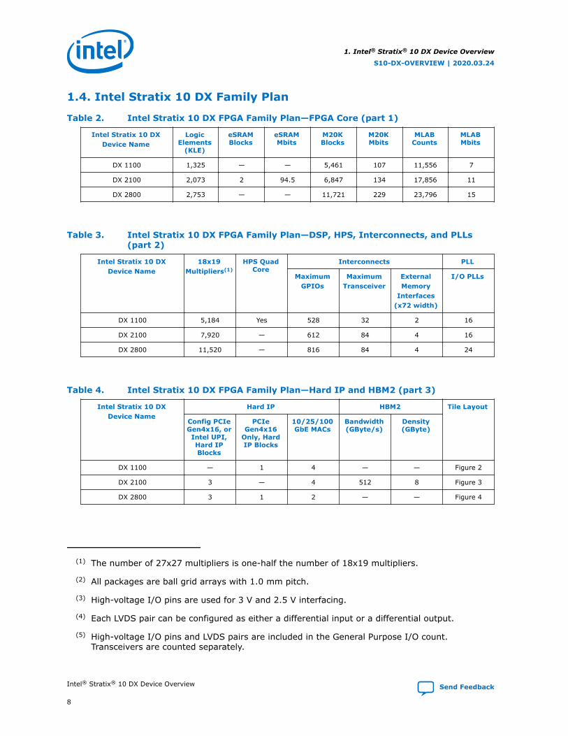
1.4. Intel Stratix 10 DX Family Plan
Table 2. Intel Stratix 10 DX FPGA Family Plan—FPGA Core (part 1)
Intel Stratix 10 DXDevice Name
LogicElements
(KLE)
eSRAMBlocks
eSRAMMbits
M20KBlocks
M20KMbits
MLABCounts
MLABMbits
DX 1100 1,325 — — 5,461 107 11,556 7
DX 2100 2,073 2 94.5 6,847 134 17,856 11
DX 2800 2,753 — — 11,721 229 23,796 15
Table 3. Intel Stratix 10 DX FPGA Family Plan—DSP, HPS, Interconnects, and PLLs(part 2)
Intel Stratix 10 DXDevice Name
18x19Multipliers(1)
HPS QuadCore
Interconnects PLL
MaximumGPIOs
MaximumTransceiver
ExternalMemory
Interfaces(x72 width)
I/O PLLs
DX 1100 5,184 Yes 528 32 2 16
DX 2100 7,920 — 612 84 4 16
DX 2800 11,520 — 816 84 4 24
Table 4. Intel Stratix 10 DX FPGA Family Plan—Hard IP and HBM2 (part 3)
Intel Stratix 10 DXDevice Name
Hard IP HBM2 Tile Layout
Config PCIeGen4x16, orIntel UPI,Hard IPBlocks
PCIeGen4x16
Only, HardIP Blocks
10/25/100GbE MACs
Bandwidth(GByte/s)
Density(GByte)
DX 1100 — 1 4 — — Figure 2
DX 2100 3 — 4 512 8 Figure 3
DX 2800 3 1 2 — — Figure 4
(1) The number of 27x27 multipliers is one-half the number of 18x19 multipliers.
(2) All packages are ball grid arrays with 1.0 mm pitch.
(3) High-voltage I/O pins are used for 3 V and 2.5 V interfacing.
(4) Each LVDS pair can be configured as either a differential input or a differential output.
(5) High-voltage I/O pins and LVDS pairs are included in the General Purpose I/O count.Transceivers are counted separately.
1. Intel® Stratix® 10 DX Device Overview
S10-DX-OVERVIEW | 2020.03.24
Intel® Stratix® 10 DX Device Overview Send Feedback
8
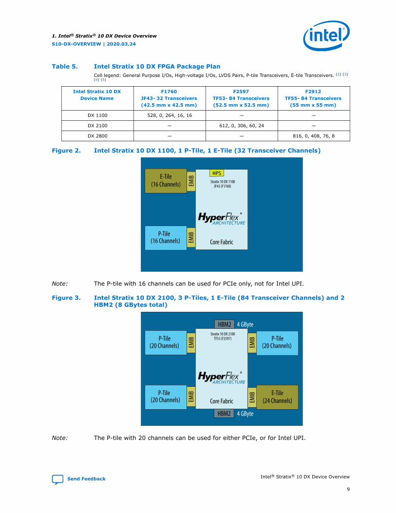
Table 5. Intel Stratix 10 DX FPGA Package PlanCell legend: General Purpose I/Os, High-voltage I/Os, LVDS Pairs, P-tile Transceivers, E-tile Transceivers. (2) (3)(4) (5)
Intel Stratix 10 DXDevice Name
F1760JF43- 32 Transceivers(42.5 mm x 42.5 mm)
F2597TF53- 84 Transceivers(52.5 mm x 52.5 mm)
F2912TF55- 84 Transceivers
(55 mm x 55 mm)
DX 1100 528, 0, 264, 16, 16 — —
DX 2100 — 612, 0, 306, 60, 24 —
DX 2800 — — 816, 0, 408, 76, 8
Figure 2. Intel Stratix 10 DX 1100, 1 P-Tile, 1 E-Tile (32 Transceiver Channels)
EMIB
EMIB
Core Fabric
®
Stratix 10 DX 1100 JF43 (F1760)
E-Tile(16 Channels)
P-Tile(16 Channels)
HPS
Note: The P-tile with 16 channels can be used for PCIe only, not for Intel UPI.
Figure 3. Intel Stratix 10 DX 2100, 3 P-Tiles, 1 E-Tile (84 Transceiver Channels) and 2HBM2 (8 GBytes total)
EMIB
EMIB
Core Fabric
®
Stratix 10 DX 2100
EMIB
TF53 (F2597)
E-Tile(24 Channels)
P-Tile(20 Channels)EM
IB
P-Tile(20 Channels)
P-Tile(20 Channels)
HBM2
HBM2 4 GByte
4 GByte
Note: The P-tile with 20 channels can be used for either PCIe, or for Intel UPI.
1. Intel® Stratix® 10 DX Device Overview
S10-DX-OVERVIEW | 2020.03.24
Send Feedback Intel® Stratix® 10 DX Device Overview
9
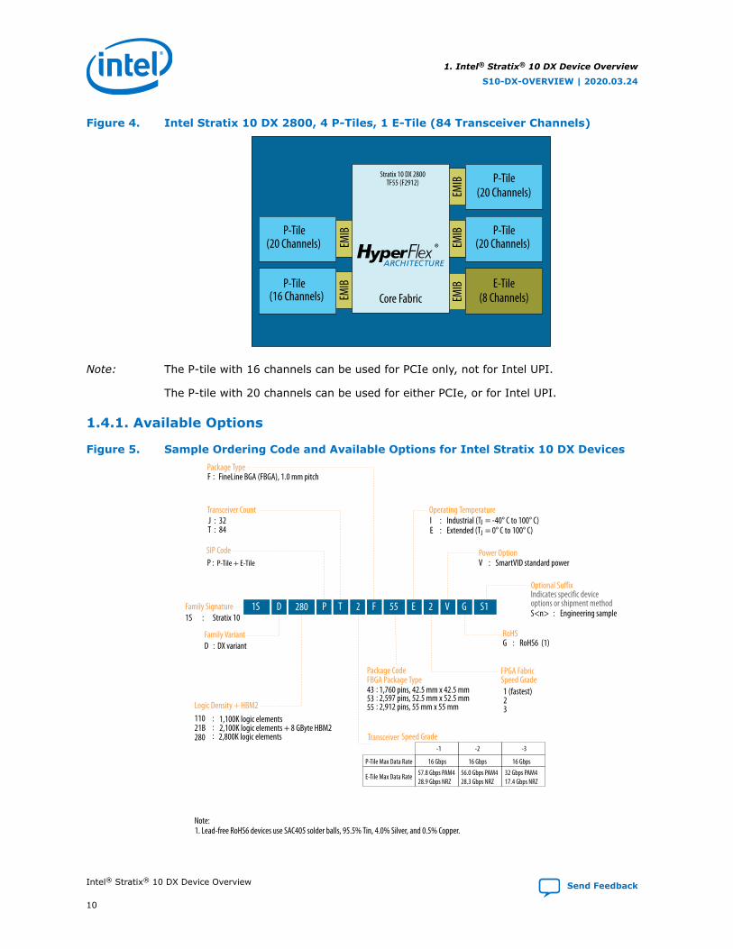
Figure 4. Intel Stratix 10 DX 2800, 4 P-Tiles, 1 E-Tile (84 Transceiver Channels)
EMIB
EMIB
Core Fabric
®
Stratix 10 DX 2800 P-Tile(20 Channels)EM
IBEM
IB
TF55 (F2912)
E-Tile(8 Channels)
P-Tile(20 Channels)EM
IB
P-Tile(16 Channels)
P-Tile(20 Channels)
Note: The P-tile with 16 channels can be used for PCIe only, not for Intel UPI.
The P-tile with 20 channels can be used for either PCIe, or for Intel UPI.
1.4.1. Available Options
Figure 5. Sample Ordering Code and Available Options for Intel Stratix 10 DX Devices
Family Signature
Transceiver Count
Transceiver Speed Grade
Package Type
Operating Temperature
FPGA Fabric Speed Grade
Optional SuffixIndicates specific device options or shipment method
D : DX variant
1S : Stratix 10
110 : 1,100K logic elements
J : 32T : 84
I : Industrial (TJ = -40° C to 100° C)
1 (fastest)23
Power OptionV : SmartVID standard power
RoHSG : RoHS6 (1)
S<n> : Engineering sample1S D F280 T 2 255 E S1V
Logic Density + HBM2
Family Variant
21B : 2,100K logic elements + 8 GByte HBM2
P
SIP CodeP :
Note:
P-Tile + E-Tile
P-Tile Max Data Rate
E-Tile Max Data Rate
-1 -2
16 Gbps 16 Gbps 16 Gbps
57.8 Gbps PAM428.9 Gbps NRZ
56.0 Gbps PAM428.3 Gbps NRZ
32 Gbps PAM417.4 Gbps NRZ
FBGA Package Type43
:
1,760 pins, 42.5 mm x 42.5 mm53
:
2,597 pins, 52.5 mm x 52.5 mm
G
-3280 : 2,800K logic elements
F : FineLine BGA (FBGA), 1.0 mm pitch
55 : 2,912 pins, 55 mm x 55 mm
Package Code
E : Extended (TJ = 0° C to 100° C)
1. Lead-free RoHS6 devices use SAC405 solder balls, 95.5% Tin, 4.0% Silver, and 0.5% Copper.
1. Intel® Stratix® 10 DX Device Overview
S10-DX-OVERVIEW | 2020.03.24
Intel® Stratix® 10 DX Device Overview Send Feedback
10
1.5. Intel Hyperflex Core Architecture
Intel Stratix 10 DX devices are based on a monolithic core fabric featuring the newIntel Hyperflex core architecture. The Intel Hyperflex core architecture delivers higherperformance and up to 70% lower power compared to previous generation high-endFPGAs. Along with this performance breakthrough, the Intel Hyperflex corearchitecture delivers a number of advantages including:
• Higher Throughput—Capitalizes on high core clock frequency performance toobtain throughput breakthroughs
• Improved Power Efficiency—Uses reduced IP size, enabled by Intel Hyperflex,to consolidate designs which previously spanned multiple devices into a singledevice, thereby reducing power by up to 70% versus previous generation devices
• Greater Design Functionality—Uses faster clock frequency to reduce bus widthsand reduce IP size, freeing up additional FPGA resources to add greaterfunctionality
• Increased Designer Productivity—Boosts performance with less routingcongestion and fewer design iterations using Hyper-Aware design tools, obtaininggreater timing margin for more rapid timing closure
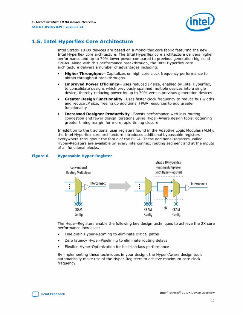
In addition to the traditional user registers found in the Adaptive Logic Modules (ALM),the Intel Hyperflex core architecture introduces additional bypassable registerseverywhere throughout the fabric of the FPGA. These additional registers, calledHyper-Registers are available on every interconnect routing segment and at the inputsof all functional blocks.
Figure 6. Bypassable Hyper-Register
clk CRAMConfig
CRAMConfig
CRAMConfig
InterconnectInterconnect
Stratix 10 HyperFlexRouting Multiplexer
(with Hyper-Register)Conventional
Routing Multiplexer
The Hyper-Registers enable the following key design techniques to achieve the 2X coreperformance increases:
• Fine grain Hyper-Retiming to eliminate critical paths
• Zero latency Hyper-Pipelining to eliminate routing delays
• Flexible Hyper-Optimization for best-in-class performance
By implementing these techniques in your design, the Hyper-Aware design toolsautomatically make use of the Hyper-Registers to achieve maximum core clockfrequency.
1. Intel® Stratix® 10 DX Device Overview
S10-DX-OVERVIEW | 2020.03.24
Send Feedback Intel® Stratix® 10 DX Device Overview
11
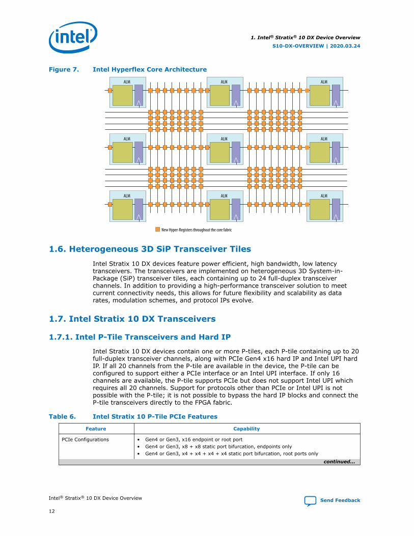
Figure 7. Intel Hyperflex Core Architecture
ALM ALM ALM
ALM ALM ALM
ALM ALM ALM
New Hyper-Registers throughout the core fabric
1.6. Heterogeneous 3D SiP Transceiver Tiles
Intel Stratix 10 DX devices feature power efficient, high bandwidth, low latencytransceivers. The transceivers are implemented on heterogeneous 3D System-in-Package (SiP) transceiver tiles, each containing up to 24 full-duplex transceiverchannels. In addition to providing a high-performance transceiver solution to meetcurrent connectivity needs, this allows for future flexibility and scalability as datarates, modulation schemes, and protocol IPs evolve.
1.7. Intel Stratix 10 DX Transceivers
1.7.1. Intel P-Tile Transceivers and Hard IP
Intel Stratix 10 DX devices contain one or more P-tiles, each P-tile containing up to 20full-duplex transceiver channels, along with PCIe Gen4 x16 hard IP and Intel UPI hardIP. If all 20 channels from the P-tile are available in the device, the P-tile can beconfigured to support either a PCIe interface or an Intel UPI interface. If only 16channels are available, the P-tile supports PCIe but does not support Intel UPI whichrequires all 20 channels. Support for protocols other than PCIe or Intel UPI is notpossible with the P-tile; it is not possible to bypass the hard IP blocks and connect theP-tile transceivers directly to the FPGA fabric.
Table 6. Intel Stratix 10 P-Tile PCIe Features
Feature Capability
PCIe Configurations • Gen4 or Gen3, x16 endpoint or root port• Gen4 or Gen3, x8 + x8 static port bifurcation, endpoints only• Gen4 or Gen3, x4 + x4 + x4 + x4 static port bifurcation, root ports only
continued...
1. Intel® Stratix® 10 DX Device Overview
S10-DX-OVERVIEW | 2020.03.24
Intel® Stratix® 10 DX Device Overview Send Feedback
12
Feature Capability
• Gen2 and Gen1 configurations supported indirectly through link negotiation• x1, x2 widths supported indirectly through protocol width reduction capability• Chip-to-chip and low-loss cable support
Virtualization Support • Single-Root I/O Virtualization (SR-IOV), 8 physical functions (PF) and 2048 virtualfunctions (VF) per endpoint
• Intel Scalable IOV support for software-based virtualization• Virtual I/O Device (VIRTIO)
Switch Support • Transaction Layer Bypass (TLP bypass) enables PCIe switch implementations usingSWUP and SWDN ports
Table 7. Intel Stratix 10 P-Tile Intel UPI Features
Feature Capability
Intel UPI Configurations • 20 lane support for 9.6 GT/s, 10.4 GT/s, 11.2 GT/s data rates• PHY and Link Layer support for Home Agent soft IP, Home Agent is implemented in the
FPGA fabric• Chip-to-chip and low-loss cable support
1.7.2. Intel E-Tile Transceivers and Hard IP
Intel Stratix 10 DX devices contain one E-tile.
Each E-tile contains up to 24 full-duplex dual-mode transceivers, each transceivercapable of supporting both Pulse Amplitude Modulation with 4 levels (PAM4) up to57.8 Gbps, and non-return-to-zero (NRZ) up to 28.9 Gbps. In addition to thetransceivers, each E-tile contains multiple instances of 10/25/100 Gbps Ethernet MAC+ FEC hard IP blocks. Both Reed-Solomon and KP FEC hard IP blocks are included,allowing complete Ethernet interfaces to be implemented, simplifying the design ofcomplex multi-port Ethernet systems.
Table 8. Available E-Tile Transceiver Channels in Intel Stratix 10 DX FPGA Devices
Intel Stratix 10 DX DeviceName
Number of E-TileTransceiver Channels
Available E-Tile Transceiver Channel Locations
DX 1100 16 0, 1, 2, 3, 8, 9, 10, 11, 12, 13, 14, 15, 20, 21, 22, 23
DX 2100 24 0 through 23
DX 2800 8 0, 1, 2, 3, 12, 13, 14, 15
For more information about the E-tile transceivers and the E-tile Ethernet hard IP,refer to the Intel Stratix 10 E-Tile Transceiver PHY User Guide.
1.8. Heterogeneous 3D Stacked HBM2 DRAM Memory
Select Intel Stratix 10 DX devices integrate 3D stacked High-Bandwidth DRAM Memory(HBM2) alongside a high-performance monolithic 14 nm FPGA fabric die, and multiplehigh-speed transceiver tiles, all inside a single flip-chip FBGA package.
This results in a “near memory” implementation where the high-density stacked DRAMis integrated very close to the FPGA in the same package. In this configuration the in-package memory is able to deliver up to 512 GByte/s of total aggregate bandwidthwhich represents over a 10X increase in bandwidth compared to traditional “far
1. Intel® Stratix® 10 DX Device Overview
S10-DX-OVERVIEW | 2020.03.24
Send Feedback Intel® Stratix® 10 DX Device Overview
13
memory” implemented in separate devices on the board. A near memory configurationalso reduces system power by reducing traces between the FPGA and memory, whilealso reducing board area.
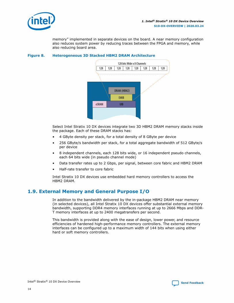
Figure 8. Heterogeneous 3D Stacked HBM2 DRAM Architecture
128 128 128 128 128 128 128 128128 bits Wide x 8 Channels
DRAM (HBM2)
EMIB
UIBeSRAM
Select Intel Stratix 10 DX devices integrate two 3D HBM2 DRAM memory stacks insidethe package. Each of these DRAM stacks has:
• 4 GByte density per stack, for a total density of 8 GByte per device
• 256 GByte/s bandwidth per stack, for a total aggregate bandwidth of 512 GByte/sper device
• 8 independent channels, each 128 bits wide, or 16 independent pseudo channels,each 64 bits wide (in pseudo channel mode)
• Data transfer rates up to 2 Gbps, per signal, between core fabric and HBM2 DRAM
• Half-rate transfer to core fabric
Intel Stratix 10 DX devices use embedded hard memory controllers to access theHBM2 DRAM.
1.9. External Memory and General Purpose I/O
In addition to the bandwidth delivered by the in-package HBM2 DRAM near memory(in selected devices), all Intel Stratix 10 DX devices offer substantial external memorybandwidth, supporting DDR4 memory interfaces running at up to 2666 Mbps and DDR-T memory interfaces at up to 2400 megatransfers per second.
This bandwidth is provided along with the ease of design, lower power, and resourceefficiencies of hardened high-performance memory controllers. The external memoryinterfaces can be configured up to a maximum width of 144 bits when using eitherhard or soft memory controllers.
1. Intel® Stratix® 10 DX Device Overview
S10-DX-OVERVIEW | 2020.03.24
Intel® Stratix® 10 DX Device Overview Send Feedback
14
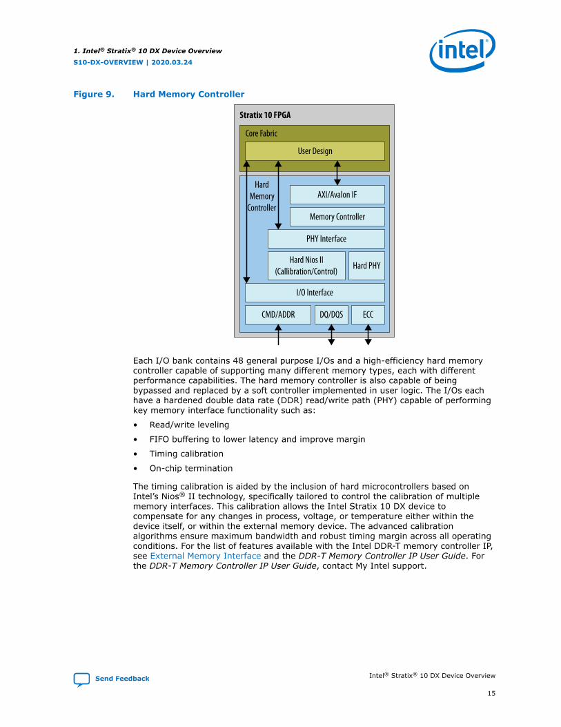
Figure 9. Hard Memory Controller
AXI/Avalon IF
Memory Controller
PHY Interface
Hard PHYHard Nios II
(Callibration/Control)
I/O Interface
ECCDQ/DQSCMD/ADDR
User Design
Core Fabric
Stratix 10 FPGA
HardMemory
Controller
Each I/O bank contains 48 general purpose I/Os and a high-efficiency hard memorycontroller capable of supporting many different memory types, each with differentperformance capabilities. The hard memory controller is also capable of beingbypassed and replaced by a soft controller implemented in user logic. The I/Os eachhave a hardened double data rate (DDR) read/write path (PHY) capable of performingkey memory interface functionality such as:
• Read/write leveling
• FIFO buffering to lower latency and improve margin
• Timing calibration
• On-chip termination
The timing calibration is aided by the inclusion of hard microcontrollers based onIntel’s Nios® II technology, specifically tailored to control the calibration of multiplememory interfaces. This calibration allows the Intel Stratix 10 DX device tocompensate for any changes in process, voltage, or temperature either within thedevice itself, or within the external memory device. The advanced calibrationalgorithms ensure maximum bandwidth and robust timing margin across all operatingconditions. For the list of features available with the Intel DDR-T memory controller IP,see External Memory Interface and the DDR-T Memory Controller IP User Guide. Forthe DDR-T Memory Controller IP User Guide, contact My Intel support.
1. Intel® Stratix® 10 DX Device Overview
S10-DX-OVERVIEW | 2020.03.24
Send Feedback Intel® Stratix® 10 DX Device Overview
15
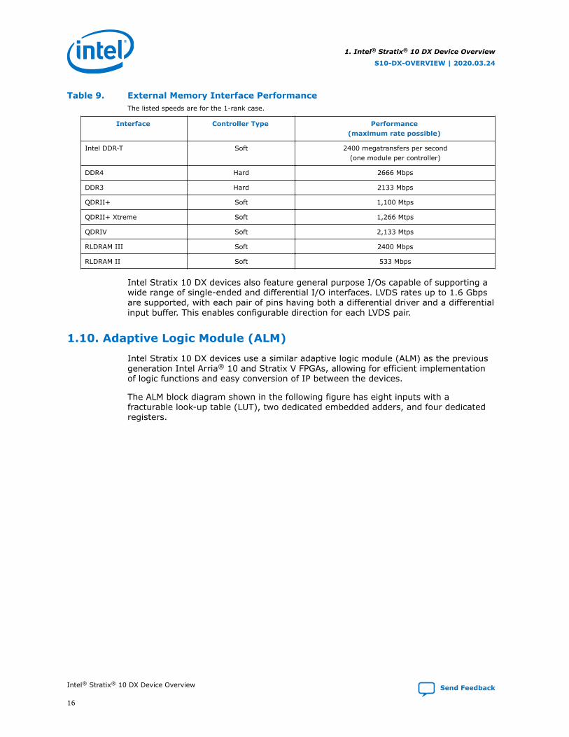
Table 9. External Memory Interface PerformanceThe listed speeds are for the 1-rank case.
Interface Controller Type Performance(maximum rate possible)
Intel DDR-T Soft 2400 megatransfers per second(one module per controller)
DDR4 Hard 2666 Mbps
DDR3 Hard 2133 Mbps
QDRII+ Soft 1,100 Mtps
QDRII+ Xtreme Soft 1,266 Mtps
QDRIV Soft 2,133 Mtps
RLDRAM III Soft 2400 Mbps
RLDRAM II Soft 533 Mbps
Intel Stratix 10 DX devices also feature general purpose I/Os capable of supporting awide range of single-ended and differential I/O interfaces. LVDS rates up to 1.6 Gbpsare supported, with each pair of pins having both a differential driver and a differentialinput buffer. This enables configurable direction for each LVDS pair.
1.10. Adaptive Logic Module (ALM)
Intel Stratix 10 DX devices use a similar adaptive logic module (ALM) as the previousgeneration Intel Arria® 10 and Stratix V FPGAs, allowing for efficient implementationof logic functions and easy conversion of IP between the devices.
The ALM block diagram shown in the following figure has eight inputs with afracturable look-up table (LUT), two dedicated embedded adders, and four dedicatedregisters.
1. Intel® Stratix® 10 DX Device Overview
S10-DX-OVERVIEW | 2020.03.24
Intel® Stratix® 10 DX Device Overview Send Feedback
16
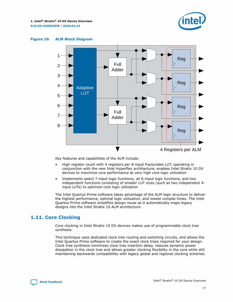
Figure 10. ALM Block Diagram
Reg
Reg
1
2
3
4
5
6
7
8
Reg
Reg
4 Registers per ALM
FullAdder
FullAdder
AdaptiveLUT
Key features and capabilities of the ALM include:
• High register count with 4 registers per 8-input fracturable LUT, operating inconjunction with the new Intel Hyperflex architecture, enables Intel Stratix 10 DXdevices to maximize core performance at very high core logic utilization
• Implements select 7-input logic functions, all 6-input logic functions, and twoindependent functions consisting of smaller LUT sizes (such as two independent 4-input LUTs) to optimize core logic utilization
The Intel Quartus Prime software takes advantage of the ALM logic structure to deliverthe highest performance, optimal logic utilization, and lowest compile times. The IntelQuartus Prime software simplifies design reuse as it automatically maps legacydesigns into the Intel Stratix 10 ALM architecture.
1.11. Core Clocking
Core clocking in Intel Stratix 10 DX devices makes use of programmable clock treesynthesis.
This technique uses dedicated clock tree routing and switching circuits, and allows theIntel Quartus Prime software to create the exact clock trees required for your design.Clock tree synthesis minimizes clock tree insertion delay, reduces dynamic powerdissipation in the clock tree and allows greater clocking flexibility in the core while stillmaintaining backwards compatibility with legacy global and regional clocking schemes.
1. Intel® Stratix® 10 DX Device Overview
S10-DX-OVERVIEW | 2020.03.24
Send Feedback Intel® Stratix® 10 DX Device Overview
17
The core clock network in Intel Stratix 10 DX devices supports the high-performanceIntel Hyperflex core architecture and also supports the hard memory controllers atrates up to 2666 Mbps with a quarter rate transfer to the core. The core clock networkis driven by either dedicated clock input pins, or integer I/O PLLs.
1.12. I/O PLLs
Intel Stratix 10 DX devices contain up to 24 integer I/O PLLs (IOPLLs) available forgeneral purpose use in the core fabric and for simplifying the design of externalmemory interfaces and high-speed LVDS interfaces. The IOPLLs are located in eachbank of 48 general purpose I/O, one per I/O bank, adjacent to the hard memorycontrollers and LVDS SerDes in each I/O bank. This makes it easier to close timingbecause the IOPLLs are tightly coupled with I/Os that need to use them. The IOPLLscan be used for general purpose applications in the core such as clock network delaycompensation and zero-delay clock buffering
1.13. Internal Embedded Memory
Intel Stratix 10 DX devices contain three types of embedded memory blocks: eSRAM(47.25 Mbit), M20K (20 Kb), and MLAB (640 bit). This variety of on-chip memoryprovides fast access times and low latency for applications such as wide and deepFIFOs and variable buffers. Combined with the in-package memory provided by theHBM2 DRAM stacks in select devices, the internal embedded memory completes thememory hierarchy in Intel Stratix 10 DX devices.
The eSRAM blocks are a new innovation in Intel Stratix 10 devices. These largeembedded SRAM blocks are tightly coupled to the core fabric and are directlyaccessible with no need for a separate memory controller. Each eSRAM block isarranged as 8 channels, 42 banks per channel, with a total capacity of 47.25 Mbitsrunning at clock rates up to 750 MHz. Within the eSRAM block, each channel has a buswidth of 72 bit read and 72 bit write, and has one READ and one WRITE per channel.This allows each eSRAM block to support a total aggregate bandwidth (read + write)of up to 864 Gbps.
The eSRAM block is implemented as a simple dual port memory with concurrent readand write access per channel, and includes integrated hard ECC generation andchecking. Compared to an off-chip SRAM solution, the eSRAM block allows you toreduce system power and save board space and cost.
The M20K and MLAB blocks are familiar block sizes carried over from previous Inteldevice families. The MLAB blocks are ideal for wide and shallow memories, while theM20K blocks are intended to support larger memory configurations and include hardECC. Both M20K and MLAB embedded memory blocks can be configured as a single-port or dual-port RAM, FIFO, ROM, or shift register. These memory blocks are highlyflexible and support a number of memory configurations as shown in the table.
Table 10. Internal Embedded Memory Block Configurations
MLAB (640 bits) M20K (20 Kb)
64 x 10 (supported through emulation)32 x 20
2K x 10 (or x8)1K x 20 (or x16)512 x 40 (or x32)
1. Intel® Stratix® 10 DX Device Overview
S10-DX-OVERVIEW | 2020.03.24
Intel® Stratix® 10 DX Device Overview Send Feedback
18
1.14. Variable Precision DSP Block
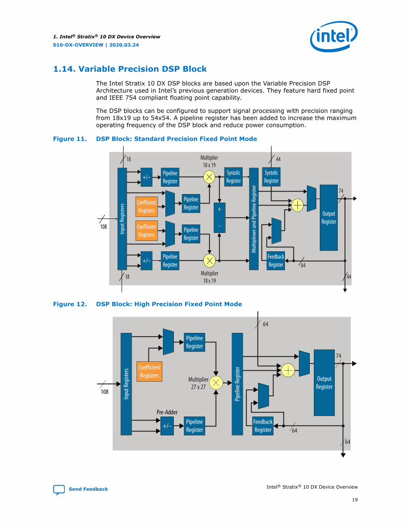
The Intel Stratix 10 DX DSP blocks are based upon the Variable Precision DSPArchitecture used in Intel’s previous generation devices. They feature hard fixed pointand IEEE 754 compliant floating point capability.
The DSP blocks can be configured to support signal processing with precision rangingfrom 18x19 up to 54x54. A pipeline register has been added to increase the maximumoperating frequency of the DSP block and reduce power consumption.
Figure 11. DSP Block: Standard Precision Fixed Point Mode
Multiplier18 x 19
4418
Inpu
t Reg
ister
s
+/–
+/–
CoefficientRegisters
CoefficientRegisters
PipelineRegister
PipelineRegister
PipelineRegister
PipelineRegister
Multiplier18 x 19
+
–
SystolicRegister
SystolicRegister
Mul
tiple
xer a
nd P
ipel
ine
Regi
ster
FeedbackRegister
OutputRegister
44
64
74
18
108
Figure 12. DSP Block: High Precision Fixed Point Mode
64
Inpu
t Reg
ister
s
+/–
CoefficientRegisters
PipelineRegister
PipelineRegister
Multiplier27 x 27
Pipeli
ne Re
giste
r
FeedbackRegister
OutputRegister
64
64
74
108
Pre-Adder
1. Intel® Stratix® 10 DX Device Overview
S10-DX-OVERVIEW | 2020.03.24
Send Feedback Intel® Stratix® 10 DX Device Overview
19
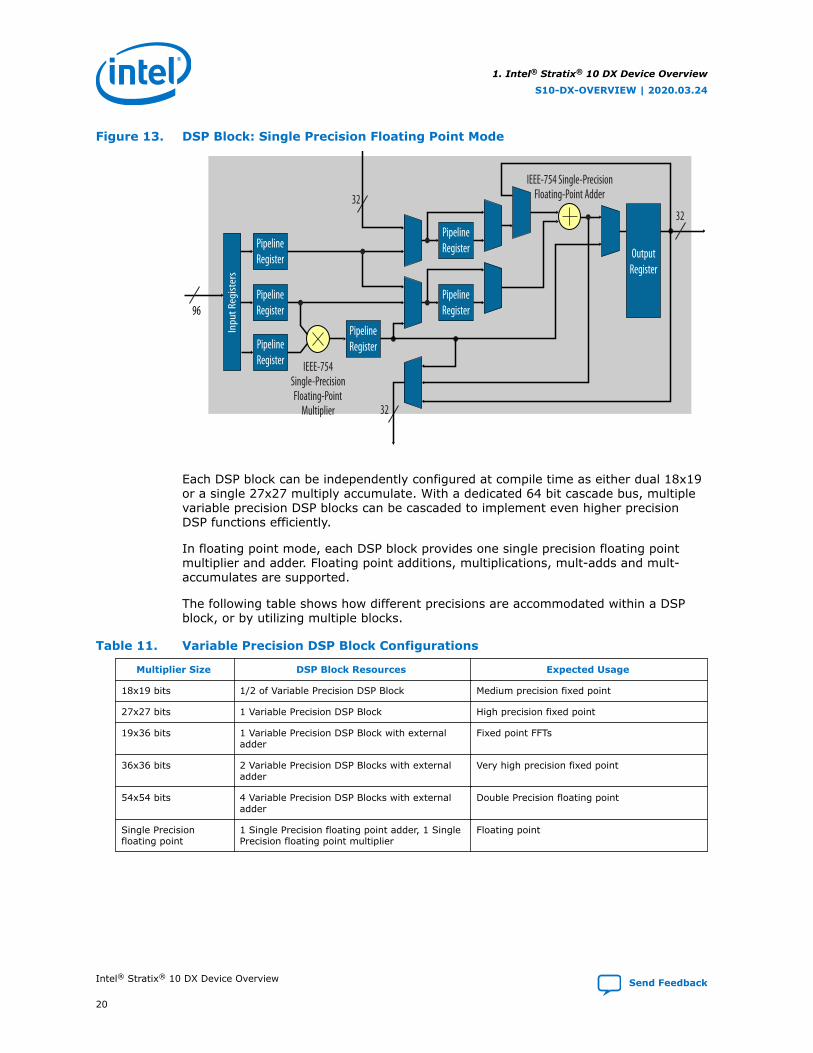
Figure 13. DSP Block: Single Precision Floating Point Mode
32
Inpu
t Reg
ister
sPipelineRegister
PipelineRegister IEEE-754
Single-PrecisionFloating-Point
Multiplier
OutputRegister
3232
96PipelineRegister
PipelineRegister
PipelineRegister
PipelineRegister
IEEE-754 Single-PrecisionFloating-Point Adder
Each DSP block can be independently configured at compile time as either dual 18x19or a single 27x27 multiply accumulate. With a dedicated 64 bit cascade bus, multiplevariable precision DSP blocks can be cascaded to implement even higher precisionDSP functions efficiently.
In floating point mode, each DSP block provides one single precision floating pointmultiplier and adder. Floating point additions, multiplications, mult-adds and mult-accumulates are supported.
The following table shows how different precisions are accommodated within a DSPblock, or by utilizing multiple blocks.
Table 11. Variable Precision DSP Block Configurations
Multiplier Size DSP Block Resources Expected Usage
18x19 bits 1/2 of Variable Precision DSP Block Medium precision fixed point
27x27 bits 1 Variable Precision DSP Block High precision fixed point
19x36 bits 1 Variable Precision DSP Block with externaladder
Fixed point FFTs
36x36 bits 2 Variable Precision DSP Blocks with externaladder
Very high precision fixed point
54x54 bits 4 Variable Precision DSP Blocks with externaladder
Double Precision floating point
Single Precisionfloating point
1 Single Precision floating point adder, 1 SinglePrecision floating point multiplier
Floating point
1. Intel® Stratix® 10 DX Device Overview
S10-DX-OVERVIEW | 2020.03.24
Intel® Stratix® 10 DX Device Overview Send Feedback
20
Complex multiplication is very common in DSP algorithms. One of the most popularapplications of complex multipliers is the FFT algorithm. This algorithm has thecharacteristic of increasing precision requirements on only one side of the multiplier.The Variable Precision DSP block supports the FFT algorithm with proportional increasein DSP resources as the precision grows.
Table 12. Complex Multiplication With Variable Precision DSP Block
Complex MultiplierSize
DSP Block Resources FFT Usage
18x19 bits 2 Variable Precision DSP Blocks Resource optimized FFT
27x27 bits 4 Variable Precision DSP Blocks Highest precision FFT
For FFT applications with high dynamic range requirements, the Intel FFT IP Coreoffers an option of single precision floating point implementation with resource usageand performance similar to high precision fixed point implementations.
Other features of the DSP block include:
• Hard 18 bit and 25 bit pre-adders
• Hard floating point multipliers and adders
• 64 bit dual accumulator (for separate I, Q product accumulations)
• Cascaded output adder chains for 18 and 27 bit FIR filters
• Embedded coefficient registers for 18 and 27 bit coefficients
• Fully independent multiplier outputs
• Inferability using HDL templates supplied by the Intel Quartus Prime software formost modes
The Variable Precision DSP block is ideal to support the growing trend towards higherbit precision in high performance DSP applications. At the same time, it can efficientlysupport the many existing 18 bit DSP applications, such as high definition videoprocessing and remote radio heads. With the Variable Precision DSP block architectureand hard floating point multipliers and adders, Intel Stratix 10 DX devices canefficiently support many different precision levels up to and including floating pointimplementations. This flexibility can result in increased system performance, reducedpower consumption, and reduce architecture constraints on system algorithmdesigners.
1.15. Hard Processor System (HPS)
The Hard Processor System (HPS) in select Intel Stratix 10 DX devices is Intel's thirdgeneration HPS. Leveraging the performance of Intel 14 nm tri-gate technology, theHPS provides more than double the performance of previous generation devices withan integrated quad-core 64-bit Arm Cortex-A53. The HPS also enables system-widehardware virtualization capabilities by adding a system memory management unit.
1. Intel® Stratix® 10 DX Device Overview
S10-DX-OVERVIEW | 2020.03.24
Send Feedback Intel® Stratix® 10 DX Device Overview
21
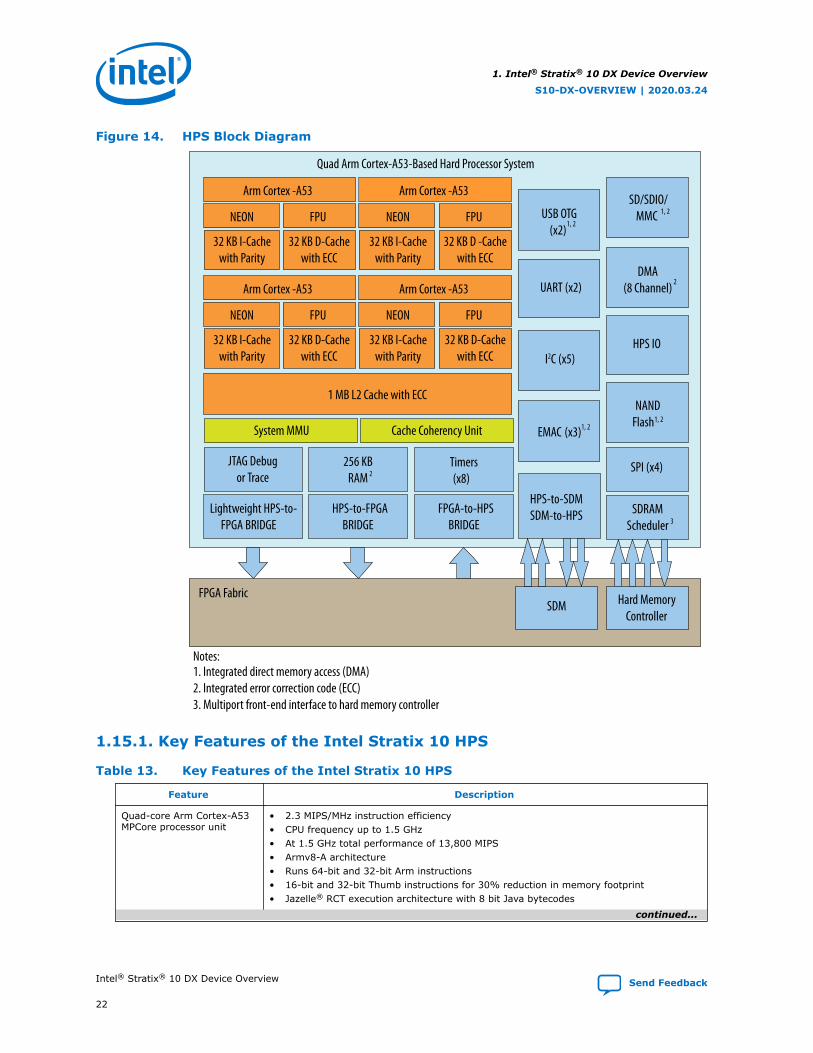
Figure 14. HPS Block Diagram
Quad Arm Cortex-A53-Based Hard Processor System
1 MB L2 Cache with ECC
JTAG Debugor Trace
256 KBRAM
Timers(x8)
HPS-to-FPGABRIDGE
FPGA-to-HPSBRIDGE
SD/SDIO/MMCUSB OTG
(x2)
DMA(8 Channel)UART (x2)
HPS IOI2C (x5)
NANDFlash1, 2
EMAC (x3)
SPI (x4)
SDRAMScheduler 3
HPS-to-SDMSDM-to-HPS
Notes:1. Integrated direct memory access (DMA)2. Integrated error correction code (ECC)3. Multiport front-end interface to hard memory controller
System MMU Cache Coherency Unit
Arm Cortex -A53
NEON FPU
32 KB I-Cachewith Parity
32 KB D-Cachewith ECC
Arm Cortex -A53
NEON FPU
32 KB I-Cachewith Parity
32 KB D -Cachewith ECC
Arm Cortex -A53
NEON FPU
32 KB I-Cachewith Parity
32 KB D-Cachewith ECC
Arm Cortex -A53
NEON FPU
32 KB I-Cachewith Parity
32 KB D-Cachewith ECC
SDM Hard MemoryController
FPGA Fabric
Lightweight HPS-to-FPGA BRIDGE
2
1, 2
1, 2
2
1, 2
1.15.1. Key Features of the Intel Stratix 10 HPS
Table 13. Key Features of the Intel Stratix 10 HPS
Feature Description
Quad-core Arm Cortex-A53MPCore processor unit
• 2.3 MIPS/MHz instruction efficiency• CPU frequency up to 1.5 GHz• At 1.5 GHz total performance of 13,800 MIPS• Armv8-A architecture• Runs 64-bit and 32-bit Arm instructions• 16-bit and 32-bit Thumb instructions for 30% reduction in memory footprint• Jazelle® RCT execution architecture with 8 bit Java bytecodes
continued...
1. Intel® Stratix® 10 DX Device Overview
S10-DX-OVERVIEW | 2020.03.24
Intel® Stratix® 10 DX Device Overview Send Feedback
22
Feature Description
• Superscalar, variable length, out-of-order pipeline with dynamic branch prediction• Improved Arm NEON™ media processing engine• Single- and double-precision floating-point unit• CoreSight™ debug and trace technology
System MemoryManagement Unit
• Enables a unified memory model and extends hardware virtualization into peripheralsimplemented in the FPGA fabric
Cache Coherency unit • Changes in shared data stored in cache are propagated throughout the systemproviding bi-directional coherency for co-processing elements.
Cache • L1 Cache— 32 KB of instruction cache w/ parity check— 32 KB of L1 data cache w /ECC— Parity checking
• L2 Cache— 1MB shared— 8-way set associative— SEU Protection with parity on TAG ram and ECC on data RAM— Cache lockdown support
On-Chip Memory • 256 KB of scratch on-chip RAM
External SDRAM and FlashMemory Interfaces for HPS
• Hard memory controller with support for DDR4, DDR3— 40 bit (32 bit + 8 bit ECC) with select packages supporting 72 bit (64 bit + 8 bit
ECC)— Support for up to 2666 Mbps DDR4 and 2166 Mbps DDR3 frequencies— Error correction code (ECC) support including calculation, error correction, write-
back correction, and error counters— Software Configurable Priority Scheduling on individual SDRAM bursts— Fully programmable timing parameter support for all JEDEC-specified timing
parameters— Multiport front-end (MPFE) scheduler interface to the hard memory controller, which
supports the AXI® Quality of Service (QoS) for interface to the FPGA fabric• NAND flash controller
— ONFI 1.0— Integrated descriptor based with DMA— Programmable hardware ECC support— Support for 8 and 16 bit Flash devices
• Secure Digital SD/SDIO/MMC controller— eMMC 4.5— Integrated descriptor based DMA— CE-ATA digital commands supported— 50 MHz operating frequency
• Direct memory access (DMA) controller— 8-channel— Supports up to 32 peripheral handshake interface
continued...
1. Intel® Stratix® 10 DX Device Overview
S10-DX-OVERVIEW | 2020.03.24
Send Feedback Intel® Stratix® 10 DX Device Overview
23
Feature Description
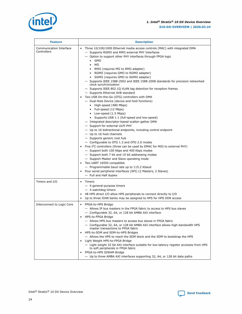
Communication InterfaceControllers
• Three 10/100/1000 Ethernet media access controls (MAC) with integrated DMA— Supports RGMII and RMII external PHY Interfaces— Option to support other PHY interfaces through FPGA logic
• GMII• MII• RMII (requires MII to RMII adapter)• RGMII (requires GMII to RGMII adapter)• SGMII (requires GMII to SGMII adapter)
— Supports IEEE 1588-2002 and IEEE 1588-2008 standards for precision networkedclock synchronization
— Supports IEEE 802.1Q VLAN tag detection for reception frames— Supports Ethernet AVB standard
• Two USB On-the-Go (OTG) controllers with DMA— Dual-Role Device (device and host functions)
• High-speed (480 Mbps)• Full-speed (12 Mbps)• Low-speed (1.5 Mbps)• Supports USB 1.1 (full-speed and low-speed)
— Integrated descriptor-based scatter-gather DMA— Support for external ULPI PHY— Up to 16 bidirectional endpoints, including control endpoint— Up to 16 host channels— Supports generic root hub— Configurable to OTG 1.3 and OTG 2.0 modes
• Five I2C controllers (three can be used by EMAC for MIO to external PHY)— Support both 100 Kbps and 400 Kbps modes— Support both 7 bit and 10 bit addressing modes— Support Master and Slave operating mode
• Two UART 16550 compatible— Programmable baud rate up to 115.2 Kbaud
• Four serial peripheral interfaces (SPI) (2 Masters, 2 Slaves)— Full and Half duplex
Timers and I/O • Timers— 4 general-purpose timers— 4 watchdog timers
• 48 HPS direct I/O allow HPS peripherals to connect directly to I/O• Up to three IO48 banks may be assigned to HPS for HPS DDR access
Interconnect to Logic Core • FPGA-to-HPS Bridge— Allows IP bus masters in the FPGA fabric to access to HPS bus slaves— Configurable 32, 64, or 128 bit AMBA AXI interface
• HPS-to-FPGA Bridge— Allows HPS bus masters to access bus slaves in FPGA fabric— Configurable 32, 64, or 128 bit AMBA AXI interface allows high-bandwidth HPS
master transactions to FPGA fabric• HPS-to-SDM and SDM-to-HPS Bridges
— Allows the HPS to reach the SDM block and the SDM to bootstrap the HPS• Light Weight HPS-to-FPGA Bridge
— Light weight 32 bit AXI interface suitable for low-latency register accesses from HPSto soft peripherals in FPGA fabric
• FPGA-to-HPS SDRAM Bridge— Up to three AMBA AXI interfaces supporting 32, 64, or 128 bit data paths
1. Intel® Stratix® 10 DX Device Overview
S10-DX-OVERVIEW | 2020.03.24
Intel® Stratix® 10 DX Device Overview Send Feedback
24
1.16. Power Management
Intel Stratix 10 DX devices use the advanced Intel 14 nm tri-gate process technology,the all new Intel Hyperflex core architecture to enable Hyper-Folding, power gating,and optional power reduction techniques to reduce total power consumption by asmuch as 70% compared to previous generation high-performance Stratix V devices.
Intel Stratix 10 standard power devices (-V) are SmartVID devices. The core voltagesupplies (VCC and VCCP) for each SmartVID device must be driven by a PMBusvoltage regulator dedicated to that Intel Stratix 10 device. Use of a PMBus voltageregulator for each SmartVID (-V) device is mandatory; it is not an option. A code isprogrammed into each SmartVID device during manufacturing that allows the PMBusvoltage regulator to operate at the optimum core voltage to meet the deviceperformance specifications.
With the new Intel Hyperflex core architecture, designs can run faster than previousgeneration FPGAs. With faster performance and same required throughput, architectscan reduce the width of the data path to save power. This optimization is called Hyper-Folding. Additionally, power gating reduces static power of unused resources in theFPGA by powering them down. The Intel Quartus Prime software automatically powersdown specific unused resource blocks such as DSP and M20K blocks, at configurationtime.
Furthermore, Intel Stratix 10 DX devices feature Intel’s low power transceivers andinclude a number of hard IP blocks that not only reduce logic resources but alsodeliver substantial power savings compared to soft implementations. In general, hardIP blocks consume up to 50% less power than the equivalent soft logicimplementations.
1.17. Device Configuration and Secure Device Manager (SDM)
All Intel Stratix 10 DX devices contain a Secure Device Manager (SDM), which is adedicated triple-redundant processor that serves as the point of entry into the devicefor all JTAG and configuration commands. The SDM also bootstraps the HPS in SoCdevices ensuring that the HPS can boot using the same security features that theFPGA devices have.
1. Intel® Stratix® 10 DX Device Overview
S10-DX-OVERVIEW | 2020.03.24
Send Feedback Intel® Stratix® 10 DX Device Overview
25
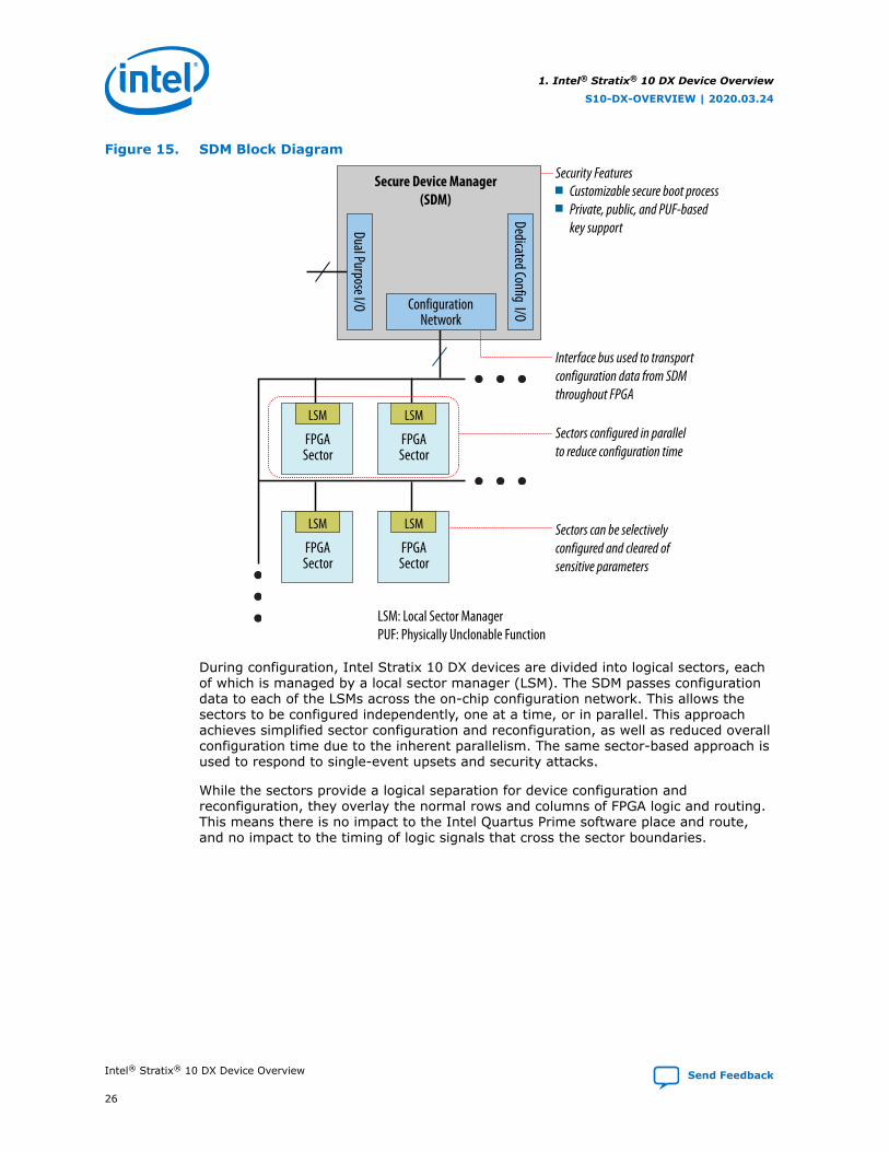
Figure 15. SDM Block Diagram
Secure Device Manager(SDM)
Dedicated Config I/O
FPGASector
LSM
FPGASector
LSM
FPGASector
LSM
FPGASector
LSMDual Purpose I/O Configuration
Network
Customizable secure boot processPrivate, public, and PUF-based key support
Security Features
Interface bus used to transport configuration data from SDM throughout FPGA
Sectors can be selectively configured and cleared of sensitive parameters
Sectors configured in parallel to reduce configuration time
LSM: Local Sector ManagerPUF: Physically Unclonable Function
During configuration, Intel Stratix 10 DX devices are divided into logical sectors, eachof which is managed by a local sector manager (LSM). The SDM passes configurationdata to each of the LSMs across the on-chip configuration network. This allows thesectors to be configured independently, one at a time, or in parallel. This approachachieves simplified sector configuration and reconfiguration, as well as reduced overallconfiguration time due to the inherent parallelism. The same sector-based approach isused to respond to single-event upsets and security attacks.
While the sectors provide a logical separation for device configuration andreconfiguration, they overlay the normal rows and columns of FPGA logic and routing.This means there is no impact to the Intel Quartus Prime software place and route,and no impact to the timing of logic signals that cross the sector boundaries.
1. Intel® Stratix® 10 DX Device Overview
S10-DX-OVERVIEW | 2020.03.24
Intel® Stratix® 10 DX Device Overview Send Feedback
26
The SDM enables robust, secure, fully-authenticated device configuration. It alsoallows for customization of the configuration scheme, which can enhance devicesecurity. For configuration and reconfiguration, this approach offers a variety ofadvantages:
• Dedicated secure configuration manager
• Reduced device configuration time, because sectors are configured in parallel
• Updateable configuration process
• Reconfiguration of one or more sectors independent of all other sectors
• Zeroization of individual sectors or the complete device
1.18. Device Security
Building on top of the robust security features present in the previous generationdevices, Intel Stratix 10 DX devices include a number of new and innovative securityenhancements. These features are also managed by the SDM, tightly coupling deviceconfiguration and reconfiguration with encryption, authentication, key storage andanti-tamper services.
Security services provided by the SDM include:
• Bitstream encryption
• Multi-factor authentication
• Hard encryption and authentication acceleration; AES-256, SHA-256/384,ECDSA-256/384
• Volatile and non-volatile encryption key storage and management
• Physically Unclonable Function (PUF) service
• Updateable configuration process
• Secure device maintenance and upgrade functions
• Side channel attack protection
• Scripted response to sensor inputs and security attacks, including selective sectorzeroization
• Readback, JTAG and test mode disable
• Enhanced response to single-event upsets (SEU)
• Black key provisioning
• Physical anti-tamper
See the Intel Stratix 10 Device Security User Guide for a complete list of all securityfeatures.
The SDM and associated security services provide a robust, multi-layered securitysolution for your Intel Stratix 10 DX design.
1. Intel® Stratix® 10 DX Device Overview
S10-DX-OVERVIEW | 2020.03.24
Send Feedback Intel® Stratix® 10 DX Device Overview
27
Table 14. Device Security
Intel Stratix 10 Family Variant Bitstream Authentication Advanced Security Features(6)
DX All devices All devices
Related Information
• My Intel Support
• Intel Stratix 10 Device Security User Guide
1.19. Configuration via Protocol Using PCI Express
Configuration via protocol using PCI Express allows the FPGA to be configured acrossthe PCI Express bus, simplifying the board layout and increasing system integration.Making use of the embedded PCI Express hard IP operating in autonomous modebefore the FPGA is configured, this technique allows the PCI Express bus to bepowered up and active within the 100 ms time allowed by the PCI Expressspecification. Intel Stratix 10 DX devices also support partial reconfiguration acrossthe PCI Express bus which reduces system down time by keeping the PCI Express linkactive while the device is being reconfigured.
1.20. Partial and Dynamic Reconfiguration
Partial reconfiguration allows you to reconfigure part of the FPGA while other sectionscontinue running. This capability is required in systems where uptime is critical,because it allows you to make updates or adjust functionality without disruptingservices.
In addition to lowering power and cost, partial reconfiguration also increases theeffective logic density by removing the necessity to place in the FPGA those functionsthat do not operate simultaneously. Instead, these functions can be stored in externalmemory and loaded as needed. This reduces the size of the required FPGA by allowingmultiple applications on a single FPGA, saving board space and reducing power. Thepartial reconfiguration process is built on top of the proven incremental compile designflow in the Intel Quartus Prime design software
Dynamic reconfiguration in Intel Stratix 10 DX devices allows transceiver data rates,protocols and analog settings to be changed dynamically on a channel-by-channelbasis while maintaining data transfer on adjacent transceiver channels. Dynamicreconfiguration is ideal for applications that require on-the-fly multiprotocol or multi-rate support. Both the PMA and PCS blocks within the transceiver can be reconfiguredusing this technique. Dynamic reconfiguration of the transceivers can be used inconjunction with partial reconfiguration of the FPGA to enable partial reconfiguration ofboth core and transceivers simultaneously.
1.21. Fast Forward Compile
The innovative Fast Forward Compile feature in the Intel Quartus Prime softwareidentifies performance bottlenecks in your design and provides detailed, step-by-stepperformance improvement recommendations that you can then implement. TheCompiler reports estimates of the maximum operating frequency that can be achieved
(6) Contact My Intel Support for additional information.
1. Intel® Stratix® 10 DX Device Overview
S10-DX-OVERVIEW | 2020.03.24
Intel® Stratix® 10 DX Device Overview Send Feedback
28
by applying the recommendations. As part of the new Hyper-Aware design flow, FastForward Compile maximizes the performance of your Intel Stratix 10 DX design andachieves rapid timing closure.
Previously, this type of optimization required multiple time-consuming designiterations, including full design re-compilation to determine the effectiveness of thechanges. Fast Forward Compile enables you to make better decisions about where tofocus your optimization efforts, and how to increase your design performance andthroughput. This technique removes much of the guesswork of performanceexploration, resulting in fewer design iterations.
1.22. Single Event Upset (SEU) Error Detection and Correction
Intel Stratix 10 DX devices offer robust SEU error detection and correction circuitry.The detection and correction circuitry includes protection for Configuration RAM(CRAM) programming bits and user memories. The CRAM is protected by acontinuously running parity checker circuit with integrated ECC that automaticallycorrects one or two bit errors and detects higher order multibit errors.
The physical layout of the CRAM array is optimized to make the majority of multi-bitupsets appear as independent single-bit or double-bit errors which are automaticallycorrected by the integrated CRAM ECC circuitry. In addition to the CRAM protection,user memories also include integrated ECC circuitry and are layout optimized for errordetection and correction.
The SEU error detection and correction hardware is supported by both soft IP and theIntel Quartus Prime software to provide a complete SEU mitigation solution. Thecomponents of the complete solution include:
• Hard error detection and correction for CRAM and user eSRAM and M20K memoryblocks
• Optimized physical layout of memory cells to minimize probability of SEU
• Sensitivity processing soft IP that reports if CRAM upset affects a used or unusedbit
• Fault injection soft IP with the Intel Quartus Prime software support that changesstate of CRAM bits for testing purposes
• Hierarchy tagging in the Intel Quartus Prime software
• Triple Mode Redundancy (TMR) used for the Secure Device Manager and criticalon-chip state machines
In addition to the SEU mitigation features listed above, the Intel 14 nm tri-gateprocess technology used for Intel Stratix 10 DX devices is based on FinFET transistorswhich have reduced SEU susceptibility versus conventional planar transistors.
1.23. Document Revision History for the Intel Stratix 10 DX DeviceOverview
Document Version Changes
2020.03.24 Made the following changes:• Added advanced security (-AS) devices.• Added Intel Optane memory support.
2019.09.19 Initial release.
1. Intel® Stratix® 10 DX Device Overview
S10-DX-OVERVIEW | 2020.03.24
Send Feedback Intel® Stratix® 10 DX Device Overview
29