Embed Size (px)
Citation preview
Intel® Stratix® 10
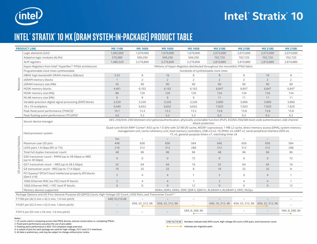
Intel® StratIx® 10 Mx (DraM SySteM-In-Package) ProDuct table
Notes:1. LE counts valid in comparing across Intel FPGA devices, and are conservative vs. competing FPGAs.2. Fixed-point performance assumes the use of pre-adder.3. Floating-point performance is IEEE 754 compliant single precision.4. A subset of pins for each package are used for high-voltage, 3.0 V and 2.5 V interfaces.5. All data is preliminary, and may be subject to change without prior notice.
PRODUCT LINE MX 1100 MX 1650 MX 1650 MX 1650 MX 2100 MX 2100 MX 2100 MX 2100
Reso
urce
s
Logic elements (LEs)1 1,092,000 1,679,000 1,679,000 1,679,000 2,073,000 2,073,000 2,073,000 2,073,000Adaptive logic modules (ALMs) 370,080 569,200 569,200 569,200 702,720 702,720 702,720 702,720ALM registers 1,480,320 2,276,800 2,276,800 2,276,800 2,810,880 2,810,880 2,810,880 2,810,880Hyper-Registers from Intel® HyperflexTM FPGA architecture Millions of Hyper-Registers distributed throughout the monolithic FPGA fabricProgrammable clock trees synthesizable Hundreds of synthesizable clock treesHBM2 high-bandwidth DRAM memory (GBytes) 3.25 8 16 8 8 8 16 8eSRAM memory blocks 1 2 2 2 2 2 2 2eSRAM memory size (Mb) 45 90 90 90 90 90 90 90M20K memory blocks 4,401 6,162 6,162 6,162 6,847 6,847 6,847 6,847M20K memory size (Mb) 86 120 120 120 134 134 134 134MLAB memory size (Mb) 6 9 9 9 11 11 11 11Variable-precision digital signal processing (DSP) blocks 2,520 3,326 3,326 3,326 3,960 3,960 3,960 3,96018 x 19 multipliers 5,040 6,652 6,652 6,652 7,920 7,920 7,920 7,920Peak fixed-point performance (TMACS)2 10.1 13.3 13.3 13.3 15.8 15.8 15.8 15.8Peak floating-point performance (TFLOPS)3 4.0 5.3 5.3 5.3 6.3 6.3 6.3 6.3
I/O a
nd A
rchi
tect
ural
Fea
ture
s
Secure device manager AES-256/SHA-256 bitstream encryption/authentication, physically unclonable function (PUF), ECDSA 256/384 boot code authentication, side channel attack protection
Hard processor system
Quad-core 64 bit ARM* Cortex*-A53 up to 1.5 GHz with 32 KB I/D cache, NEON* coprocessor, 1 MB L2 cache, direct memory access (DMA), system memory management unit, cache coherency unit, hard memory controllers, USB 2.0 x2, 1G EMAC x3, UART x2, serial peripheral interface (SPI) x4,
I2C x5, general-purpose timers x7, watchdog timer x4Yes – – – – – – –
Maximum user I/O pins 448 656 656 584 640 656 656 584LVDS pairs 1.6 Gbps (RX or TX) 216 312 312 288 312 312 312 288Total full duplex transceiver count 48 96 96 96 48 96 96 96GXE transceiver count - PAM4 (up to 58 Gbps) or NRZ (up to 30 Gbps) 0 0 0 72 0 0 0 72
GXT transceiver count - NRZ (up to 28.3 Gbps) 32 64 64 16 32 64 64 16GX transceiver count - NRZ (up to 17.4 Gbps) 16 32 32 8 16 32 32 8PCI Express* (PCIe*) hard intellectual property (IP) blocks (Gen3 x16) 2 4 4 1 2 4 4 1
100G Ethernet MAC (no FEC) hard IP blocks 2 4 4 1 2 4 4 1100G Ethernet MAC + FEC hard IP blocks 0 0 0 12 0 0 0 12Memory devices supported DDR4, DDR3, DDR2, DDR, QDR II, QDR II+, RLDRAM II, RLDRAM 3, HMC, MoSys
Package Options and I/O Pins: General-Purpose I/O (GPIO) Count, High-Voltage I/O Count, LVDS Pairs, and Transceiver Count4, 5
F1760 pin (42.5 mm x 42.5 mm, 1.0 mm pitch) 448,16,216,48 – – – – – – –
F2597 pin (52.5 mm x 52.5 mm, 1.0mm pitch) – 656, 32, 312, 96 656, 32, 312, 96 – 640, 16, 312, 48 656, 32, 312, 96 656, 32, 312, 96 –
F2912 pin (55 mm x 55 mm, 1.0 mm pitch) – – – 584, 8, 288, 96 – – – 584, 8, 288, 96
448,16,216,48 Numbers indicate total GPIO count, high-voltage I/O count, LVDS pairs, and transceiver count.
Indicates pin migration path.
© Intel Corporation. Intel, the Intel logo, the Intel Inside mark and logo, the Intel. Experience What’s Inside mark and logo, Altera, Arria, Cyclone, Enpirion, Intel Atom, Intel Core, Intel Xeon, MAX, Nios, Quartus and Stratix are trademarks of Intel Corporation or its subsidiaries in the U.S. and/or other countries. See Trademarks on intel.com for full list of Intel trademarks. *Other marks and brands may be claimed as the property of others.
StratIx 10 ProDuct table
Intel® Stratix® 10
Gen-1032-1.4
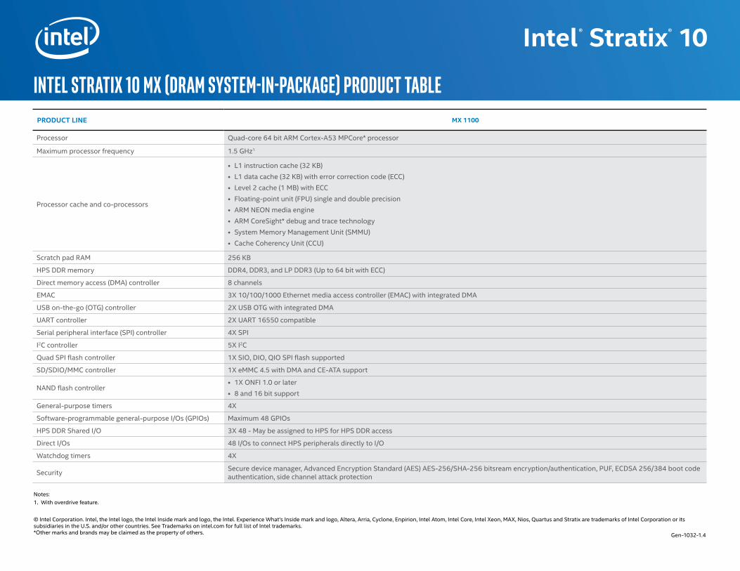
PRODUCT LINE MX 1100
Processor Quad-core 64 bit ARM Cortex-A53 MPCore* processor
Maximum processor frequency 1.5 GHz1
Processor cache and co-processors
• L1 instruction cache (32 KB) • L1 data cache (32 KB) with error correction code (ECC)• Level 2 cache (1 MB) with ECC• Floating-point unit (FPU) single and double precision• ARM NEON media engine• ARM CoreSight* debug and trace technology• System Memory Management Unit (SMMU)• Cache Coherency Unit (CCU)
Scratch pad RAM 256 KB
HPS DDR memory DDR4, DDR3, and LP DDR3 (Up to 64 bit with ECC)
Direct memory access (DMA) controller 8 channels
EMAC 3X 10/100/1000 Ethernet media access controller (EMAC) with integrated DMA
USB on-the-go (OTG) controller 2X USB OTG with integrated DMA
UART controller 2X UART 16550 compatible
Serial peripheral interface (SPI) controller 4X SPI
I2C controller 5X I2C
Quad SPI flash controller 1X SIO, DIO, QIO SPI flash supported
SD/SDIO/MMC controller 1X eMMC 4.5 with DMA and CE-ATA support
NAND flash controller• 1X ONFI 1.0 or later• 8 and 16 bit support
General-purpose timers 4X
Software-programmable general-purpose I/Os (GPIOs) Maximum 48 GPIOs
HPS DDR Shared I/O 3X 48 - May be assigned to HPS for HPS DDR access
Direct I/Os 48 I/Os to connect HPS peripherals directly to I/O
Watchdog timers 4X
Security Secure device manager, Advanced Encryption Standard (AES) AES-256/SHA-256 bitsream encryption/authentication, PUF, ECDSA 256/384 boot code authentication, side channel attack protection
Notes:1. With overdrive feature.
Intel StratIx 10 Mx (DraM SySteM-In-Package) ProDuct table