Embed Size (px)
Citation preview

Intel® High Level Synthesis CompilerUser Guide
Updated for Intel® Quartus® Prime Design Suite: 19.3
SubscribeSend Feedback
UG-20037 | 2019.09.30Latest document on the web: PDF | HTML

Contents
1. Intel® High Level Synthesis Compiler User Guide............................................................4
2. Overview of the Intel High Level Synthesis (HLS) Compiler............................................52.1. High Level Synthesis Design Flow............................................................................ 52.2. The Project Directory............................................................................................. 7
3. Creating a High-Level Synthesis Component and Testbench........................................... 83.1. Compiler-Defined Preprocessor Macros..................................................................... 9
4. Verifying the Functionality of Your Design.................................................................... 10
5. Optimizing and Refining Your Component.....................................................................11
6. Verifying Your IP with Simulation.................................................................................126.1. Generation of the Verification Testbench Executable..................................................126.2. Debugging during Verification................................................................................136.3. High-Throughput Simulation (Asynchronous Component Calls) Using Enqueue
Function Calls...................................................................................................136.3.1. Execution Model.......................................................................................146.3.2. Comparison of Explicit and Enqueued Function Calls..................................... 14
7. Synthesize your Component IP with Intel Quartus Prime............................................. 16
8. Integrating your IP into a System.................................................................................178.1. Adding the HLS Compiler-Generated IP into an Intel Quartus Prime Project..................178.2. Adding the HLS Compiler-Generated IP into a Platform Designer System..................... 18
9. Document Revision History for Intel HLS Compiler User Guide..................................... 19
A. Limitations of the Intel HLS Compiler........................................................................... 23
B. Reviewing the High Level Design Report (report.html) ............................................. 25B.1. High Level Design Report Layout............................................................................25B.2. Reviewing the Report Summary.............................................................................28B.3. Reviewing Factors That Affect Throughput...............................................................30
B.3.1. Reviewing Loop Information...................................................................... 31
B.3.2. Reviewing fmax II Information........................................................... 33B.4. Reviewing Component Area Usage......................................................................... 34
B.4.1. Area Analysis Example..............................................................................37
B.5. Viewing Component Design.......................................................................... 39
B.5.1. Graph Viewer (Beta)........................................................................41B.5.2. Function Memory Viewer...........................................................................64
B.5.3. Schedule Viewer (Alpha).................................................................. 69
B.6. Viewing Component Design.......................................................................... 70B.6.1. Reviewing Component Interfaces............................................................... 71
B.6.2. Reviewing Memory Replication and Stallable LSU Information................81
B.6.3. Viewing Your Component Memory System ......................................... 84
Contents
Intel High Level Synthesis Compiler: User Guide Send Feedback
2

B.7. Reviewing Your Component Verification Results........................................................86B.8. Accessing HLD FPGA Reports in JSON Format.......................................................... 87
Contents
Send Feedback Intel High Level Synthesis Compiler: User Guide
3

1. Intel® High Level Synthesis Compiler User GuideThe Intel® High Level Synthesis Compiler User Guide provides instructions onsynthesizing, verifying, and simulating IP that you design for Intel FPGA products. TheIntel High Level Synthesis (HLS) Compiler is sometimes referred to as the i++compiler, reflecting the name of the compiler command.
Compared to traditional RTL development, the Intel HLS Compiler offers the followingadvantages:
• Fast and easy verification
• Algorithmic development in C++
• Automatic integration of RTL verification with a C++ testbench
• Powerful microarchitecture optimizations
The features and devices supported by the Intel HLS Compiler depend on what editionof Intel Quartus® Prime you have. The following icons indicate content in thispublication that applies only to the Intel HLS Compiler provided with a certain editionof Intel Quartus Prime:
Indicates that a feature or content applies only to Intel HLS Compiler ProEdition.
Indicates that a feature or content applies only to Intel HLS CompilerStandard Edition.
In this publication, <quartus_installdir> refers to the location where youinstalled Intel Quartus Prime Design Suite.
The default Intel Quartus Prime Design Suite installation location depends on youroperating system and your Intel Quartus Prime edition:
Windows C:\intelFPGA_pro\19.3
Linux /home/<username>/intelFPGA_pro/19.3
Windows C:\intelFPGA_standard\19.3
Linux /home/<username>/intelFPGA_standard/19.3
UG-20037 | 2019.09.30
Send Feedback
Intel Corporation. All rights reserved. Agilex, Altera, Arria, Cyclone, Enpirion, Intel, the Intel logo, MAX, Nios,Quartus and Stratix words and logos are trademarks of Intel Corporation or its subsidiaries in the U.S. and/orother countries. Intel warrants performance of its FPGA and semiconductor products to current specifications inaccordance with Intel's standard warranty, but reserves the right to make changes to any products and servicesat any time without notice. Intel assumes no responsibility or liability arising out of the application or use of anyinformation, product, or service described herein except as expressly agreed to in writing by Intel. Intelcustomers are advised to obtain the latest version of device specifications before relying on any publishedinformation and before placing orders for products or services.*Other names and brands may be claimed as the property of others.
ISO9001:2015Registered

2. Overview of the Intel High Level Synthesis (HLS)Compiler
The Intel High Level Synthesis (HLS) Compiler parses your design, compiles it to anx86-64 object or FPGA-targeted RTL code, and creates an executable testbench.
The Intel HLS Compiler is command-line compatible with g++, and supports most ofthe g++ compiler flags. See the Intel High Level Synthesis Compiler Reference Manualfor a full list of compiler flags.
The Intel HLS Compiler recognizes the same file name extensions as g++,namely .c, .C, .cc, .cpp, .CPP, .c++, .cp, and .cxx. The compiler treats all ofthese file types as C++. The compiler does not explicitly support C, other than as asubset of C++.
Important: The Intel HLS Compiler Pro Edition treats all input files as C++14. The compiler
does not support files conforming to newer C++ standards.
The Intel HLS Compiler Standard Edition treats all input files as C++98. Thecompiler does not support files conforming to newer C++ standards.
When you target the compilation to an FPGA, the Intel HLS Compiler outputs anexecutable and a project directory. The default executable is a.out on Linux anda.exe on Windows. The default project directory is a.prj, and it contains HLSresults, including the generated IP. It also contains reports and auxiliary informationfor verification purposes.
To specify the name of the compiler output, include the -o <result> option in youri++ command, where <result> is the name of the executable. This commandcreates a project directory called <result>.prj.
Running the executable file runs your testbench. When you target the compilation toan x86-64 architecture, the output executable runs your design on the CPU. Theoutput executable runs very quickly compared to running a simulation of yourcomponent RTL. When you target the compilation to an FPGA architecture, the outputexecutable simulates your component RTL. This simulation can take a long time torun.
2.1. High Level Synthesis Design Flow
The Intel High Level Synthesis (HLS) Compiler helps speed your IP development byletting you compile your IP component C++ code to different targets, depending onwhere you are in your IP development cycle.
The typical design flow when you use the Intel HLS Compiler consists of the followingstages:
UG-20037 | 2019.09.30
Send Feedback
Intel Corporation. All rights reserved. Agilex, Altera, Arria, Cyclone, Enpirion, Intel, the Intel logo, MAX, Nios,Quartus and Stratix words and logos are trademarks of Intel Corporation or its subsidiaries in the U.S. and/orother countries. Intel warrants performance of its FPGA and semiconductor products to current specifications inaccordance with Intel's standard warranty, but reserves the right to make changes to any products and servicesat any time without notice. Intel assumes no responsibility or liability arising out of the application or use of anyinformation, product, or service described herein except as expressly agreed to in writing by Intel. Intelcustomers are advised to obtain the latest version of device specifications before relying on any publishedinformation and before placing orders for products or services.*Other names and brands may be claimed as the property of others.
ISO9001:2015Registered

1. Creating your component and testbench.
You can write a complete C++ application that contains both your component codeand your testbench code.
For details, see Creating a High-Level Synthesis Component and Testbench onpage 8.
2. Verify the functionality of your component algorithm and testbench.
Verify the functionality by compiling your design to x86-64 executable and runningthe executable. For details, see Verifying the Functionality of Your Design on page10.
3. Optimize and refine the FPGA performance of your component.
Optimize the FPGA performance of your component by compiling your design to anFPGA target and reviewing the high-level design report to see where you canoptimize your component. This step generates RTL code for your component. Fordetails, see Optimizing and Refining Your Component on page 11.
After initial optimizations, you can see where to further refine your component bycompiling it for simulation. For details, see Verifying Your IP with Simulation onpage 12.
4. Synthesize your component with Intel Quartus Prime.
For details, see Synthesize your Component IP with Intel Quartus Prime on page16.
Synthesizing your component generates accurate quality-of-results (QoR) metricslike FPGA area utilization and fMAX.
5. Integrate your IP into a system with Intel Quartus Prime or Platform Designer(formerly Qsys).
For details, see Integrating your IP into a System on page 17.
The following flowchart shows a coarse-grained progression through the stages of atypical Intel High Level Synthesis (HLS) Compiler design flow.
2. Overview of the Intel High Level Synthesis (HLS) Compiler
UG-20037 | 2019.09.30
Intel High Level Synthesis Compiler: User Guide Send Feedback
6

Figure 1. Overview of Procedure for Synthesizing IP for Intel FPGA Products
Create component and test bench
Compile design with the following command to generate IP and a testbench executable to verify your design in simulation:
i++ -march="<FPGA_family_or_part_number>"
Compile design with g++ or i++ -march=x86-64 for functional verification
(Note: You can debug your design using GDB, even for an i++ x86-64 output)
Run a Quartus Prime compilation on the project in the <result>.prj/quartus directory to generate QoR metrics
from Quartus Prime software
Refine Algorithm
Optimize FPGA
Performance
2.2. The Project Directory
The project directory (<result>.prj) that the Intel HLS Compiler outputs has foursubdirectories.
Table 1. Subdirectories within the .prj Directory
Directory Description
components Contains a folder for each component, and all HDL and IP files that are needed to usethat component in a design.
verification Contains all the files for the verification testbench.
reports Contains reports with information that is useful for analyzing the hardwareimplementation of the synthesized components.
quartus Contains an Intel Quartus Prime project that instantiates the components. You cancompile this Intel Quartus Prime project to generate more detailed timing and areareports.
2. Overview of the Intel High Level Synthesis (HLS) Compiler
UG-20037 | 2019.09.30
Send Feedback Intel High Level Synthesis Compiler: User Guide
7
3. Creating a High-Level Synthesis Component andTestbench
The Intel HLS Compiler converts individual functions into RTL code. The componentsare part of a C++ application that acts as a testbench for your component functions,and you can test your components by calling them from your main() function andverifying that the output is correct.
While the compiler supports C++14 (Pro Edition) or C++98 (Standard Edition), youcan often achieve better component performance by using the supported subset ofC99 whenever possible. The compiler is capable of synthesizing some C++ constructs,which might be easier for you to use to create cleaner code.
For more information about the supported subset of C99 and its restrictions, see"Supported Subset for Component Synthesis" in Intel High Level Synthesis CompilerReference Manual.
The Intel HLS Compiler synthesizes all the code in the function or functions that youlabel as components, and any code that these components call, to an RTLrepresentation.
You can identify a function in your C++ application that you want to synthesize into anIP core in one of the following ways:
• Insert the component keyword in the source code before the top-level C++function to be synthesized.
• Specify the function on the command line by using the --component<component_list> option of the i++ command.
To use this option, your component must be configured with C-linkage using theextern "C" specification. For example:
extern "C" int myComponent(int a, int b)
UG-20037 | 2019.09.30
Send Feedback
Intel Corporation. All rights reserved. Agilex, Altera, Arria, Cyclone, Enpirion, Intel, the Intel logo, MAX, Nios,Quartus and Stratix words and logos are trademarks of Intel Corporation or its subsidiaries in the U.S. and/orother countries. Intel warrants performance of its FPGA and semiconductor products to current specifications inaccordance with Intel's standard warranty, but reserves the right to make changes to any products and servicesat any time without notice. Intel assumes no responsibility or liability arising out of the application or use of anyinformation, product, or service described herein except as expressly agreed to in writing by Intel. Intelcustomers are advised to obtain the latest version of device specifications before relying on any publishedinformation and before placing orders for products or services.*Other names and brands may be claimed as the property of others.
ISO9001:2015Registered

Important: Components are synthesized for all functions labeled with the component keywordand all for all components listed in the --component <component_list> option ofthe i++ command. Avoid combining these methods because you might unexpectedlysynthesize unwanted components.
If you do not want components synthesized for a function, ensure that you do nothave the component attribute specified in the function and ensure that the function isnot specified in the --component <component_list> option of the i++ command.
You can see which components were synthesized in the summary page of thehigh-level design report (<name>.prj/reports/report.html). For moreinformation about the high-level design report, see The Intel HLS Compiler High LevelDesign Report (report.html) on page 11.
You can see which components were synthesized in the Area Analysis by Sourcesection of the high-level design report (<name>.prj/reports/report.html). Formore information about the high-level design report, see The Intel HLS Compiler HighLevel Design Report (report.html) on page 11.
The HLS compiler creates an executable to run on the CPU. The compiler then sendsany calls to functions that you declared as components to simulation of thesynthesized IP core, and the simulation results are returned.
3.1. Compiler-Defined Preprocessor Macros
The Intel HLS Compiler has a built-in macros that you can use to customize your codeto create flow-dependent behaviors.
Table 2. Macro Definition for __INTELFPGA_COMPILER__
Tool Invocation __INTELFPGA_COMPILER__
g++ or cl Undefined
i++ -march=x86-64 1930
i++ -march="<FPGA_family_or_part_number>" 1930
Table 3. Macro Definition for HLS_SYNTHESIS
Tool InvocationHLS_SYNTHESIS
Testbench Code HLS Component Code
g++ or cl Undefined Undefined
i++ -march=x86-64 Undefined Undefined
i++ -march="<FPGA_family_or_part_number>" Undefined Defined
3. Creating a High-Level Synthesis Component and Testbench
UG-20037 | 2019.09.30
Send Feedback Intel High Level Synthesis Compiler: User Guide
9

4. Verifying the Functionality of Your DesignVerify the functionality of your design by compiling your component and testbench toan x86-64 executable that you can debug with a native C++ debugger.
Compiling your design to an x86-64 executable is faster than compiling yourcomponent to hardware or a hardware simulation. This faster compilation time letsyou debug and refine your component algorithms quickly before you move on to seehow your component is implemented in hardware.
You can compile your component and testbench to an x86-64 executable for functionalverification through any of the following methods:
• Use the i++ -march=x86-64 command.
• On Linux systems, use the g++ command.
• On Windows systems, use Microsoft Visual Studio.
Ensure that you set your compiler command to include debug information. The i++command generates debug information by default.
On Linux systems, you can use GDB to debug your component and testbench, even ifyou used the i++ command to compile your code for functional verification.
Using the g++ command or Microsoft Visual Studio might require additionalconfiguration to compile your Intel HLS Compiler code. For details, see CompilerInteroperability in the Intel High Level Synthesis Compiler Reference Manual.
You can automate the process by using makefile or batch script. Use the makefiles andscripts provided in the Intel HLS Compiler example designs and tutorials as guides forcreating your own makefiles or batch scripts.
UG-20037 | 2019.09.30
Send Feedback
Intel Corporation. All rights reserved. Agilex, Altera, Arria, Cyclone, Enpirion, Intel, the Intel logo, MAX, Nios,Quartus and Stratix words and logos are trademarks of Intel Corporation or its subsidiaries in the U.S. and/orother countries. Intel warrants performance of its FPGA and semiconductor products to current specifications inaccordance with Intel's standard warranty, but reserves the right to make changes to any products and servicesat any time without notice. Intel assumes no responsibility or liability arising out of the application or use of anyinformation, product, or service described herein except as expressly agreed to in writing by Intel. Intelcustomers are advised to obtain the latest version of device specifications before relying on any publishedinformation and before placing orders for products or services.*Other names and brands may be claimed as the property of others.
ISO9001:2015Registered

5. Optimizing and Refining Your ComponentAfter you have verified the functionality of your component and testbench, you cancompile your component to RTL and review the high-level design report to furtheroptimize and refine your component design. The high-level design report showsestimates of various aspects of how your component will be implemented in hardware.By compiling your component to RTL and reviewing the high-level design report, youcan see how your code changes affect your component hardware implementationwithout needing to run a simulation or a full Quartus compilation.
To compile your component to RTL without running a simulation, issue the followingcommand:
i++ -march="<FPGA_family_or_part_number>" --simulator none
You can also compile your component with a ModelSim* simulation flow by omittingthe --simulator none option. Compiling without a simulation test bench is faster,but prevents you from co-simulating your design and measure its latency andgenerate waveforms.
The Intel HLS Compiler High Level Design Report (report.html)
The high-level design report is an HTML file called report.html that you can view ina web browser. You can find the high-level design report in the <name>.prj/reports folder created when you compile your component to RTL.
Use the high-level design report to review information about your component,including the following information:
• Loop information, including unroll status, pipelining status, and initiation interval
• Component visualization including load-store units, component interfaces, loops,and local memory systems
After you run a simulation flow, the area utilization estimates also show youverification statistics such as component latency and occupancy of your componentI/O interfaces.
After you synthesize your component with Intel Quartus Prime software, the followingadditional information is available in the report:
• Maximum clock frequency
• Accurate area usage estimate
For more information about the high-level design report and how to use it to optimizeand refine your component, see Reviewing the High Level Design Report (report.html)on page 25.
For information about techniques that you can apply to optimize and refine yourcomponent, see Intel High Level Synthesis Compiler Best Practices Guide.
UG-20037 | 2019.09.30
Send Feedback
Intel Corporation. All rights reserved. Agilex, Altera, Arria, Cyclone, Enpirion, Intel, the Intel logo, MAX, Nios,Quartus and Stratix words and logos are trademarks of Intel Corporation or its subsidiaries in the U.S. and/orother countries. Intel warrants performance of its FPGA and semiconductor products to current specifications inaccordance with Intel's standard warranty, but reserves the right to make changes to any products and servicesat any time without notice. Intel assumes no responsibility or liability arising out of the application or use of anyinformation, product, or service described herein except as expressly agreed to in writing by Intel. Intelcustomers are advised to obtain the latest version of device specifications before relying on any publishedinformation and before placing orders for products or services.*Other names and brands may be claimed as the property of others.
ISO9001:2015Registered

6. Verifying Your IP with SimulationWhen compiling your component to an FPGA architecture, the Intel HLS Compiler linksyour design C++ testbench with an RTL-compiled version of your component that runsin an RTL simulator.
The Intel HLS Compiler uses Mentor Graphics® ModelSim software to perform thesimulation. You must have ModelSim installed to use the Intel HLS Compiler. For a listof supported versions of the ModelSim software, refer to the EDA InterfaceInformation section in the Intel Quartus Prime Software and Device Support ReleaseNotes.
• To verify the functional correctness of your IP with your C++ testbench, run theexecutable that the compiler generates by targeting the FPGA architecture. Bydefault, the name of the executable is a.out (Linux) or a.exe (Windows).
Example command you might invoke for a simple single-file design:
Linux: i++ -march="Arria10" […] design.cpp && ./a.out
Windows: i++ -march="Arria10" […] design.cpp && ./a.exe
Related Information
• Mentor Graphics ModelSim Software Prerequisites for the Intel HLS Compiler
• EDA Interface Information (Intel Quartus Prime Standard Edition) Software
• EDA Interface Information (Intel Quartus Prime Pro Edition) Software
6.1. Generation of the Verification Testbench Executable
When you include -march="<FPGA_family_or_part_number>" in your i++command, the HLS compiler identifies the components and performs high-levelsynthesis on them. It then generates an executable to run a verification testbench.
The HLS compiler performs the following tasks to generate the verification executable:
1. Parses your design, and extracts the functions and symbols necessary forcomponent synthesis to the FPGA. The HLS compiler also extracts the functionsand symbols necessary for compiling the C++ testbench.
2. Compiles the testbench code to generate an x86-64 executable that also runs thesimulator.
3. Compiles the code for component synthesis to the FPGA. This compilationgenerates RTL for the component and an interface to the x86-64 executabletestbench.
UG-20037 | 2019.09.30
Send Feedback
Intel Corporation. All rights reserved. Agilex, Altera, Arria, Cyclone, Enpirion, Intel, the Intel logo, MAX, Nios,Quartus and Stratix words and logos are trademarks of Intel Corporation or its subsidiaries in the U.S. and/orother countries. Intel warrants performance of its FPGA and semiconductor products to current specifications inaccordance with Intel's standard warranty, but reserves the right to make changes to any products and servicesat any time without notice. Intel assumes no responsibility or liability arising out of the application or use of anyinformation, product, or service described herein except as expressly agreed to in writing by Intel. Intelcustomers are advised to obtain the latest version of device specifications before relying on any publishedinformation and before placing orders for products or services.*Other names and brands may be claimed as the property of others.
ISO9001:2015Registered

6.2. Debugging during Verification
By default, the HLS compiler instructs the simulator not to log any signals becauselogging signals slows the simulation, and the waveforms files can be very large.However, you can configure the compiler to save these waveforms for debuggingpurposes.
To enable signal logging in the simulator, invoke the i++ command with the -ghdloption in your i++ command, as follows:
i++ -march="<FPGA_family_or_part_number>" -ghdl <input files>
Remember: After you compile your component and testbench with the -ghdl option, run theresulting executable to run the simulation and generate the waveform. By default, thename of the executable is a.out (Linux) or a.exe (Windows).
When the simulation finishes, open the vsim.wlf file inside the <result>.prj/verification directory to view the waveform.
To view the waveform after the simulation finishes:
1. In ModelSim, open the vsim.wlf file inside the <result>.prj/verificationdirectory.
2. Right-click the <component_name>_inst block and select Add Wave.
You can now view the component top-level signals: start, busy, stall, done,parameters, and outputs. Use the waveform to see how the component interactswith its interfaces.
Tip: When you view the simulation waveform in ModelSim, the simulation clockperiod is set to a default value of 1000 picoseconds (ps). To synchronize theTime axis to show one cycle per tick mark, change the time resolution frompicoseconds (ps) to nanoseconds (ns):
a. Right-click the timeline and select Grid, Timeline & Cursor Control.
b. Under Timeline Configuration, set the Time units to ns.
6.3. High-Throughput Simulation (Asynchronous Component Calls)Using Enqueue Function Calls
An explicit call to a component in simulation is a blocking call. To be consistent withC++ language conventions, the testbench waits for a return value from thecomponent before continuing execution. This blocking call results in serial execution ofthe component. You can test how well successive invocations of your component canbe pipelined by queuing inputs to the component before executing the component. Youcan queue inputs to a component that has explicit interfaces by using enqueuefunction calls from the cosimulation library. Estimate the throughput of yourcomponent by dividing the component fMAX by the component initiation interval (II),which indicates approximately how many times your component is invoked persecond.
6. Verifying Your IP with Simulation
UG-20037 | 2019.09.30
Send Feedback Intel High Level Synthesis Compiler: User Guide
13

Table 4. Functions from Cosimulation Library for Queuing Inputs to the Componentwith Explicit Interfaces
Function Description
ihc_hls_enqueue(void* retptr, void*funcptr, …)
This function enqueues one invocation of an HLS component.The return value is stored in the first argument which should be apointer to the return type.The component does not execute until theihc_hls_component_run_all() function is invoked.
ihc_hls_enqueue_noret(void* funcptr,…)
This function is similar to ihc_hls_enqueue(void* retptr, void*funcptr, …), except that it does not have an output pointer tocapture return values.
ihc_hls_component_run_all (void*funcptr)
This function executes all enqueued calls to the specified component ina pipelined fashion.
6.3.1. Execution Model
Execution of enqueued component calls only occurs when theihc_hls_component_run_all(void* funcptr) function is called. All externallyvisible side effects of the execution (for example, return data, pointers, or masters)are not visible in the testbench until the ihc_hls_component_run_all() functionexplicitly triggers the execution.
6.3.2. Comparison of Explicit and Enqueued Function Calls
The ihc_hls_enqueue and ihc_hls_enqueue_noret functions allow a newinvocation of a component to start every cycle if the component can be pipelined witha component initiation interval (II) of one. If the component II is greater than one,then the component invocation starts after II number of cycles.
Figure 2 on page 15 illustrates the waveform of the signals for the component dut.The testbench does not include any enqueue function calls.
#include "HLS/hls.h"#include <stdio.h> component int dut(int a, int b) { return a*b;} int main (void) { int x1, x2, x3; x1 = dut(1, 2); x2 = dut(3, 4); x3 = dut(5, 6); printf("x1 = %d, x2 = %d, x3 = %d\n", x1, x2, x3); return 0;}
6. Verifying Your IP with Simulation
UG-20037 | 2019.09.30
Intel High Level Synthesis Compiler: User Guide Send Feedback
14

Figure 2. Waveform Diagram of the Signals for Component dut Without EnqueueFunction Calls
Figure 3 on page 15 illustrates the waveform of the signals for the component dutwhen the testbench includes enqueue function calls. Observe how the component ispassed new data each clock cycle, and compare this waveform with the earlierwaveform.
#include "HLS/hls.h"#include <stdio.h> component int dut(int a, int b) { return a*b;} int main (void) { int x1, x2, x3; ihc_hls_enqueue(&x1, &dut, 1, 2); ihc_hls_enqueue(&x2, &dut, 3, 4); ihc_hls_enqueue(&x3, &dut, 5, 6); ihc_hls_component_run_all(&dut); printf("x1 = %d, x2 = %d, x3 = %d\n", x1, x2, x3); return 0;}
Figure 3. Waveform Diagram of the Signals for Component dut With Enqueue FunctionCalls
6. Verifying Your IP with Simulation
UG-20037 | 2019.09.30
Send Feedback Intel High Level Synthesis Compiler: User Guide
15

7. Synthesize your Component IP with Intel QuartusPrime
When you are satisfied with the predicted performance of your component, you canthen perform the longer hardware synthesis compilation with Intel Quartus Prime. Thiscompilation also generates accurate area and performance (fMAX) estimates for yourdesign, however your design is not expected to cleanly close timing in the IntelQuartus Prime reports.
After the Intel Quartus Prime compilation completes, the high level design reportshows the area and performance data for your components. These estimates are moreaccurate than estimates generated when you compile your component with the IntelHLS Compiler.
Typical Intel Quartus Prime compilation times can take minutes to hours depending onthe size and complexity of your components.
To synthesize your component IP and generate quality of results (QoR) data, do one ofthe following actions:
• Instruct the HLS compiler to run the Intel Quartus Prime compilation flowautomatically after synthesizing the components. Include the--quartus-compile option in your i++ command.
i++ -march="<FPGA_family_or_part_number>" --quartus-compile ...
• If you already have the RTL for you component synthesized, you can navigate tothe quartus directory and compile the Intel Quartus Prime project by invokingthe following command:
quartus_sh --flow compile quartus_compile
Tip: Add the path to quartus_sh (Linux) or quartus_sh.exe (Windows) toyour PATH environment variable.
UG-20037 | 2019.09.30
Send Feedback
Intel Corporation. All rights reserved. Agilex, Altera, Arria, Cyclone, Enpirion, Intel, the Intel logo, MAX, Nios,Quartus and Stratix words and logos are trademarks of Intel Corporation or its subsidiaries in the U.S. and/orother countries. Intel warrants performance of its FPGA and semiconductor products to current specifications inaccordance with Intel's standard warranty, but reserves the right to make changes to any products and servicesat any time without notice. Intel assumes no responsibility or liability arising out of the application or use of anyinformation, product, or service described herein except as expressly agreed to in writing by Intel. Intelcustomers are advised to obtain the latest version of device specifications before relying on any publishedinformation and before placing orders for products or services.*Other names and brands may be claimed as the property of others.
ISO9001:2015Registered

8. Integrating your IP into a SystemTo integrate your HLS compiler-generated IP into a system with Intel Quartus Prime,you must be familiar with Intel Quartus Prime Standard Edition or Intel Quartus PrimePro Edition as well as the Platform Designer (formerly Qsys/Qsys Pro) systemintegration tool included with Intel Quartus Prime.The <result>.prj/components directory contains all the files you need to includeyour IP in an Intel Quartus Prime project.The IP that the HLS compiler generates for each component is self contained. You canmove the folders in the components directory to a different location or machine ifdesired.
Importantprerequsitefor Intel®Max® 10FPGA users:
If you develop your component IP for Intel MAX® 10 devices and you want tointegrate your component IP into a system that you are developing in Intel QuartusPrime, ensure that the Intel Quartus Prime settings file (.qsf) for your system containsone of the following lines:
• set_global_assignment -name INTERNAL_FLASH_UPDATE_MODE "SINGLEIMAGE WITH ERAM"
• set_global_assignment -name INTERNAL_FLASH_UPDATE_MODE "SINGLECOMP IMAGE WITH ERAM"
When you compile the component IP for an Intel MAX 10 devices with Intel HLSCompiler, the generated Intel Quartus Prime example project contains all of therequired QSF settings for your component. However, the Intel Quartus Prime projectfor the system into which you integrate your component might not have the requiredQSF setting.
8.1. Adding the HLS Compiler-Generated IP into an Intel QuartusPrime Project
To use the IP generated by the Intel HLS Compiler in an Intel Quartus Prime project,you must first add either the .qsys file or the .ip file to the project.
• For Intel Quartus Prime Standard Edition, add the .qsys file to the project.
• For Intel Quartus Prime Pro Edition, add the .ip file to the project
The .qsys file or the .ip file contains information to add to all of the necessary HDLfiles for the component. It also applies to any component-specific Intel Quartus PrimeSettings File (QSF) settings that are necessary for IP synthesis.
1. Create an Intel Quartus Prime project.
2. Click Project ➤ Add/Remove Files in Project.
3. Perform one of the following tasks:
UG-20037 | 2019.09.30
Send Feedback
Intel Corporation. All rights reserved. Agilex, Altera, Arria, Cyclone, Enpirion, Intel, the Intel logo, MAX, Nios,Quartus and Stratix words and logos are trademarks of Intel Corporation or its subsidiaries in the U.S. and/orother countries. Intel warrants performance of its FPGA and semiconductor products to current specifications inaccordance with Intel's standard warranty, but reserves the right to make changes to any products and servicesat any time without notice. Intel assumes no responsibility or liability arising out of the application or use of anyinformation, product, or service described herein except as expressly agreed to in writing by Intel. Intelcustomers are advised to obtain the latest version of device specifications before relying on any publishedinformation and before placing orders for products or services.*Other names and brands may be claimed as the property of others.
ISO9001:2015Registered

— For the Intel Quartus Prime Standard Edition software, in the Settings dialogbox, browse to and select the component's .qsys file.
For example, <result>.prj/components/<component_name>/<component_name>.qsys
— For the Intel Quartus Prime Pro Edition software, in the Settings dialog box,browse to and select the component's .ip file.
For example, <result>.prj/components/<component_name>/<component_name>.ip
4. Instantiate the component top-level module in the Intel Quartus Prime project. Foran example on how to instantiate the component's top-level module, refer to the<result>.prj/components/<component_name>/<component_name>_inst.v file.
8.2. Adding the HLS Compiler-Generated IP into a PlatformDesigner System
To use the HLS compiler-generated IP in a Platform Designer (formerly Qsys and QsysPro) System, you must first add the directory to the IP search path or the IP Catalog.
In Platform Designer, if your HLS compiler-generated IP does not appear in the IPCatalog, perform the following tasks:
1. In Intel Quartus Prime, click Tools ➤ Options.
2. In the Options dialog box, under Category, expand IP Settings and click IPCatalog Search Locations.
3. Perform one of the following tasks:
— For Intel Quartus Prime Standard Edition, in the IP Catalog SearchLocations dialog box, add the path to the directory that contains the .qsysfile to IP Search Paths. To find all the components, specify the path as<result>.prj/components/**/*.
— For Intel Quartus Prime Pro Edition, in the IP Catalog Search Locationsdialog box, add the path to the directory that contains the .ip file to IPSearch Paths as <result>.prj/components/<component_name>/<component_name>.
4. In IP Catalog, add your IP to the Platform Designer system by selecting it fromthe HLS project directory.
For more information about Platform Designer, see one of the following references,depending on your version of Intel Quartus Prime:
• "Creating a System with Platform Designer (Standard)" in Intel Quartus PrimeStandard Edition Handbook Volume 1: Design and Compilation
• "Creating a System with Platform Designer" in Intel Quartus Prime Pro EditionHandbook Volume 1: Design and Compilation
8. Integrating your IP into a System
UG-20037 | 2019.09.30
Intel High Level Synthesis Compiler: User Guide Send Feedback
18

9. Document Revision History for Intel HLS Compiler UserGuide
Document Version Intel QuartusPrime Version
Changes
2019.09.30 19.3 • Added Graph Viewer (Beta) on page 41.
• Split information about viewing your component design into separatesections for Intel HLS Compiler Pro Edition and Intel HLS CompilerStandard Edition:—
Viewing Component Design on page 39—
Viewing Component Design on page 70• In Verifying the Functionality of Your Design on page 10, removed
information about using MSVC to debug a design compiled with the i++command. You cannot use MSVC to debug a design compiled with the i++ command.On Linux, you can use GDB to debug a design compiled with the i++command.
2019.07.01 19.2 • Updated Reviewing the High Level Design Report (report.html)
on page 25 to reflect the merging of various viewers into the GraphViewer (beta). Some images in the section do not reflect the newreporting interface. The images will be updated in a future release ofthis document.
2019.04.01 19.1 • Updated Reviewing the High Level Design Report (report.html)
on page 25 section as follows:— The Function Viewer report is the new name for what previously
called the Component Viewer report.— Added Function Memory Viewer on page 64.
The Function Memory Viewer report replaces the ComponentMemory Viewer report.
— Added Reviewing System Information on page 42— Added Reviewing Block Information on page 61— Added Reviewing Cluster Information on page 62
• Updated to Synthesize your Component IP with Intel Quartus Prime onpage 16 to indicated that compiling your component with Intel QuartusPrime is not intended to close timing for your component.
• Revised the Limitations of the Intel HLS Compiler on page 23
as follows:— Revised C++ 14 restriction— Removed Overloading/Templates limitation
• Added Reviewing fmax II Information on page 33
continued...
UG-20037 | 2019.09.30
Send Feedback
Intel Corporation. All rights reserved. Agilex, Altera, Arria, Cyclone, Enpirion, Intel, the Intel logo, MAX, Nios,Quartus and Stratix words and logos are trademarks of Intel Corporation or its subsidiaries in the U.S. and/orother countries. Intel warrants performance of its FPGA and semiconductor products to current specifications inaccordance with Intel's standard warranty, but reserves the right to make changes to any products and servicesat any time without notice. Intel assumes no responsibility or liability arising out of the application or use of anyinformation, product, or service described herein except as expressly agreed to in writing by Intel. Intelcustomers are advised to obtain the latest version of device specifications before relying on any publishedinformation and before placing orders for products or services.*Other names and brands may be claimed as the property of others.
ISO9001:2015Registered

Document Version Intel QuartusPrime Version
Changes
2019.01.03 18.1.1 • Fixed typos in table headings in Compiler-Defined Preprocessor Macroson page 9.
• Corrected typos in High-Throughput Simulation (AsynchronousComponent Calls) Using Enqueue Function Calls on page 13 and Comparison of Explicit and Enqueued Function Calls on page 14:— ihs_hls_component_run_all is now
ihc_hls_component_run_all.— ihs_hls_enqueue is now ihc_hls_enqueue.
2018.12.24 18.1.1 • Added information about HLS_SYNTHESIS preprocessor macro to Compiler-Defined Preprocessor Macros on page 9.
2018.09.24 18.1 • The Intel HLS Compiler has a new front end. For a summary of
the changes introduced by this new front end, see Improved Intel HLSCompiler Front End in the Intel High Level Synthesis Compiler Version18.1 Release Notes.
• In Debugging during Verification on page 13, added a reminder to runthe executable compiled with the -ghdl option before viewing thewaveform in ModelSim.
• Added information to Overview of the Intel High Level Synthesis
(HLS) Compiler on page 5 topic to indicate that the Intel HLS Compilertreats all input file as C++14-compliant code. While you can compilecode compliant with other standards by using the -std compile option,not all Intel HLS Compiler features are supported for other C++standards.
2018.07.02 18.0 • Added information about viewing the high level design report data inJSON files. See Accessing HLD FPGA Reports in JSON Format on page87 for details.
• Added related links to Verifying Your IP with Simulation on page 12 forMentor Graphics ModelSim prerequisites.
2018.05.07 18.0 • Starting with Intel Quartus Prime Version 18.0, the features anddevices supported by the Intel HLS Compiler depend on what edition ofIntel Quartus Prime you have. Intel HLS Compiler publications now useicons to indicate content and features that apply only to a specificedition as follows:
Indicates that a feature or content applies only to the IntelHLS Compiler provided with Intel Quartus Prime Pro Edition.
Indicates that a feature or content applies only to the IntelHLS Compiler provided with Intel Quartus Prime StandardEdition.
• Added important prerequisite for Intel MAX 10 users to
Synthesize your Component IP with Intel Quartus Prime on page 16.• Revised Debugging during Verification on page 13 to clarify how to view
the waveform in ModelSim after simulation.
2017.12.22 17.1.1 • Corrected typos in Execution Model on page 14:— ihs_hls_component_run_all is now
ihc_hls_component_run_all.— ihs_hls_run_all_enqueued is now
ihc_hls_component_run_all.
continued...
9. Document Revision History for Intel HLS Compiler User Guide
UG-20037 | 2019.09.30
Intel High Level Synthesis Compiler: User Guide Send Feedback
20

Document Version Intel QuartusPrime Version
Changes
2017.11.06 17.1 • Moved the following content to Intel High Level Synthesis Compiler BestPractices Guide:— Moved compiler best practice content from "Creating a High-Level
Synthesis Component and Testbench on page 8" to "Best Practicesfor Coding and Compiling Your Component".
• Moved the following content to Intel High Level Synthesis CompilerReference Manual"— Moved "High Level Synthesis Component Interface Definition" to
Component Interface Definition.— Moved Reset Behavior section to "Reset Behavior".Added new chapter "Optimizing and Refining Your Component on page11" to provide a brief introduction to the high-level design report(report.html).
• Added new chapter "Verifying the Functionality of Your Design on page10" to provide some details about how to perform functional verificationon your HLS component.
• Rearranged the order of sections to better reflect the user flow of usingthe compiler.
2017.06.23 — • Minor changes and corrections.
2017.06.09 — • Updated Limitations of the Intel HLS Compiler on page 23 to add,remove, and change compiler limitations found in this release.
• Rebranding __ALTERA_COMPILER__ and __ALTERA_TYPE__ to__INTELFPGA_COMPILER__ and __INTELFPGA_TYPE__
• Changed references for the compiler option -march=fpga to -march="<FPGA_family_or_part_number>". For details aboutchanges to the -march compiler option, see Command Options thatCustomize Compilation in the Intel HLS Compiler Reference Manual
• Added recommendation to compile components with -Wconversion to Creating a High-Level Synthesis Component and Testbench on page 8.
• Added information about HLS component reset behavior in ResetBehavior.
continued...
9. Document Revision History for Intel HLS Compiler User Guide
UG-20037 | 2019.09.30
Send Feedback Intel High Level Synthesis Compiler: User Guide
21
Document Version Intel QuartusPrime Version
Changes
2017.02.03 — • Added note about what functions have components synthesized forthem when you run the i++ command.
• Under Reviewing Your Component's report.html File, added Componentmemory viewer section to introduce the Component memory viewerreport.
• Under Reviewing Your Component's report.html File, updated examplesand screen captures to reflect examples and tutorials provided with theIntel HLS Compiler.
• Updated the values for the __ALTERA_COMPILER__ HLS compiler-defined preprocessor macro.
2016.11.30 — • Under Reviewing Your Component's report.html File, added theInformation on Component Verification Results section to introduce theVerification Statistics report.
• In Verifying Your HLS IP, noted that information on the supportedversions of the ModelSim software is available in the Intel QuartusPrime Software and Device Support Release Notes.
• Removed the Latency Measurement during Verification section becausethe APIs described within have been removed.
• In Adding the Compiler-Generated IP into a Intel Quartus Prime Projectand Adding the Compiler-Generated IP into a Qsys System, specifiedthat the for the Intel Quartus Prime Standard Edition software, the filein question is the .qsys file. For the Intel Quartus Prime Pro Editionsoftware, the file in question is the .ip file.
• Updated the Limitations of the HLS Compiler section:— Removed the limitation on ModelSim software version support.— Added the limitation that C++ library calls are not supported on
Windows.
2016.09.12 — • Initial release.
9. Document Revision History for Intel HLS Compiler User Guide
UG-20037 | 2019.09.30
Intel High Level Synthesis Compiler: User Guide Send Feedback
22
A. Limitations of the Intel HLS CompilerWhen creating your IP using the HLS compiler, be aware of the current set of softwareand programming limitations.
Compiler support
Linux compilersupport The HLS compiler does not support GCC 4.7.0 or newer. The
compiler requires GCC compiler and C++ Libraries version 4.4.7.
The HLS compiler does not support GCC 5.5.0 or newer. Thecompiler requires GCC compiler and C++ Libraries version 5.4.0.
Windowscompilersupport
The HLS compiler for Windows is compatible with MicrosoftVisual Studio 2010 only.
The HLS compiler for Windows is compatible with MicrosoftVisual Studio 2017 only.
C++ Language Restrictions
The Intel HLS Compiler accepts C++ code.
For the best results when you synthesize your component, code yourcomponent function with C99.
• A component cannot include virtual functions, function pointers, or bit fields.
• Function-scoped static variables that are a part of the component cannot usefunction arguments for initialization.
C++restrictions
• The HLS compiler does not support certain C++ features
such as initializer lists and lambda functions.
• The HLS compiler does not support using lambda
functions as components.
Classmembership
• HLS component functions cannot be a C++ class member.However, you can declare your component function as awrapper function. This wrapper function can call a memberfunction of a class or a part of a namespace.
Exceptionhandling
• A component cannot contain exception handling.
UG-20037 | 2019.09.30
Send Feedback
Intel Corporation. All rights reserved. Agilex, Altera, Arria, Cyclone, Enpirion, Intel, the Intel logo, MAX, Nios,Quartus and Stratix words and logos are trademarks of Intel Corporation or its subsidiaries in the U.S. and/orother countries. Intel warrants performance of its FPGA and semiconductor products to current specifications inaccordance with Intel's standard warranty, but reserves the right to make changes to any products and servicesat any time without notice. Intel assumes no responsibility or liability arising out of the application or use of anyinformation, product, or service described herein except as expressly agreed to in writing by Intel. Intelcustomers are advised to obtain the latest version of device specifications before relying on any publishedinformation and before placing orders for products or services.*Other names and brands may be claimed as the property of others.
ISO9001:2015Registered

Library calls • The HLS compiler does not currently support calls to C++runtime libraries on Windows, including calls from thetestbench code.
Library functions • A component cannot contain standard C or C++ libraryfunctions, unless they are explicitly supported by header filesprovided with the Intel HLS Compiler.
A component that contains printf() or cout callsworks in its x86 implementation. However, the generated RTLdoes not include the printf() or cout function calls if youinclude the HLS/stdio.h library or the HLS/iostreamstandard C library functions provided with the Intel HLSCompiler. If you try to generate RTL with the regular stdio.hor iostream headers you will likely experience compilererrors.
Multipleinheritance
• The HLS compiler does not support classes with multipleinheritance used as parameters. You may use classes asparameters provided that each class inherits from, at most,one class directly.
Namespaces • HLS component functions cannot be a part of a declarednamespace. However, you can declare your componentfunction as a global wrapper function. This wrapper functioncan call a member function of a class or a part of a namespace
Overloading/Templates
• Components cannot be templated functions or overloadedfunctions. If you must use a component this way, create acomponent that is not part of a templated function oroverloaded function, then call that component.
Parameters • The HLS compiler does not support classes with multipleinheritance used as parameters. You may use classes asparameters as long as each class inherits from, at most, oneclass directly.
Recursion • The HLS compiler does not support the synthesis ofcomponents that use recursion; however, tail recursion issupported.
If a component has an algorithm that uses recursion, and it isidentified for FPGA acceleration, modify the algorithm to usetail recursion, if possible.
A. Limitations of the Intel HLS Compiler
UG-20037 | 2019.09.30
Intel High Level Synthesis Compiler: User Guide Send Feedback
24

B. Reviewing the High Level Design Report (report.html)
After compiling your component, the Intel HLS Compiler generates an HTML reportthat helps you analyze various component aspects, such as area, loop structure,memory usage, and component pipeline. To launch the high level design report, openthe following file in a web browser: <result>.prj/reports/report.html.
B.1. High Level Design Report Layout
The High Level Design Report (report.html) is divided into the following four mainsections:
• Reports menu
• Analysis pane
• Source code pane
• Details pane
UG-20037 | 2019.09.30
Send Feedback
Intel Corporation. All rights reserved. Agilex, Altera, Arria, Cyclone, Enpirion, Intel, the Intel logo, MAX, Nios,Quartus and Stratix words and logos are trademarks of Intel Corporation or its subsidiaries in the U.S. and/orother countries. Intel warrants performance of its FPGA and semiconductor products to current specifications inaccordance with Intel's standard warranty, but reserves the right to make changes to any products and servicesat any time without notice. Intel assumes no responsibility or liability arising out of the application or use of anyinformation, product, or service described herein except as expressly agreed to in writing by Intel. Intelcustomers are advised to obtain the latest version of device specifications before relying on any publishedinformation and before placing orders for products or services.*Other names and brands may be claimed as the property of others.
ISO9001:2015Registered

Report menu
Analysis pane Source code pane
Details pane
Reports Menu
You can select a report to view an analysis of different parts of your componentdesign. All reports are interlinked. The reports are divided into the followingcategories:
• The report under Summary gives you a quick overview of the results of compilingyour design including a summary of each component in your design and asummary of the estimated resources that each component in your design uses.
• The reports under Throughput Analysis help you optimize your design basedresults from analyzing loops and providing key performance metrics on componentblocks.
• The reports under Area Analysis help you locate area usage inefficiency. Thereports provide a detailed breakdown of the estimated FPGA area usage. It alsoprovides feedback on key hardware features such as private memoryconfiguration.
• The viewers under System Viewers provide different views into the structure,interfaces, datapaths, and computation flows in your component.
B. Reviewing the High Level Design Report (report.html)
UG-20037 | 2019.09.30
Intel High Level Synthesis Compiler: User Guide Send Feedback
26

Analysis Pane
The analysis pane displays detailed information of the report you selected from thereports menu.
Source Code Pane
The source code pane displays the code for all the source files in your component.
To select between different source files in your component, click the pull-down menuat the top of the source code pane. To collapse the source code pane, do one of thefollowing actions:
• Click the X icon beside the source code pane pull- down menu.
• Click the vertical ellipsis icon on the right-hand side of the Reports menu and thenselect Show/Hide source code.
If you previously collapsed the source code pane and want to expand it, click thevertical ellipsis icon on the right-hand side of the Reports menu and then selectShow/Hide source code.
The source code is displayed when you have not specified the -g0 compiler commandoption when you compiled your code.
B. Reviewing the High Level Design Report (report.html)
UG-20037 | 2019.09.30
Send Feedback Intel High Level Synthesis Compiler: User Guide
27

Details Pane
For each line that appears in a loop analysis or area report, the Details pane showsadditional information, if available, that elaborates on the comment in the Detailscolumn report. To collapse the Details pane, do one of the following actions:
• Click the X icon on the right-hand side of the Details pane.
• Click the vertical ellipsis icon on the right-hand side of the Reports menu and thenselect Show/Hide details.
B.2. Reviewing the Report Summary
The report summary gives you a quick overview of the results of compiling yourdesign including a summary of each component in your design and a summary of theestimated resources that each component in your design uses.
The report summary is divided into the following sections: Info, Synthesized FunctionName Summary, Quartus Fit Summaries, Function Summary, Estimated ResourceUsage, and Compile Warnings.
B. Reviewing the High Level Design Report (report.html)
UG-20037 | 2019.09.30
Intel High Level Synthesis Compiler: User Guide Send Feedback
28

Info
The Info section shows general information about the compile including the followingitems:
• Name of the project
• Target FPGA family and device
• Intel Quartus Prime version
• HLS compiler version
• The command that was used to compile the design
• The date and time at which the reports were generated
B. Reviewing the High Level Design Report (report.html)
UG-20037 | 2019.09.30
Send Feedback Intel High Level Synthesis Compiler: User Guide
29

Synthesized Function Name MappingFor overloaded and templated functions in your hardware design, this section of thereport summary shows you the short names generated by the Intel HLS Compiler forthe functions to prevent name collisions.
These short names are used in other parts of the High Level Design Report.The Synthesized Function Name Mapping section does not show testbench functions.Only functions that are synthesizable to hardware are shown.
Quartus Fit Summaries
After you compile your design with Intel Quartus Prime software, the sections thatsummarize the compilation results are populated. The following sections appear on theSummary page:
• Quartus Fit Clock Summary
• Quartus Fit Resource Utilization Summary
The Quartus Fit Clock Summary section shows the maximum clock frequency that canbe achieved for the design.
The Quartus Fit Resource Utilization Summary section shows the total area utilizationboth for the entire design, and for each component individually. There is nobreakdown of area information by source line.
Function SummaryWhen you compile your design to targetIntel Stratix® 10 devices, this section of thereport indicates whether a function in your design uses a modified handshakingprotocol.
You can control the use of the modified handshaking protocol with the --hyper-optimized-handshaking option of the i++ command.
Estimated Resource Usage
The Estimated Resource Usage section shows a summary of the estimated resourcesused by each component in your design, as well as the total resources used for allcomponents.
Compile Warnings
The Compile Warnings section shows the compiler warnings generated during thecompilation.
B.3. Reviewing Factors That Affect Throughput
B. Reviewing the High Level Design Report (report.html)
UG-20037 | 2019.09.30
Intel High Level Synthesis Compiler: User Guide Send Feedback
30

B.3.1. Reviewing Loop Information
The Throughput Analysis section of the high-level design reports (<result>.prj/reports/report.html) file contains information about all the loops in your designand their unroll statuses. This loop analysis report helps you examine whether theIntel HLS Compiler is able to maximize the throughput of your component.
You can use the loop analysis report to help determine where to deploy one or more ofthe following pragmas on your loops:
• #pragma unroll
For details about #pragma unroll, see "Loop Unrolling (unroll Pragma)" inIntel High Level Synthesis Compiler Reference Manual.
• #pragma loop_coalesce
For details about #pragma loop_coalesce, see "Loop Coalescing(loop_coalesce Pragma)" in Intel High Level Synthesis Compiler ReferenceManual.
• #pragma ii
For details about #pragma ii, see "Loop Initiation Interval (ii Pragma)" in IntelHigh Level Synthesis Compiler Reference Manual.
• #pragma speculated_iterations
For details about #pragma speculated_iterations, see "Loop IterationSpeculation (speculated_iterations Pragma)" in Intel High Level SynthesisCompiler Reference Manual.
• #pragma max_concurrency
For details about #pragma max_concurrency, see "Loop Concurrency(max_concurrency Pragma)" in Intel High Level Synthesis Compiler ReferenceManual.
• #pragma max_interleaving
For details about #pragma max_interleaving, see "Loop Interleaving Control(max_interleaving Pragma) in Intel High Level Synthesis Compiler ReferenceManual.
1. Click Throughput Analysis ➤ Loop Analysis.
2. In the analysis pane, select Show fully unrolled loops to obtain informationabout the loops in your design.
B.3.1.1. Loop Analysis Example
Figure 4 on page 32 shows an example High Level Design Report (report.html) filethat shows the loop analysis of a component design taken from thetranspose_and_fold.cpp file (part of the tutorial files provided in<quartus_installdir>/hls/examples/tutorials/best_practices/loop_memory_dependency).
B. Reviewing the High Level Design Report (report.html)
UG-20037 | 2019.09.30
Send Feedback Intel High Level Synthesis Compiler: User Guide
31

Consider the following example code snippet for transpose_and_fold.cpp:
01: #include "HLS/hls.h"02: #include <stdio.h>03: #include <stdlib.h>04: 05: #define SIZE 3206: 07: typedef ihc::stream_in<int> my_operand;08: typedef ihc::stream_out<int> my_result;09: 10: component void transpose_and_fold(my_operand &data_in, my_result &res)11: {12: int i;13: int j;14: int in_buf[SIZE][SIZE];15: int tmp_buf[SIZE][SIZE];16: for (i = 0; i < SIZE * SIZE; i++) {17: in_buf[i / SIZE][i % SIZE] = data_in.read();18: tmp_buf[i / SIZE][i % SIZE] = 0;19: }20: 21: #ifdef USE_IVDEP22: #pragma ivdep safelen(SIZE)23: #endif24: for (j = 0; j < SIZE * SIZE * SIZE; j++) {25: #pragma unroll26: for (i = 0; i < SIZE; i++) {27: tmp_buf[j % SIZE][i] += in_buf[i][j % SIZE];28: }29: }30: for (i = 0; i < SIZE * SIZE; i++) {31: res.write(tmp_buf[i / SIZE][i % SIZE]);32: }33: }
Figure 4. Loop Analysis Report of the transpose_and_fold Component
The transpose_and_fold component has four loops. The loop analysis report showsthat the compiler performed different kinds of loop optimizations:
• The loop on line 26 is fully unrolled, as defined by #pragma unroll.
• The loops on lines 16 and 30 are pipelined with an II value of ~1. The value is ~1because both loops contain access to streams that could stall. If these access stall,then the loop II becomes greater than 1.
B. Reviewing the High Level Design Report (report.html)
UG-20037 | 2019.09.30
Intel High Level Synthesis Compiler: User Guide Send Feedback
32

The Block1.start loop in the loop analysis report is not present in the code. It is animplicit infinite loop that the compiler adds to allow the component to runcontinuously, instead of only once. In hardware, the component run continuously andchecks its inputs to see if it should start executing.
B.3.2. Reviewing fmax II Information
The fmax II report provides key performance metrics on all blocks including any targetII, scheduled fmax, block II, and maximum interleaving iterations.
Use the fmax II report to help you with the following tasks:
• Identify fmax bottleneck in your design
• Set proper fmax target for your design
• Estimate the execution latency
• Determine where to use loop pragmas
Access the fmax II report, by selecting Throughput Analysis→fmax II Report on thehigh-level design reports page (report.html).
For example, if you have the following component in a file called fmax_ii.cpp, yourfmax II Report would appear as shown in the later image.
component int lowered_fmax (int N) { int res = N; #pragma unroll 9 for (int i = 0; i < N; i++) { res += 1; res ^= i; } return res;}
B. Reviewing the High Level Design Report (report.html)
UG-20037 | 2019.09.30
Send Feedback Intel High Level Synthesis Compiler: User Guide
33

The report shows that the design fMAX is limited by the loop feedback path of block B2,and the information in the Details panel shows the loop feedback path that is limitingfMAX. In this case, block B2 is your likely performance bottleneck and a good candidateto focus on in your component optimization process.
B.4. Reviewing Component Area Usage
The High Level Design Report (report.html) provides a detailed breakdown of theestimated FPGA area usage. It also provides information about key hardware featuressuch as private memory configuration.
The estimated area usage information correlates with, but does not necessarily match,the resource usage results from the Intel Quartus Prime software. Use the estimatedarea usage to identify parts of the design with large area overhead. You can also usethe estimates to compare area usage between different designs. Do not use theestimated area usage information for final resource utilization planning.
B. Reviewing the High Level Design Report (report.html)
UG-20037 | 2019.09.30
Intel High Level Synthesis Compiler: User Guide Send Feedback
34

The Quartus Fit Summary section of the High Level Design Report Summary page ispopulated after compiling your design with Intel Quartus Prime software. After thatcompilation, the following sections appear on the Summary page:
• Quartus Fit Clock Summary
• Quartus Fit Resource Utilization Summary
The Quartus Fit Clock Summary section shows the maximum clock frequencies thatcan be achieved for the design.
The Quartus Fit Resource Utilization Summary section shows the total area utilizationboth for the entire design, and for each component individually. There is nobreakdown of area information by source line.
Tip: Compiling your component using the Intel Quartus Prime software might take severalhours. In contrast, the Intel HLS Compiler can generate the High Level Design Reportin minutes for most designs.
B. Reviewing the High Level Design Report (report.html)
UG-20037 | 2019.09.30
Send Feedback Intel High Level Synthesis Compiler: User Guide
35

Before compiling your design with Intel Quartus Prime software, the High Level DesignReport looks like the following example:
After compiling your design with Intel Quartus Prime software, the High Level DesignReport looks like the following example. The Quartus Fit Summary section is nowpopulated.
B. Reviewing the High Level Design Report (report.html)
UG-20037 | 2019.09.30
Intel High Level Synthesis Compiler: User Guide Send Feedback
36

B.4.1. Area Analysis Example
You have the option to review the area analysis of your design based on source line orsystem.
Area Analysis of System
Area analysis of system shows an area breakdown that is closest to the actualhardware implemented in the FPGA.
B. Reviewing the High Level Design Report (report.html)
UG-20037 | 2019.09.30
Send Feedback Intel High Level Synthesis Compiler: User Guide
37

The System entry in the Area Analysis of System report refers to all the componentsin the design. Expanding the System entry allows you to view all the components inthe design. In this example, there is only one component (that is,transpose_and_fold).
Figure 5. Breakdown of Area Usage by System
B. Reviewing the High Level Design Report (report.html)
UG-20037 | 2019.09.30
Intel High Level Synthesis Compiler: User Guide Send Feedback
38

Area Analysis by Source (Deprecated)
Area analysis by source shows an approximation of how each line of the source codeaffects area. In the area analysis by source view, the report shows the areahierarchically.
The System entry in the area report refers to all the components in the design.Expanding the System entry allows you to view all the components in the design. Inthis example, there is only one component (that is, transpose_and_fold).
Each line in the report contains state and corresponding information. In the figurebelow, the example area report shows that on line 17, where a stream of data isstored to in_buf, the consumed area is used for computing the pointer value andthen storing it. On line 14, area consumption is a result of in_buf using 16 RAMblocks and some logic.
Figure 6. Breakdown of Area Usage by Source Line
B.5. Viewing Component Design
The High Level Design Report (report.html) contains reports that show differentviews into the structure, interfaces, datapaths, and computation flows in yourcomponent.
B. Reviewing the High Level Design Report (report.html)
UG-20037 | 2019.09.30
Send Feedback Intel High Level Synthesis Compiler: User Guide
39

The reports represent your component and tasks as a system of functions. Eachfunction is divided into a a set of blocks. Inside each block is a set of non-branchinginstructions that covers your code and the compiler loop orchestration optimization.The connections between blocks show the execution flow of your component.
There is an initialization block, called the runOnce block. When a function containsloops, cycles of blocks form, depending on the loop structure. Loops often imposeinitiation interval (II) bottlenecks and are a main optimization focus when youoptimize your component.
A component block has three main parts:
• An input or loop input node
• A set of instructions
• A branch node
The input node and the branch node might not be present depending on if there isbranching in or out of the block. The input or loop input node determines the initialvalue for variables depending on where the branch into this block is from. The rest ofthe block should ideally be filled with non-stallable instructions and have a minimalamount of stallable instructions, like I/O instructions or memory access instructions.
To save the amount of control handshaking infrastructure needed when synthesizingyour design, the Intel HLS Compiler groups instructions within a block into groupscalled clusters.
The Intel HLS Compiler can create two types of clusters:
• Stall-enable clusters
A stall-enable cluster contains stallable instructions. A stall-enable cluster has aminimum capacity of 1, meaning that in the worst case scenario, a stall-enablecluster can accept 1 thread under stall.
• Stall-free clusters
A stall-free cluster contains nonstallable instructions. The cluster has a FIFO tostore data that needs to be passed to logic outside of the cluster. The FIFOinformation is shown in the cluster exit node when you examine the cluster in theCluster View of the Graph Viewer.
A branch node indicates the next block to go to and the condition required to go tothat block.
The views of your components are split into different reports. The reports available toyou depend on your edition of the Intel HLS Compiler.
The Intel HLS Compiler Pro Edition provides the following reports about yourcomponent design:
B. Reviewing the High Level Design Report (report.html)
UG-20037 | 2019.09.30
Intel High Level Synthesis Compiler: User Guide Send Feedback
40

• Graph Viewer (beta)
The Graph Viewer is an interactive view of your system that allows you to reviewinformation about your system such as the sizes and types of loads and stores,stalls, and latencies. The information is presented at various levels of granularity:system, function (component and task), block, and cluster.
• Function Memory Viewer
The Function Memory Viewer report shows the data connections across thememory system of your component.
• Schedule Viewer (alpha)
The Schedule Viewer report displays a gantt-chart-like format that shows wheneach instruction is active relative to the other instructions.
The Intel HLS Compiler Standard Edition provides the following reports aboutyour component design:
• Component Viewer
The Component Viewer report shows branching in your component.
• Component Memory Viewer
The Component Memory Viewer report shows the data connections across thememory system of your component.
B.5.1. Graph Viewer (Beta)
The Graph Viewer is an interactive view of your system that allows you to reviewinformation such as the sizes and types of loads and stores, stalls, and latencies.Access system-, function-, block-, and cluster-level views of your component byselecting System Viewers ➤ Graph Viewer in the High Level Design Reports menu.
The Graph Viewer is divided into two main panes: Graph List and Graph View. Clickingon different entries in the Graph List shows you different views of your component.
B. Reviewing the High Level Design Report (report.html)
UG-20037 | 2019.09.30
Send Feedback Intel High Level Synthesis Compiler: User Guide
41

System view Function view
Block views
Cluster views
The different views available are as follows:.
• System View
The system view of the Graph Viewer provides a high-level view of componentsand tasks in your system.
• Function View
The function view of the Graph Viewer shows branching in your component. Clickthe function name in the Graph List of the Graph Viewer to see the function view.
• Block View
The block view of the Graph Viewer shows stallable operations in your componentand task functions, and the clusters and their connections.
• Cluster View
The cluster view of the Graph Viewer shows the contents of clusters in yourcomponents.
Hovering over elements in the Graph View pane typically displays a tooltip with detailsabout the element and highlights connections to and from the element.
Clicking on an element displays details about the element in the Details pane belowGraph List and Graph Viewer panes and highlights connections to and from theelement.
You can control the zoom of the diagram in the Graph Viewer pane using your mousescroll wheel or equivalent touchpad gesture.
B.5.1.1. Reviewing System Information
Use the system view of the Graph Viewer report to view of the various components inyour system as well as the tasks. Additionally, this view displays the connectivitybetween a component and its tasks.
B. Reviewing the High Level Design Report (report.html)
UG-20037 | 2019.09.30
Intel High Level Synthesis Compiler: User Guide Send Feedback
42

Click the system in the Graph List pane to see the system in the Graph View pane.
System view Function view
Block views
Cluster views
The system view of the Graph Viewer shows ihc::launch and ihc::collect callsthat are the synchronization points from component/task to the task function. Theyare represented as write nodes (labeled WR) and read nodes (labeled RD) thatconnect to the call.task_name and return.task_name nodes of thecorresponding task.
This report also shows explicit streaming interfaces between tasks with the name ofthe stream displayed as a rectangular node in the connection between the tasksconnected by the streaming interface.
B. Reviewing the High Level Design Report (report.html)
UG-20037 | 2019.09.30
Send Feedback Intel High Level Synthesis Compiler: User Guide
43

B.5.1.2. Reviewing Function Information
The function view of the Graph Viewer shows the block connections that depend onthe loop structures in your design and highlights the block that is an II bottleneck inred. It also shows the interfaces and all stream read/write operation and memoryload/store operation points of the component or task and highlight those that arestallable in red.
Click a function in the Graph List pane to see the function in the Graph View pane.
B. Reviewing the High Level Design Report (report.html)
UG-20037 | 2019.09.30
Intel High Level Synthesis Compiler: User Guide Send Feedback
44

System view Function view
Block views
Cluster views
Use the function view for the following tasks:
• Reviewing Component Interfaces on page 71
• Reviewing Loops and Blocks in Your Component or Task on page 56
When viewing a function, the Graph View pane shows connections between nodes in agraph:
• Control
Control connections are connections between blocks and loops.
• Memory
Memory connections are connections between global or local memories.
• Streams
Stream connections are connections to and from read or write streams
By default, all connections are displayed. If you find your view is too cluttered, youcan hide connections by clearing the checkbox for the type of connection you want tohide.
B.5.1.2.1. Reviewing Component Interfaces
The function view of the Graph Viewer shows a visual representation of the interfacesin your component. You can view details about the interface arguments such asdefault, pointer, pass-by-reference, Avalon Memory-Mapped (MM), and AvalonStreaming.
Some interface arguments in your component can be marked as being stable. Astable interface argument is an argument that does not change while your componentexecutes, but the argument might change between component executions. In thefunction view, a stable argument does not have any edge connection.
B. Reviewing the High Level Design Report (report.html)
UG-20037 | 2019.09.30
Send Feedback Intel High Level Synthesis Compiler: User Guide
45

The function view displays the different interfaces as outlined in the following sections:
• Default Interface Arguments on page 46
• Pointer, Pass-By-Reference, and Avalon MM Master Interface Arguments on page48
• Avalon MM Slave Register Interface Arguments on page 50
• Avalon MM Slave Memory Interface Arguments on page 52
• Avalon Streaming Interface Arguments on page 54
Default Interface Arguments
Default interface arguments are any scalars or simple structs. The function view of theGraph Viewer report connects the default argument nodes to the correspondingchannel read (RD) node.
#include "HLS/hls.h"#include "stdio.h"
struct coordinate_t { int x; int y;};
component int default_comp(int b, coordinate_t p) { return b + p.x;}
B. Reviewing the High Level Design Report (report.html)
UG-20037 | 2019.09.30
Intel High Level Synthesis Compiler: User Guide Send Feedback
46

For each default interface argument node, you can view details about the node whenyou hover over the node:
B. Reviewing the High Level Design Report (report.html)
UG-20037 | 2019.09.30
Send Feedback Intel High Level Synthesis Compiler: User Guide
47

Pointer, Pass-By-Reference, and Avalon MM Master Interface Arguments
Pointer interfaces, pass-by-reference interfaces, Avalon MM master interfaces, andglobal variables all correspond to addresses to memory outside of your component.Similarly to the default interface arguments, these nodes connect to the correspondingchannel read (RD) node for your component.
#include "HLS/hls.h"#include "stdio.h"
component int master_comp( int *pointer_d, ihc::mm_master<int, ihc::aspace<3>, ihc::awidth<4>, ihc::dwidth<32>,ihc::latency<1>, ihc::align<4> > &master_i, int &result ) { result = *pointer_d + *master_i; return result;}
B. Reviewing the High Level Design Report (report.html)
UG-20037 | 2019.09.30
Intel High Level Synthesis Compiler: User Guide Send Feedback
48

The function view of the Graph Viewer shows the following details for these interfacearguments:
Stable Describes whether the interface argument is stable. That is, whetherthe hls_stable_argument attribute was applied.
Data width The width of the memory-mapped data bus in bits.
Address width The width of the memory-mapped address bus in bits.
Latency The guaranteed latency from when the read command exits thecomponent to when the external memory returns valid read data.The latency is measured in clock cycles.
Maximumburst
The maximum number of data transfers that can associate with aread or write transaction. For fixed latency interfaces, this value isset to 1.
Alignment The byte alignment of the base pointer address. The Intel HLSCompiler uses this information to determine the amount ofcoalescing that is possible for loads and stores to this pointer.
B. Reviewing the High Level Design Report (report.html)
UG-20037 | 2019.09.30
Send Feedback Intel High Level Synthesis Compiler: User Guide
49

The function view of the Graph Viewer shows the following details for globalmemories:
Memory address spacenumber
The memory address space number for global memory.
Number of banks The number of memory banks contained in thememory.
Argument Name: The names of arguments that access the globalmemory.
Avalon MM Slave Register Interface Arguments
When you label an interface argument as an Avalon MM slave register(hls_avalon_slave_register_argument), then the interface argument isimplemented in the control and status register (CSR) slave interface. The functionview of the Graph Viewer puts the slave register arguments inside a CSR container.
#include "HLS/hls.h"#include "stdio.h"
component int slavereg_comp( int hls_avalon_slave_register_argument slave_scalar_f, int* hls_avalon_slave_register_argument slave_pointer_g
B. Reviewing the High Level Design Report (report.html)
UG-20037 | 2019.09.30
Intel High Level Synthesis Compiler: User Guide Send Feedback
50

) { return slave_scalar_f + *slave_pointer_g;}
The resulting memory map is described in the automatically generated header file<component_name>_csr.h. This header file is available in the menu in the sourcecode pane. Clicking on the CSR container node in the function view of the GraphViewer also opens up the header file:
B. Reviewing the High Level Design Report (report.html)
UG-20037 | 2019.09.30
Send Feedback Intel High Level Synthesis Compiler: User Guide
51

If you use the hls_avalon_slave_component macro, then the “call” and “return”streams (control and status registers) are implemented in the CSR interface:
#include "HLS/hls.h"#include "stdio.h"
hls_avalon_slave_componentcomponent int slavereg_comp( int hls_avalon_slave_register_argument slave_scalar_f, int* hls_avalon_slave_register_argument slave_pointer_g ) { return slave_scalar_f + *slave_pointer_g;}
Avalon MM Slave Memory Interface Arguments
When you declare a pointer argument as a slave memory, the function view of theGraph Viewer shows the slave memory interface with a <slave memory name>LD/ST node that is connected to the Local Memory node in the component.
#include "HLS/hls.h"#include "stdio.h"
B. Reviewing the High Level Design Report (report.html)
UG-20037 | 2019.09.30
Intel High Level Synthesis Compiler: User Guide Send Feedback
52

hls_avalon_slave_componentcomponent int slavemem_comp( hls_avalon_slave_memory_argument(4096) int* slave_mem_h, int index, int hls_avalon_slave_register_argument slave_scalar_f ) { return slave_mem_h[index] * slave_scalar_f;}
If you look at the same Avalon MM slave memory interface in the Component MemoryViewer report, the same <slave memory name> LD/ST node is shown to beconnected to an external RW port.
B. Reviewing the High Level Design Report (report.html)
UG-20037 | 2019.09.30
Send Feedback Intel High Level Synthesis Compiler: User Guide
53

Avalon Streaming Interface Arguments
A streaming interface is shown in the function view of the Graph Viewer by a <streamname> node connected to the corresponding RD node (for stream_in<>) or WRnode (for stream_out<>).
#include "HLS/hls.h"#include "stdio.h"component int stream_comp( ihc::stream_in<int> &stream_in_c, ihc::stream_out<int> &stream_out_e, int scalar_b ) {
stream_out_e.write(scalar_b + 1); return stream_in_c.read() + scalar_b * 2;}
B. Reviewing the High Level Design Report (report.html)
UG-20037 | 2019.09.30
Intel High Level Synthesis Compiler: User Guide Send Feedback
54

The function view of the Graph Viewer shows the following details for streaminginterface arguments:
B. Reviewing the High Level Design Report (report.html)
UG-20037 | 2019.09.30
Send Feedback Intel High Level Synthesis Compiler: User Guide
55

Width The width of the data bus in bits.
Depth The depth of the stream in words
The word size of the stream is the size of the stream datatype.
Bits persymbol
Describes how the data is broken into symbols on the data bus.
Uses Packets Indicates whether the interface exposes the startofpacket andendofpacket sideband signals on the stream interfaces. The signalscan be access by the packet-based reads and writes.
Uses Valid (stream_in) Indicates whether a valid signal is present on thestream interface. When Yes, the upstream source must provide validdata on every cycle that ready is asserted.
Uses Reader (stream_in) Indicates whether a ready signal is present on thestream interface. When Yes, the downstream sink must be able toaccept data on every cycle that valid is asserted.
B.5.1.2.2. Reviewing Loops and Blocks in Your Component or Task
The function view of the Graph Viewer in the High Level Design Report(report.html) shows an abstracted netlist of your kernel design. In the functionview, you can visualize load-store units (LSUs) between a component and differentmemories, streams, and loops.
B. Reviewing the High Level Design Report (report.html)
UG-20037 | 2019.09.30
Intel High Level Synthesis Compiler: User Guide Send Feedback
56

Consider the following code excerpt from the transpose_and_fold component (partof the tutorial files provided in <quartus_installdir>/hls/examples/tutorials/loop_memory_dependency):
01 #include "HLS/hls.h" 02 #include "stdio.h"03 #include "stdlib.h"04 05 #define SIZE 3206 07 typedef altera::stream_in<int> my_operand;08 typedef altera::stream_out<int> my_result;09 10 void transpose_and_fold(my_operand &a, my_operand &b, my_result &c)11 {12 int i;13 int j;14 int a_buf[SIZE][SIZE];15 int b_buf[SIZE][SIZE];16 for (i = 0; i < SIZE * SIZE; i++) {17 a_buf[i / SIZE][i % SIZE] = a.read();18 b_buf[i / SIZE][i % SIZE] = b.read();19 }20 #ifdef USE_IVDEP21 #pragma ivdep22 #endif23 for (j = 0; j < SIZE * SIZE * SIZE; j++) {24 #pragma unroll25 for (i = 0; i < SIZE; i++) {26 b_buf[j % SIZE][i] += a_buf[i][j % SIZE];27 }28 }29 for (i = 0; i < SIZE * SIZE; i++) {30 c.write(b_buf[i / SIZE][i % SIZE]);31 }32 }
The figure below shows that Block3 is highlighted in red to prompt you to review theloop. Because loop analysis of Block3 shows that it is a pipelined loop with an IIvalue of 2, the loop pipeline might affect the throughput of your design. The functionview of the Graph Viewer shows that the II value is caused by a memory dependencyon loads to the b_buf variable.
B. Reviewing the High Level Design Report (report.html)
UG-20037 | 2019.09.30
Send Feedback Intel High Level Synthesis Compiler: User Guide
57

Figure 7. Function View of the transpose_and_fold Component
By hovering your mouse pointer over a node, you can view the tooltip and details thatprovide more information on the LSU. In the figure below, the tooltip showsinformation like the latency and that the LSU is stall-free.
For stallable nodes, latency values provided are estimates. For more accurate latencyvalues, run simulation on your component and obtain latency values from thesimulation.
B. Reviewing the High Level Design Report (report.html)
UG-20037 | 2019.09.30
Intel High Level Synthesis Compiler: User Guide Send Feedback
58

Figure 8. Detailed View of Node and Tooltip
The function view of the Graph Viewer allows you to select the type of connections youwant to view. Selecting Control instructs the function view to display the connectionsbetween blocks and loops. Selecting Memory instructs the function view of the GraphViewer to display the connections to and from global and local memories. SelectingStreams instructs the function view to display the connections reading from andwriting to streams.
B. Reviewing the High Level Design Report (report.html)
UG-20037 | 2019.09.30
Send Feedback Intel High Level Synthesis Compiler: User Guide
59

Figure 9. Function View of the transpose_and_fold Component without Connectionsbetween Blocks and Loops
B. Reviewing the High Level Design Report (report.html)
UG-20037 | 2019.09.30
Intel High Level Synthesis Compiler: User Guide Send Feedback
60

B.5.1.3. Reviewing Block Information
Use the block view of the Graph Viewer report to inspect the datapath of your design.The report shows the datapath within and between input nodes, clusters, andinstructions that cannot be grouped into clusters.
If your design has loops, the compiler encapsulates the loop control logics into LoopOrchestration nodes (labeled as Loop Orch) and the initial conditions of the loops toLoop Input nodes.
Click a block in the Graph List pane to see the block in the Graph View pane.
System view Function view
Block views
Cluster views
Within a block, the report shows connections between instruction nodes and clusternodes.
Click the different nodes and look at the Details panel to see the information about thenode.
For instruction nodes, you can find the type of instruction with specific details. Forexample, on a stream RD or WR node, you can see the width, depth, name,scheduling info, stall-free attributes of a stream in the Details panel. For stallablenodes, the latency value provided is an estimate. For more accurate latency values,run simulation on your component.
For cluster nodes, you can find the type of the cluster and other cluster attributes.
B. Reviewing the High Level Design Report (report.html)
UG-20037 | 2019.09.30
Send Feedback Intel High Level Synthesis Compiler: User Guide
61

B.5.1.4. Reviewing Cluster Information
Use the cluster viewer of the Graph Viewer report to examine the data path ofcomputations within a cluster. The Intel HLS Compiler groups instructions into clustersto reduce the amount of handshaking logic required when synthesizing yourcomponent.
A cluster starts with an Entry node and ends with an Exit node. These nodes performhandshaking with logic outside of the cluster.
B. Reviewing the High Level Design Report (report.html)
UG-20037 | 2019.09.30
Intel High Level Synthesis Compiler: User Guide Send Feedback
62

For a stall-free cluster, the Exit node of the cluster has a FIFO with a depth greaterthan or equal to the latency of the cluster. This FIFO stores any in-flight data thatneeds to be passed outside of the cluster. To see the size of the cluster exit FIFO, clickthe Exit node and see the information in the Details pane.
If your design contains loops, you see Loop Orchestration nodes (labeled as LoopOrch) and variable nodes as well as computation nodes. The Loop Orch nodes andvariable nodes are shown along with their Feedback nodes.
The compiler generates the Loop Orch nodes to pipeline your loop to increase theperformance.
A variable node corresponds to a variable that has loop-carried dependency in yourdesign. A variable node goes through various computation logic and finally feeds to aFeedback node that connects back to the variable node. This connection means thevariable is passed to the next iteration after the new value is evaluated.
Look for loop-carried variables that have a long latency to the Feedback nodes as theycan be the initiation interval (II) bottlenecks. See the Loop Analysis report to reflectthe II bottleneck.
The Feedback node has a FIFO to store in-flight values of the variable in differentiterations of the loop and has a size equal to the dependency distance multiplied bythe II. The dependency distance is the number of iterations between successive load/store operations that depend on each other.
Click a cluster in the Graph List pane to see that cluster in the Graph View pane.
System view Function view
Block views
Cluster views
Click nodes in the Cluster View pane to see details about that node as well as highlightthe connections for the node inputs and outputs. For stallable nodes, the latency valueprovided in the details is an estimate. For more accurate latency values, runsimulation on your component.
B. Reviewing the High Level Design Report (report.html)
UG-20037 | 2019.09.30
Send Feedback Intel High Level Synthesis Compiler: User Guide
63

B.5.2. Function Memory Viewer
Data movement is often a bottleneck in many algorithms. The Function MemoryViewer in the High Level Design Report (report.html) shows you how the Intel HLSCompiler Pro Edition interprets the data connections and synthesizes memory for yourcomponent. Use the Function Memory Viewer to help you identify data movementbottlenecks in your component design.
Some patterns in memory accesses can cause undesired arbitration in the load-storeunits (LSUs), which can affect the throughput performance of your component. Usethe Function Memory Viewer to find where you might have unwanted arbitration in theLSUs.
B. Reviewing the High Level Design Report (report.html)
UG-20037 | 2019.09.30
Intel High Level Synthesis Compiler: User Guide Send Feedback
64

Access the Function Memory Viewer by clicking System Viewers ➤ FunctionMemory Viewer.
The following figure shows the layout of the Function Memory Viewer:
1. Function Memory List pane
The Function Memory List pane lists all of the memories in your design. Click amemory name to see its graphical representation in the Function MemoryViewer pane.
2. Function Memory Viewer pane
The Function Memory Viewer pane shows a graphical representation of thememory system or memory bank selected in the Function Memory List pane.
3. Code view pane
The code view pane shows the source code files for which the reports aregenerated.
4. Details pane
The Details pane shows the details of the memory system or memory bankselected in the Function Memory List pane.
Function Memory List
The Memory List pane shows you a hierarchy of component and task functions, withmemories that are synthesized (RAMs, ROMs, and registers) and are optimized awayin that component or task.
B. Reviewing the High Level Design Report (report.html)
UG-20037 | 2019.09.30
Send Feedback Intel High Level Synthesis Compiler: User Guide
65

Icon or Label Name Description
1 Component ortask name
The list of memories in your component or task can be expanded or collapsed.Memories that do not belong to any component or task are shown under (Other).
2 RAM
A RAM is a memory that has at least one write to it.The name of the RAM memory is the same as its name in your design.Clicking the memory name displays a logical representation of the RAM in theFunction Memory Viewer pane. By default, only the first bank of the memorysystem is displayed.To select which banks to display, expand the memory name.Clear the memory name check box to collapse all memory banks in the view.Select the memory name check box to show all memory banks in the view.
3 ROM
A ROM is a memory that is only read from.The name of the ROM memory is the same as its name in your design.Clicking the memory name displays a logical representation of the ROM in theFunction Memory Viewer pane. By default, only the first bank of the memorysystem is displayed.To select which banks to display, expand the memory name.Clear the memory name check box to collapse all memory banks in the view.Select the memory name check box to show all memory banks in the view.
4 Bank #num Bank A memory bank is always associated with a RAM or a ROM. Each bank is named asBank #num, where #num is the ID of the memory bank starting from 0.
continued...
B. Reviewing the High Level Design Report (report.html)
UG-20037 | 2019.09.30
Intel High Level Synthesis Compiler: User Guide Send Feedback
66
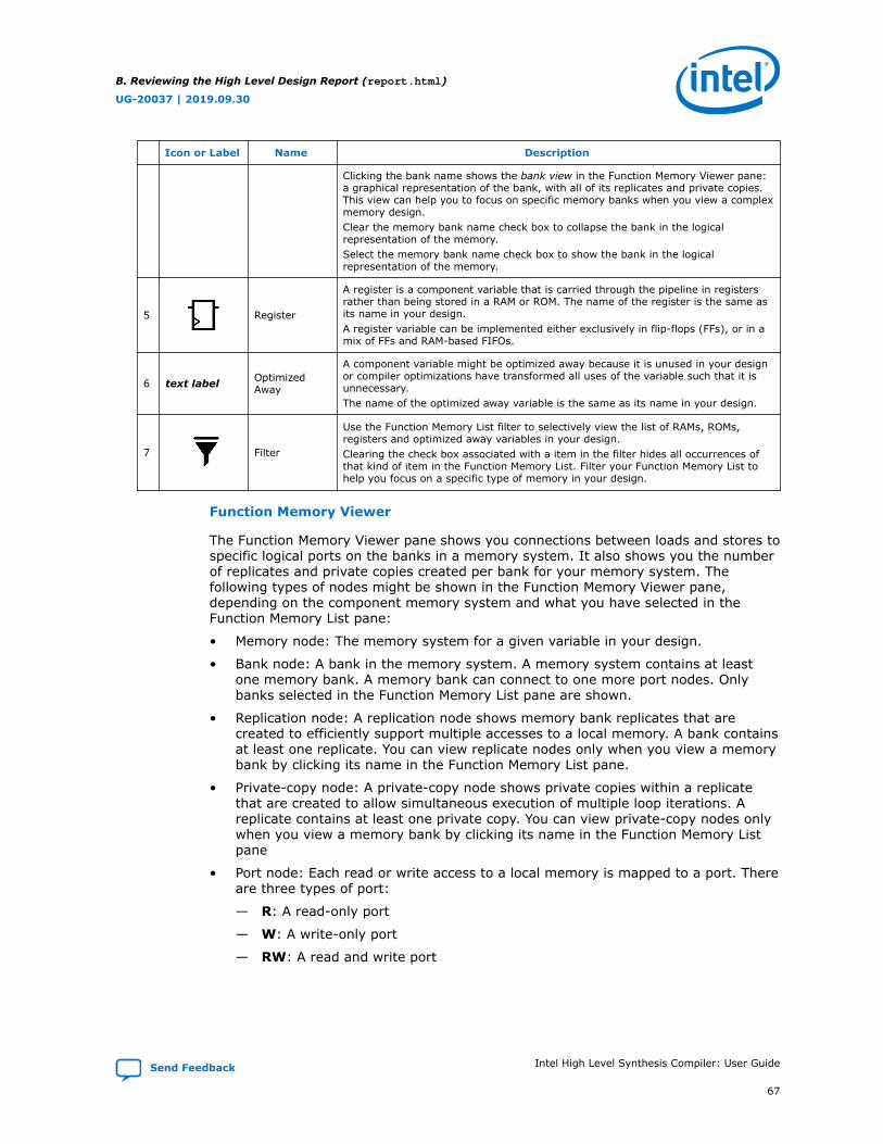
Icon or Label Name Description
Clicking the bank name shows the bank view in the Function Memory Viewer pane:a graphical representation of the bank, with all of its replicates and private copies.This view can help you to focus on specific memory banks when you view a complexmemory design.Clear the memory bank name check box to collapse the bank in the logicalrepresentation of the memory.Select the memory bank name check box to show the bank in the logicalrepresentation of the memory.
5 Register
A register is a component variable that is carried through the pipeline in registersrather than being stored in a RAM or ROM. The name of the register is the same asits name in your design.A register variable can be implemented either exclusively in flip-flops (FFs), or in amix of FFs and RAM-based FIFOs.
6 text label OptimizedAway
A component variable might be optimized away because it is unused in your designor compiler optimizations have transformed all uses of the variable such that it isunnecessary.The name of the optimized away variable is the same as its name in your design.
7 Filter
Use the Function Memory List filter to selectively view the list of RAMs, ROMs,registers and optimized away variables in your design.Clearing the check box associated with a item in the filter hides all occurrences ofthat kind of item in the Function Memory List. Filter your Function Memory List tohelp you focus on a specific type of memory in your design.
Function Memory Viewer
The Function Memory Viewer pane shows you connections between loads and stores tospecific logical ports on the banks in a memory system. It also shows you the numberof replicates and private copies created per bank for your memory system. Thefollowing types of nodes might be shown in the Function Memory Viewer pane,depending on the component memory system and what you have selected in theFunction Memory List pane:
• Memory node: The memory system for a given variable in your design.
• Bank node: A bank in the memory system. A memory system contains at leastone memory bank. A memory bank can connect to one more port nodes. Onlybanks selected in the Function Memory List pane are shown.
• Replication node: A replication node shows memory bank replicates that arecreated to efficiently support multiple accesses to a local memory. A bank containsat least one replicate. You can view replicate nodes only when you view a memorybank by clicking its name in the Function Memory List pane.
• Private-copy node: A private-copy node shows private copies within a replicatethat are created to allow simultaneous execution of multiple loop iterations. Areplicate contains at least one private copy. You can view private-copy nodes onlywhen you view a memory bank by clicking its name in the Function Memory Listpane
• Port node: Each read or write access to a local memory is mapped to a port. Thereare three types of port:
— R: A read-only port
— W: A write-only port
— RW: A read and write port
B. Reviewing the High Level Design Report (report.html)
UG-20037 | 2019.09.30
Send Feedback Intel High Level Synthesis Compiler: User Guide
67

• LSU node: A store (ST) or load (LD) node connected to the memory through portnodes.
• Arbitration node: An arbitration (ARB) node shows that LSUs compete for accessto a shared port node,which can lead to stalls.
• Port-sharing node: A port-sharing node (SHARE) shows that LSUs have mutuallyexclusive access to a shared port node, so the load-store units are free from stalls.
Hover over any node to view the attributes of that node.
Hover over an LSU node to highlight the path from the LSU node to all of the portsthat the LSU connects to.
Hover over a port node to highlight the path from the port node to all of the LSUs thatread or write to the port node.
Click a node to select it and have the node attributes displayed in the Details pane.
The following figures show examples of what you can see in the Function MemoryViewer:Logical representation of a memory in the Function Memory Viewer pane
B. Reviewing the High Level Design Report (report.html)
UG-20037 | 2019.09.30
Intel High Level Synthesis Compiler: User Guide Send Feedback
68

Bank view of a memory bank in the Function Memory Viewer pane
Code View
The code view pane shows your source code. Clicking on a memory or a bank in theFunction Memory Viewer pane highlights the line of your code (in the code view pane)where you declared the memory.
Details
The Details pane shows the attributes of the node selected in the Function MemoryViewer pane. For example, when you select a memory in a component, the Detailspane shows information such as the width and depths of the memory banks, thememory layout information, the address bit mapping and any user-defined HLSattributes that you specified in your source code.
The content of the Details pane persists until you select a different node in theComponent/Function Memory Viewer pane.
B.5.3. Schedule Viewer (Alpha)
Use the Schedule Viewer to identify latency bottlenecks in your design. The ScheduleViewer shows the estimated start and ending clock cycle for functions, blocks,clusters, and individual instructions in your design.
Click on an item in the Schedule List to focus the Schedule View at the selected level.You cannot on the system level of the component hierarchy in the Schedule List.
Click the schedule bar for an item in the Schedule View updates the Details pane withthe information available about that item. The information can include a description ofthe item, its start cycle, and its latency.
Click an item in the Schedule View to show a popup menu for the item. Forinstructions, the popup menu includes a link that takes you to your C++ code thatresulted in that instruction.
B. Reviewing the High Level Design Report (report.html)
UG-20037 | 2019.09.30
Send Feedback Intel High Level Synthesis Compiler: User Guide
69

B.6. Viewing Component Design
The High Level Design Report (report.html) contains reports that show differentviews into the structure, interfaces, datapaths, and computation flows in yourcomponent.
The reports represent your component and tasks as a system of functions. Eachfunction is represented by a set of blocks. Inside each block is a set of non-branchinginstructions that covers your code and the compiler loop orchestration optimization.The connections between blocks show the execution flow of your component.
There is an initialization block, called the runOnce block. When a component containsloops, cycles of blocks form, depending on the loop structure. Loops often imposeinitiation interval (II) bottlenecks and are a main optimization focus when youoptimize your component.
A component block has three main parts:
• An input or loop input node
• A set of instructions
• A branch node
The input node and the branch node might not be present depending on if there isbranching in or out of the block. The input or loop input node determines the initialvalue for variables depending on where the branch into this block is from. The rest ofthe block should ideally be filled with non-stallable instructions and have a minimalamount of stallable instructions, like I/O instructions or memory access instructions.
To save the amount of control handshaking infrastructure needed when synthesizingyour design, the Intel HLS Compiler groups instructions within a block into groupscalled clusters. A cluster has an entry and exit node to handle the controlhandshaking. There is no further control handshaking within a cluster.
The Intel HLS Compiler can create two types of clusters:
• Stall-free clusters
A stall-free cluster contains nonstallable instructions, and has a FIFO to store datathat needs to be passed to logic outside of the cluster. The FIFO information isshown in the cluster exit node when you examine the cluster in the Cluster Viewer.
• Stall-enable clusters
A stall-enable cluster contains stallable instructions.
A branch node indicates the next block to go to and the condition required to go tothat block.
The views of your components are split into different reports. The reports available toyou depend on your edition of the Intel HLS Compiler.
The Intel HLS Compiler Standard Edition provides the following reports about yourcomponent design:
B. Reviewing the High Level Design Report (report.html)
UG-20037 | 2019.09.30
Intel High Level Synthesis Compiler: User Guide Send Feedback
70

• Component Viewer
The Component Viewer report shows branching in your component.
• Component Memory Viewer
The Component Memory Viewer report shows the data connections across thememory system of your component.
B.6.1. Reviewing Component Interfaces
The Component Viewer shows a visual representation of the interfaces in yourcomponent. You can view details about the following interface arguments: default,pointer, pass-by-reference, Avalon Memory-Mapped (MM), and Avalon Streaming.
Some interface arguments in your component can be marked as being stable. A stableinterface argument is an argument that does not change while your componentexecutes, but the argument might change between component executions. In theComponent Viewer, a stable node does not have any edge connection.
The Component Viewer displays the different interfaces as outlined in the followingsections:
• Default Interface Arguments on page 71
• Pointer, Pass-By-Reference, and Avalon MM Master Interface Arguments on page73
• Avalon MM Slave Register Interface Arguments on page 75
• Avalon MM Slave Memory Interface Arguments on page 77
• Avalon Streaming Interface Arguments on page 79
Default Interface Arguments
Default interface arguments are any scalars or simple structs. The Component Viewerconnects the default argument nodes to the corresponding channel read (RD) node.
#include "HLS/hls.h"#include "stdio.h"
struct coordinate_t { int x; int y;};
component int default_comp(int b, coordinate_t p) { return b + p.x;}
B. Reviewing the High Level Design Report (report.html)
UG-20037 | 2019.09.30
Send Feedback Intel High Level Synthesis Compiler: User Guide
71

For each default interface argument node, you can view details about the node whenyou hover over the node:
B. Reviewing the High Level Design Report (report.html)
UG-20037 | 2019.09.30
Intel High Level Synthesis Compiler: User Guide Send Feedback
72

Pointer, Pass-By-Reference, and Avalon MM Master Interface Arguments
Pointer interfaces, pass-by-reference interfaces, Avalon MM master interfaces, andglobal variables all correspond to addresses to memory outside of your component.Similarly to the default interface arguments, these nodes connect to the correspondingchannel read (RD) node for your component.
#include "HLS/hls.h"#include "stdio.h"
component int master_comp( int *pointer_d, ihc::mm_master<int, ihc::aspace<3>, ihc::awidth<4>, ihc::dwidth<32>,ihc::latency<1>, ihc::align<4> > &master_i, int &result ) { result = *pointer_d + *master_i; return result;}
B. Reviewing the High Level Design Report (report.html)
UG-20037 | 2019.09.30
Send Feedback Intel High Level Synthesis Compiler: User Guide
73

The Component Viewer shows the following details for these interface arguments:
Stable Describes whether the interface argument is stable. That is, whetherthe hls_stable_argument attribute was applied.
Data width The width of the memory-mapped data bus in bits.
Address width The width of the memory-mapped address bus in bits.
Latency The guaranteed latency from when the read command exits thecomponent to when the external memory returns valid read data.The latency is measured in clock cycles.
Maximumburst
The maximum number of data transfers that can associate with aread or write transaction. For fixed latency interfaces, this value isset to 1.
Alignment The byte alignment of the base pointer address. The Intel HLSCompiler uses this information to determine the amount ofcoalescing that is possible for loads and stores to this pointer.
B. Reviewing the High Level Design Report (report.html)
UG-20037 | 2019.09.30
Intel High Level Synthesis Compiler: User Guide Send Feedback
74

The Component Viewer shows the following details for global memories:
Memory address spacenumber
The memory address space number for global memory.
Number of banks The number of memory banks contained in thememory.
Argument Name: The names of arguments that access the globalmemory.
Avalon MM Slave Register Interface Arguments
When you label an interface argument as an Avalon MM slave register(hls_avalon_slave_register_argument), then the interface argument isimplemented in the control and status register (CSR) slave interface. The ComponentViewer puts the slave register arguments inside a CSR container.
#include "HLS/hls.h"#include "stdio.h"
component int slavereg_comp( int hls_avalon_slave_register_argument slave_scalar_f, int* hls_avalon_slave_register_argument slave_pointer_g
B. Reviewing the High Level Design Report (report.html)
UG-20037 | 2019.09.30
Send Feedback Intel High Level Synthesis Compiler: User Guide
75

) { return slave_scalar_f + *slave_pointer_g;}
The resulting memory map is described in the automatically generated header file<component_name>_csr.h. This header file is available in the menu in the sourcecode pane. Clicking on the CSR container node in the Component Viewer also opensup the header file:
B. Reviewing the High Level Design Report (report.html)
UG-20037 | 2019.09.30
Intel High Level Synthesis Compiler: User Guide Send Feedback
76

If you use the hls_avalon_slave_component macro, then the “do” and “return”streams (control and status registers) are implemented in the CSR interface:
#include "HLS/hls.h"#include "stdio.h"
hls_avalon_slave_componentcomponent int slavereg_comp( int hls_avalon_slave_register_argument slave_scalar_f, int* hls_avalon_slave_register_argument slave_pointer_g ) { return slave_scalar_f + *slave_pointer_g;}
Avalon MM Slave Memory Interface Arguments
When you declare a pointer argument as a slave memory, the Component Viewershows the slave memory interface with a <slave memory name> LD/ST node thatis connected to the Local Memory node in the component.
#include "HLS/hls.h"#include "stdio.h"
B. Reviewing the High Level Design Report (report.html)
UG-20037 | 2019.09.30
Send Feedback Intel High Level Synthesis Compiler: User Guide
77

hls_avalon_slave_componentcomponent int slavemem_comp( hls_avalon_slave_memory_argument(4096) int* slave_mem_h, int index, int hls_avalon_slave_register_argument slave_scalar_f ) { return slave_mem_h[index] * slave_scalar_f;}
If you look at the same Avalon MM slave memory interface in the Component MemoryViewer report, the same <slave memory name> LD/ST node is shown to beconnected to an external RW port.
B. Reviewing the High Level Design Report (report.html)
UG-20037 | 2019.09.30
Intel High Level Synthesis Compiler: User Guide Send Feedback
78

Avalon Streaming Interface Arguments
A streaming interface is shown in the Component Viewer by a <stream name> nodeconnected to the corresponding RD node (for stream_in<>) or WR node (forstream_out<>).
#include "HLS/hls.h"#include "stdio.h"component int stream_comp( ihc::stream_in<int> &stream_in_c, ihc::stream_out<int> &stream_out_e, int scalar_b ) {
stream_out_e.write(scalar_b + 1); return stream_in_c.read() + scalar_b * 2;}
B. Reviewing the High Level Design Report (report.html)
UG-20037 | 2019.09.30
Send Feedback Intel High Level Synthesis Compiler: User Guide
79
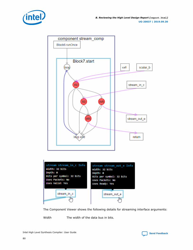
The Component Viewer shows the following details for streaming interface arguments:
Width The width of the data bus in bits.
B. Reviewing the High Level Design Report (report.html)
UG-20037 | 2019.09.30
Intel High Level Synthesis Compiler: User Guide Send Feedback
80

Depth The depth of the stream in words
The word size of the stream is the size of the stream datatype.
Bits persymbol
Describes how the data is broken into symbols on the data bus.
Uses Packets Indicates whether the interface exposes the startofpacket andendofpacket sideband signals on the stream interfaces. The signalscan be access by the packet-based reads and writes.
Uses Valid (stream_in) Indicates whether a valid signal is present on thestream interface. When Yes, the upstream source must provide validdata on every cycle that ready is asserted.
Uses Reader (stream_in) Indicates whether a ready signal is present on thestream interface. When Yes, the downstream sink must be able toaccept data on every cycle that valid is asserted.
B.6.2. Reviewing Memory Replication and Stallable LSU Information
The Component Viewer report in the High Level Design Report (report.html) showsan abstracted netlist of your kernel design. In the Component Viewer, you canvisualize load-store units (LSUs) between a component and different memories,streams, and loops.
Consider the following code excerpt from the transpose_and_fold component (partof the tutorial files provided in <QPDS_installdir>/hls/examples/tutorials/loop_memory_dependency):
01 #include "HLS/hls.h"02 #include "stdio.h"03 #include "stdlib.h"04 05 #define SIZE 3206 07 typedef altera::stream_in<int> my_operand;08 typedef altera::stream_out<int> my_result;09 10 void transpose_and_fold(my_operand &a, my_operand &b, my_result &c)11 {12 int i;13 int j;14 int a_buf[SIZE][SIZE];15 int b_buf[SIZE][SIZE];16 for (i = 0; i < SIZE * SIZE; i++) {17 a_buf[i / SIZE][i % SIZE] = a.read();18 b_buf[i / SIZE][i % SIZE] = b.read();19 }20 #ifdef USE_IVDEP21 #pragma ivdep22 #endif23 for (j = 0; j < SIZE * SIZE * SIZE; j++) {24 #pragma unroll25 for (i = 0; i < SIZE; i++) {26 b_buf[j % SIZE][i] += a_buf[i][j % SIZE];27 }28 }29 for (i = 0; i < SIZE * SIZE; i++) {
B. Reviewing the High Level Design Report (report.html)
UG-20037 | 2019.09.30
Send Feedback Intel High Level Synthesis Compiler: User Guide
81

30 c.write(b_buf[i / SIZE][i % SIZE]);31 }32 }
The figure below shows that Block3 is highlighted in red to prompt you to review theloop. Because loop analysis of Block3 shows that it is a pipelined loop with an IIvalue of 2, the loop pipeline might affect the throughput of your design. TheComponent Viewer shows that the II value is caused by a memory dependency onloads to the b_buf variable.
Figure 10. Component View of the transpose_and_fold Component
B. Reviewing the High Level Design Report (report.html)
UG-20037 | 2019.09.30
Intel High Level Synthesis Compiler: User Guide Send Feedback
82

By hovering your mouse pointer over a node, you can view the tooltip and details thatprovide more information on the LSU. In the figure below, the tooltip showsinformation like the latency and that the LSU is stall-free.
Figure 11. Detailed View of Node and Tooltip
The Component Viewer allows you to select the type of connections you want to view.Selecting Control instructs the system viewer to display the connections betweenblocks and loops. Selecting Memory instructs the function view of the Graph Viewerto display the connections to and from global and local memories. Selecting Streamsinstructs the system viewer to display the connections reading from and writing tostreams.
B. Reviewing the High Level Design Report (report.html)
UG-20037 | 2019.09.30
Send Feedback Intel High Level Synthesis Compiler: User Guide
83

Figure 12. Component View of the transpose_and_fold Component without Connectionsbetween Blocks and Loops
B.6.3. Viewing Your Component Memory System
Data movement is a bottleneck in many algorithms. The Component Memory Viewer inthe High Level Design Report (report.html) shows you how the Intel HLS CompilerStandard Edition interprets the data connections across the memory system of yourcomponent. Use the Component Memory Viewer to help you identify data movementbottlenecks in your component design.
B. Reviewing the High Level Design Report (report.html)
UG-20037 | 2019.09.30
Intel High Level Synthesis Compiler: User Guide Send Feedback
84

Some patterns in memory accesses can cause undesired arbitration in the load-storeunits (LSUs), which can affect the throughput performance of your component. Usethe Component Memory Viewer to find where you might have unwanted arbitration inthe LSUs.
The Component Memory Viewer has the following panes:
Memory List The Memory List pane shows you a hierarchy of components,memories in that component, and the corresponding memory banks.
Clicking a memory name in the list displays a graphical representationof the memory in the Component memory viewer pane. Also, the linein your code where you declared the memory is highlighted in theSource Code pane.
Clearing a check box for a memory bank collapses that bank in theComponent Memory Viewer pane, which can help you to focus onspecific memory banks when you view a complex memory design. Bydefault, all banks in component memory are selected and shown in theComponent Memory Viewer pane.
B. Reviewing the High Level Design Report (report.html)
UG-20037 | 2019.09.30
Send Feedback Intel High Level Synthesis Compiler: User Guide
85

ComponentMemoryViewer
The Component Memory Viewer pane shows you connections betweenloads and stores to specific logical ports on the banks in a memorysystem. The following types of nodes might be shown in theComponent Memory Viewer pane, depending on the componentmemory system:
• Memory node: The component memory.
• Bank node: A bank in the memory. Only banks selected in theMemory List pane are shown. Select banks in the Memory Listpane to help you focus on specific memory banks when you view acomplex memory design.
• Port node: The logical port for a bank. There are three types ofport:
— R: A read-only port
— W: A write-only port
— RW: A read and write port
• LSU node: A store (ST) or load (LD) node connected to thememory.
• Arbitration node: An arbitration (ARB) node shows that LSUscompete for access to a shared port node,which can lead to stalls.
• Port-sharing node: A port-sharing node (SHARE) shows that LSUshave mutually exclusive access to a shared port node, so the load-store units are free from stalls.
Hover over any node to view the attributes of that node.
Hover over an LSU node to highlight the path from the LSU node to allof the ports that the LSU connects to.
Hover over a port node to highlight the path from the port node to allof the LSUs that store to the port node.
Click a node to select it and have the node attributes displayed in theDetails pane.
Details The Details pane shows the attributes of the node selected in theComponent Memory Viewer pane. For example, when you select amemory in a component, the Details pane shows information such asthe width and depths of the memory banks, as well as any user-defined HLS attributes that you specified in your source code.
The content of the Details pane persists until you select a differentnode in the Component Memory Viewer pane.
B.7. Reviewing Your Component Verification Results
For each component that the testbench calls, the verification statistics report providesinformation such as the number and type of invocations, latency, initiation interval,and throughput.
The verification statistics report becomes available after you simulate your component.
B. Reviewing the High Level Design Report (report.html)
UG-20037 | 2019.09.30
Intel High Level Synthesis Compiler: User Guide Send Feedback
86

Important: • The data presented in the verification statistics report might be dependent on theinput values to the component from the test bench.
• The verification statistics report only reports the component loop initiation interval(II) values and throughput for enqueued invocations.
The following example verification statistics report is for a component dut that hasbeen run once as a simple function call and 100 times as an enqueued invocation:
For components that use explicit streams, such as ihc::stream_in<> orihc::stream_out<>, the verification statistics report also provides the throughputfor each individual stream, as shown in the details pane:
B.8. Accessing HLD FPGA Reports in JSON Format
The high level design report data for the Intel HLS Compiler is also available as JSON-formatted data.
The JSON files containing the data are available in the <result>.prj/reports/lib/json directory. The directory provides the following .json files:
Table 5. JSON Files in the <result>.prj/reports/lib/json Directory
File Description
area.json Area Analysis of System
area_src.json Area Analysis of Source
block.jsonBlock view of Graph Viewer
info.json Summary
loops.json Loop Analysis
mav.jsonFunction View of Graph Viewer
Component Viewer
lmv.jsonComponent Memory Viewer
continued...
B. Reviewing the High Level Design Report (report.html)
UG-20037 | 2019.09.30
Send Feedback Intel High Level Synthesis Compiler: User Guide
87

File Description
new_lmv.jsonFunction Memory Viewer
pipeline.jsonCluster View of Graph Viewer
quartus.json Summary
summary.json Summary
system.jsonSystem View of Graph Viewer
warnings.json Summary
You can read the following .json files without a special parser:
• area.json
• area_src.json
• loops.json
• quartus.json
• summary.json
For example, if you want to identify all of the values and bottlenecks for the initiationinterval (II) of a loop, you can find the information in the children section in theloops.json file, as shown below:
“name”:”<block name|Component: component name> # Find the loops which does not begin with “Component:” “data”:[<Yes|No>, <#|n/a>, <II|n/a>] # The data field corresponds to “Pipelined”, “II”, “Bottleneck”
B. Reviewing the High Level Design Report (report.html)
UG-20037 | 2019.09.30
Intel High Level Synthesis Compiler: User Guide Send Feedback
88