Embed Size (px)
Citation preview
Intel® Aero Compute Board
Hardware Features and Usage Rev 1.5.2
2
INFORMATION IN THIS DOCUMENT IS PROVIDED IN CONNECTION WITH INTEL® PRODUCTS. NO LICENSE, EXPRESS OR IMPLIED,
BY ESTOPPEL OR OTHERWISE, TO ANY INTELLECTUAL PROPERTY RIGHTS IS GRANTED BY THIS DOCUMENT. EXCEPT AS PROVIDED
IN INTEL’S TERMS AND CONDITIONS OF SALE FOR SUCH PRODUCTS, INTEL ASSUMES NO LIABILITY WHATSOEVER, AND INTEL DISCLAIMS ANY EXPRESS OR IMPLIED WARRANTY, RELATING TO SALE AND/OR USE OF INTEL PRODUCTS INCLUDING LIABILITY
OR WARRANTIES RELATING TO FITNESS FOR A PARTICULAR PURPOSE, MERCHANTABILITY, OR INFRINGEMENT OF ANY PATENT,
COPYRIGHT OR OTHER INTELLECTUAL PROPERTY RIGHT.
UNLESS OTHERWISE AGREED IN WRITING BY INTEL, THE INTEL PRODUCTS ARE NOT DESIGNED NOR INTENDED FOR ANY
APPLICATION IN WHICH THE FAILURE OF THE INTEL PRODUCT COULD CREATE A SITUATION WHERE PERSONAL INJURY OR DEATH
MAY OCCUR.
Intel may make changes to specifications and product descriptions at any time, without notice. Designers must not rely on the
absence or characteristics of any features or instructions marked “reserved” or “undefined.” Intel reserves these for future definition
and shall have no responsibility whatsoever for conflicts or incompatibilities arising from future changes to them. The information
here is subject to change without notice. Do not finalize a design with this information.
The products described in this document may contain design defects or errors known as errata which may cause the product to
deviate from published specifications. Current characterized errata are available on request.
Contact your local Intel sales office or your distributor to obtain the latest specifications and before placing your product order.
Intel, Atom, RealSense, MAX and the Intel logo are trademarks of Intel Corporation in the U.S. and other countries.
*Other names and brands may be claimed as the property of others.
Copyright © 2017, Intel Corporation. All rights reserved.
3
Contents
1 Introduction ...................................................................................................... 5
2 Intel® Aero Compute Board Block Diagram ........................................................... 6
3 Connector Specifications ..................................................................................... 7
3.1 Connector Part Numbers .......................................................................... 7 3.2 Connector Locations and Pin Orientation .................................................... 7 3.3 8MP Camera Connector ........................................................................... 8
3.3.1 Connector Pin Definition ............................................................. 8 3.4 VGA Camera Connector ........................................................................... 8
3.4.1 Connector Pin Definition ............................................................. 8 3.5 RealSense USB 3.0 Camera Connector ...................................................... 9
3.5.1 Connector Pin Definition ............................................................. 9 3.5.2 Software Access ........................................................................ 9
3.6 Power & UART Connector ......................................................................... 9 3.6.1 Connector Pin Definition ........................................................... 10 3.6.2 Software Access to the Processor HSUART .................................. 10
3.7 IO Expansion Connector ........................................................................ 10 3.7.1 Connector Pin Definition ........................................................... 10 3.7.2 Software Access ...................................................................... 11
3.8 80-pin Accessories Connector Pinout Definition ......................................... 13 3.8.1 “J1” Power Board ..................................................................... 13 3.8.2 “J2” Radio Control ................................................................... 14 3.8.3 “J3” GPS ................................................................................. 14 3.8.4 “J4” Compass .......................................................................... 14 3.8.5 “J5” Telemetry ........................................................................ 14
4 On-Board Sensors............................................................................................ 15
5 LED Definition and Usage .................................................................................. 16
5.1 Compute Board LEDs ............................................................................. 16 5.2 Compute Board Top Side LED Locations ................................................... 17 5.3 Compute Board Bottom Side LED Locations .............................................. 18
6 Intel® Aero Flight Controller .............................................................................. 19
4
Revision History
Revision Number
Description Revision Date
1.0 Initial release February 2017
1.5 Updated the block diagram (Figure 1)
Corrected SPI1 chip-select assignments CS-0 and CS-1
Added detail for Intel® Aero Flight Controller interfaces
Updated the voltage input requirement section 3.6.1
Added CAN bus pin assignments to the table in section 3.7.1
Added a new section discussing the Intel® Aero Flight Controller which is assembled with the Intel® Aero Compute Board inside the Intel® Aero Ready to Fly Drone (section 6)
July 2017
1.5.1 Corrected reference to chip selects in body of text 3.7.1 to match the block diagram in Figure 1
February 2018
1.5.2 Corrected CPU kernel GPIO # and pin assignments in sections 3.7.1 and 3.7.2.2
Updated URL references throughout the document
Eliminated one subsection in section 5 that was sufficiently addressed in 5.1
Corrected the pin numbering for the 80-pin IO Expansion Connector in Figure 2 and Figure 7
April 2018
Introduction
5
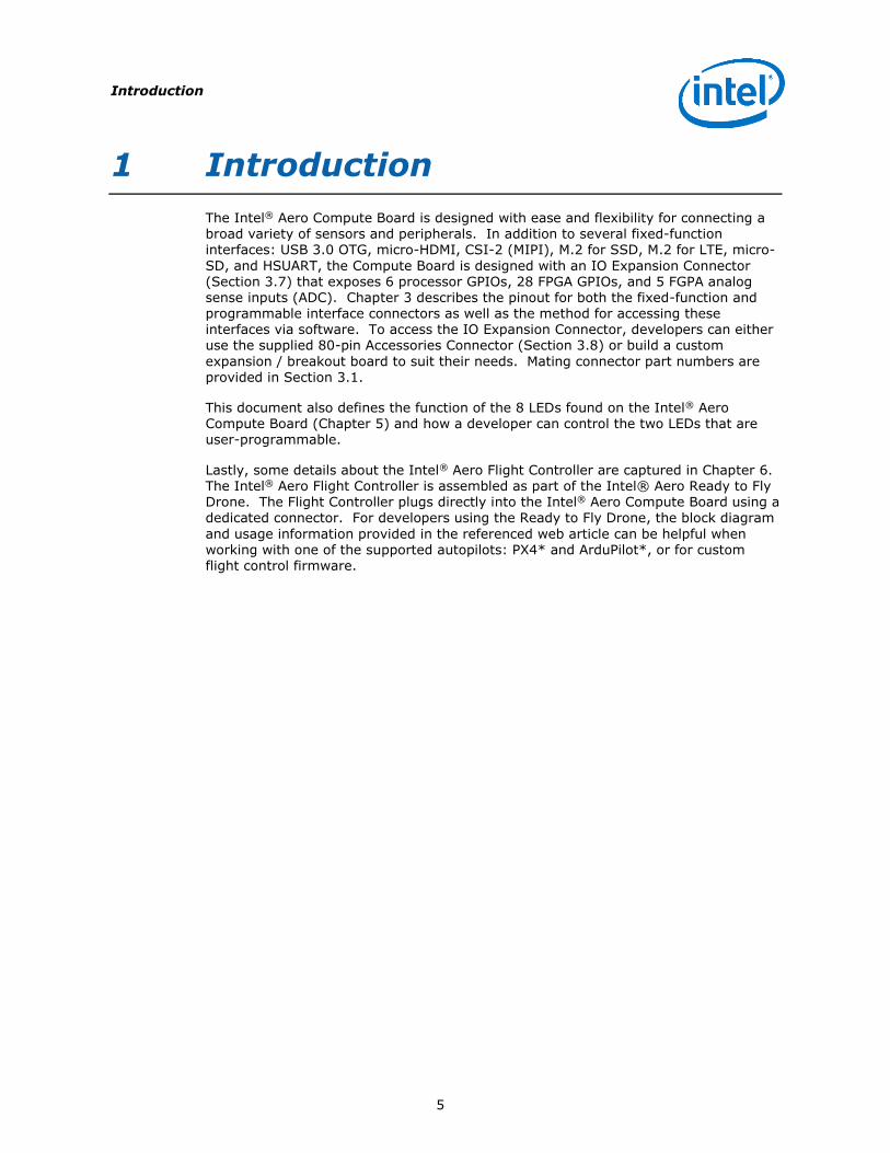
1 Introduction
The Intel® Aero Compute Board is designed with ease and flexibility for connecting a broad variety of sensors and peripherals. In addition to several fixed-function interfaces: USB 3.0 OTG, micro-HDMI, CSI-2 (MIPI), M.2 for SSD, M.2 for LTE, micro-
SD, and HSUART, the Compute Board is designed with an IO Expansion Connector (Section 3.7) that exposes 6 processor GPIOs, 28 FPGA GPIOs, and 5 FGPA analog sense inputs (ADC). Chapter 3 describes the pinout for both the fixed-function and programmable interface connectors as well as the method for accessing these interfaces via software. To access the IO Expansion Connector, developers can either use the supplied 80-pin Accessories Connector (Section 3.8) or build a custom
expansion / breakout board to suit their needs. Mating connector part numbers are
provided in Section 3.1.
This document also defines the function of the 8 LEDs found on the Intel® Aero Compute Board (Chapter 5) and how a developer can control the two LEDs that are user-programmable.
Lastly, some details about the Intel® Aero Flight Controller are captured in Chapter 6. The Intel® Aero Flight Controller is assembled as part of the Intel® Aero Ready to Fly Drone. The Flight Controller plugs directly into the Intel® Aero Compute Board using a dedicated connector. For developers using the Ready to Fly Drone, the block diagram
and usage information provided in the referenced web article can be helpful when working with one of the supported autopilots: PX4* and ArduPilot*, or for custom flight control firmware.
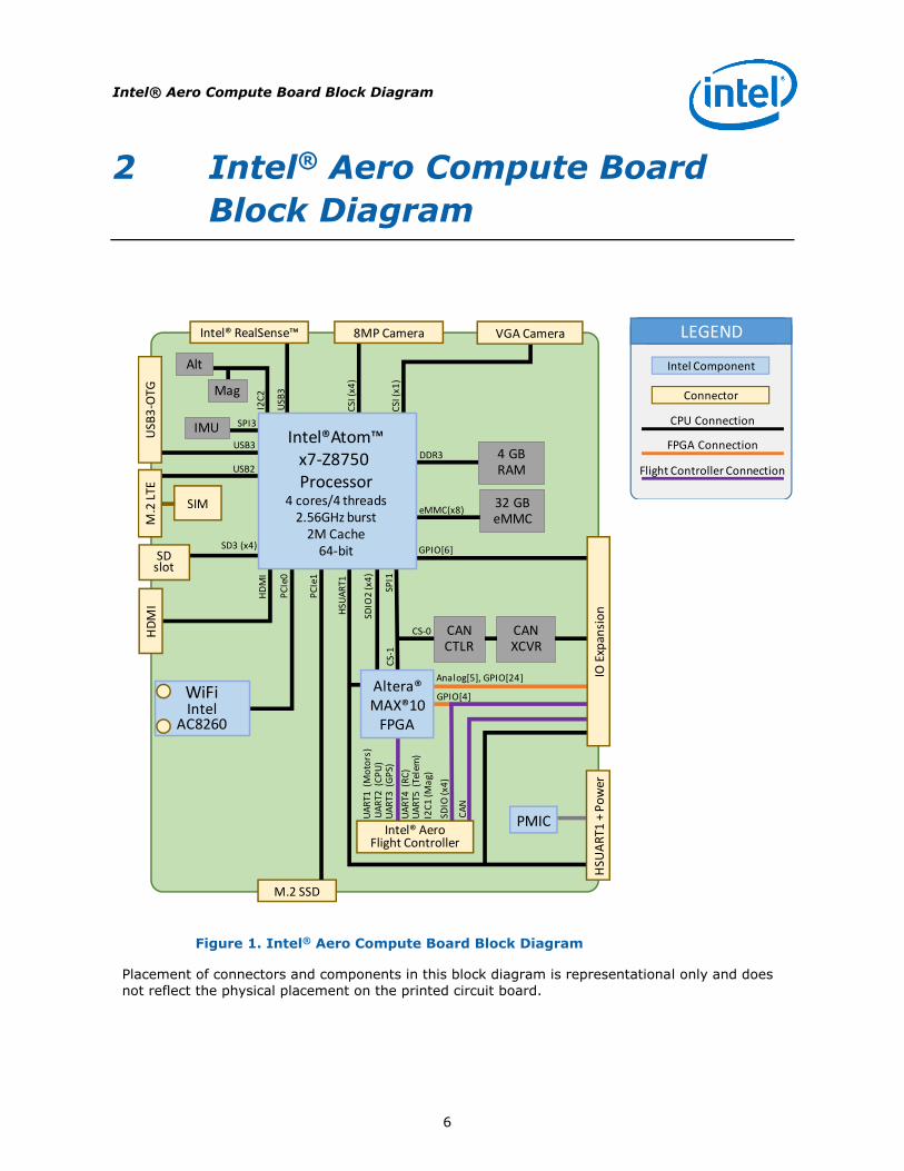
Intel® Aero Compute Board Block Diagram
6
2 Intel® Aero Compute Board
Block Diagram
Figure 1. Intel® Aero Compute Board Block Diagram
Placement of connectors and components in this block diagram is representational only and does
not reflect the physical placement on the printed circuit board.
Connector
CPU Connection
FPGA Connection
Flight Controller Connection
LEGEND
Intel Component
USB
3-O
TG
M.2 SSD
SIM
CANCTLR
CANXCVR
DDR3
CSI
(x1
)
CSI
(x4
)
USB
3P
CIe
0
SPI1
HSU
AR
T1
32 GBeMMC
eMMC(x8)
Analog[5], GPIO[24]
GPIO[6]SD3 (x4)
PC
Ie1
USB3
HD
MI
SDIO
(x4
)
USB2
SPI3
I2C
2
CS-
1
CS-0
SDIO
2 (x
4)
M.2
LTE
HSU
AR
T1 +
Po
wer
WiFiIntel
AC8260
Intel®Atom™x7-Z8750Processor
4 cores/4 threads2.56GHz burst
2M Cache64-bit
4 GBRAM
HD
MI
SDslot
Alt
IMU
Mag
Intel® RealSense™ VGA Camera8MP Camera
PMIC
Altera® MAX®10
FPGA
GPIO[4]
UA
RT2
(C
PU
)U
AR
T1 (
Mo
tors
)
UA
RT3
(G
PS)
I2C
1 (M
ag)
UA
RT4
(R
C)
UA
RT5
(Te
lem
)
CA
N
IO E
xpan
sio
n
Intel® Aero Flight Controller
Connector Specifications
7
3 Connector Specifications
Users may connect various devices to the Compute Board by building a custom cable using the connector information provided in Section 3.1 and the pin definitions captured in Chapter 3.
3.1 Connector Part Numbers
Connector Manufacturer
Name Manufacturer Part
Number Mating Connector
Part Number
Front Facing 8MP Camera
JAE Electronics WP7A-S030VA1-R500 WP7-P030VA1-R500
Down Facing VGA Camera
Advanced Connectek BBR43-24KB533 BBR13-24K6417
RealSense USB3.0 Camera
Dai-Ichi Seiko 20347-310E-12R 20347-310E-12R
Power and Console UART
Molex 53261-1071 51021-1000
IO Expansion JST 80PS-JMDSS-G-1-TF 80R-JMDSS-G-1-TF
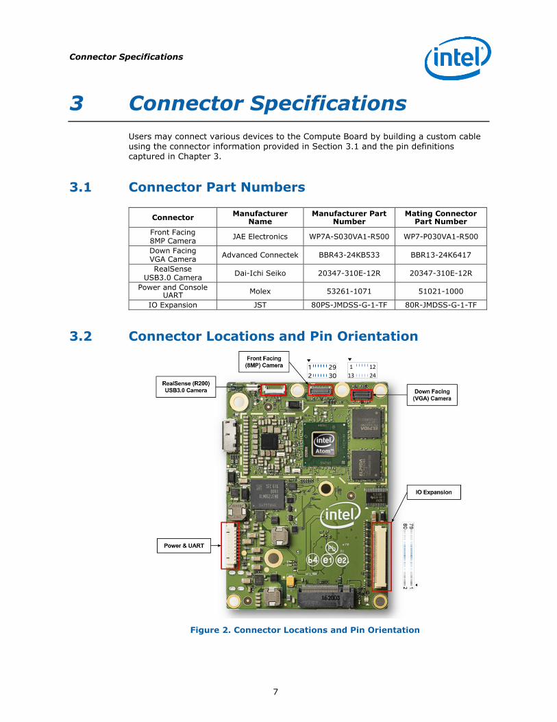
3.2 Connector Locations and Pin Orientation
Figure 2. Connector Locations and Pin Orientation
1 29
2 30
1 12 13 24
Connector Specifications
8
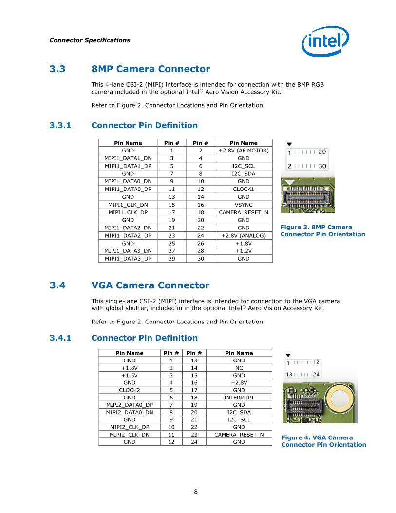
3.3 8MP Camera Connector
This 4-lane CSI-2 (MIPI) interface is intended for connection with the 8MP RGB
camera included in the optional Intel® Aero Vision Accessory Kit.
Refer to Figure 2. Connector Locations and Pin Orientation.
3.3.1 Connector Pin Definition
Pin Name Pin # Pin # Pin Name
GND 1 2 +2.8V (AF MOTOR)
MIPI1_DATA1_DN 3 4 GND
MIPI1_DATA1_DP 5 6 I2C_SCL
GND 7 8 I2C_SDA
MIPI1_DATA0_DN 9 10 GND
MIPI1_DATA0_DP 11 12 CLOCK1
GND 13 14 GND
MIPI1_CLK_DN 15 16 VSYNC
MIPI1_CLK_DP 17 18 CAMERA_RESET_N
GND 19 20 GND
MIPI1_DATA2_DN 21 22 GND
MIPI1_DATA2_DP 23 24 +2.8V (ANALOG)
GND 25 26 +1.8V
MIPI1_DATA3_DN 27 28 +1.2V
MIPI1_DATA3_DP 29 30 GND
Figure 3. 8MP Camera Connector Pin Orientation
3.4 VGA Camera Connector
This single-lane CSI-2 (MIPI) interface is intended for connection to the VGA camera
with global shutter, included in in the optional Intel® Aero Vision Accessory Kit.
Refer to Figure 2. Connector Locations and Pin Orientation.
3.4.1 Connector Pin Definition
Pin Name Pin # Pin # Pin Name
GND 1 13 GND
+1.8V 2 14 NC
+1.5V 3 15 GND
GND 4 16 +2.8V
CLOCK2 5 17 GND
GND 6 18 INTERRUPT
MIPI2_DATA0_DP 7 19 GND
MIPI2_DATA0_DN 8 20 I2C_SDA
GND 9 21 I2C_SCL
MIPI2_CLK_DP 10 22 GND
MIPI2_CLK_DN 11 23 CAMERA_RESET_N
GND 12 24 GND
Figure 4. VGA Camera Connector Pin Orientation
Connector Specifications
9
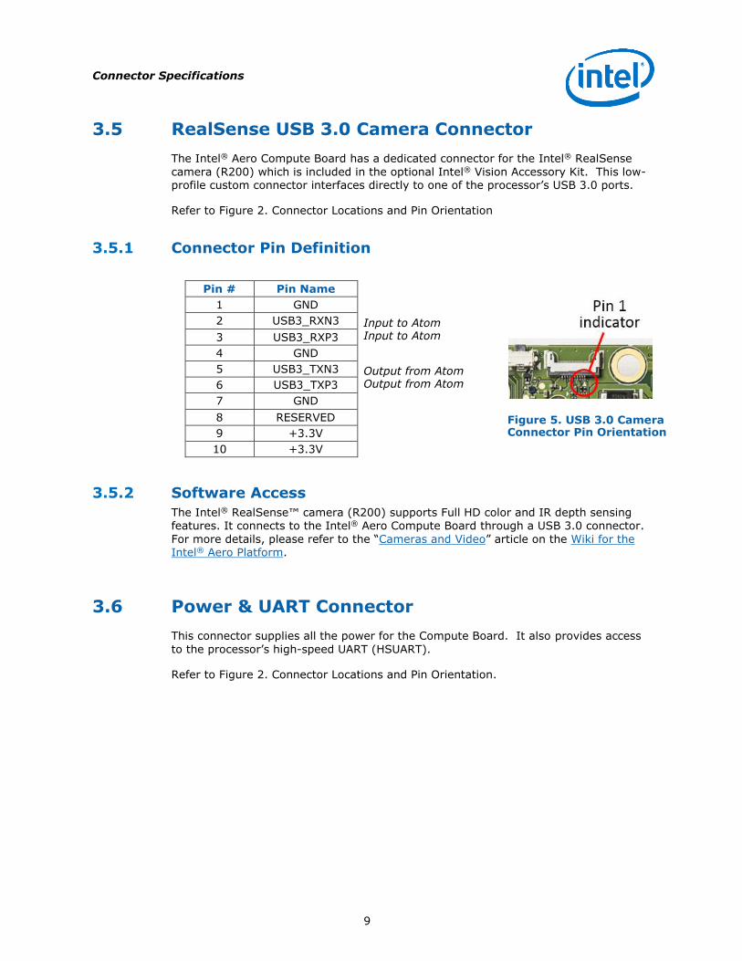
3.5 RealSense USB 3.0 Camera Connector
The Intel® Aero Compute Board has a dedicated connector for the Intel® RealSense
camera (R200) which is included in the optional Intel® Vision Accessory Kit. This low-profile custom connector interfaces directly to one of the processor’s USB 3.0 ports.
Refer to Figure 2. Connector Locations and Pin Orientation
3.5.1 Connector Pin Definition
Pin # Pin Name
1 GND
2 USB3_RXN3 Input to Atom Input to Atom 3 USB3_RXP3
4 GND
5 USB3_TXN3 Output from Atom Output from Atom 6 USB3_TXP3
7 GND
8 RESERVED
9 +3.3V
10 +3.3V
Figure 5. USB 3.0 Camera Connector Pin Orientation
3.5.2 Software Access
The Intel® RealSense™ camera (R200) supports Full HD color and IR depth sensing
features. It connects to the Intel® Aero Compute Board through a USB 3.0 connector.
For more details, please refer to the “Cameras and Video” article on the Wiki for the Intel® Aero Platform.
3.6 Power & UART Connector
This connector supplies all the power for the Compute Board. It also provides access
to the processor’s high-speed UART (HSUART).
Refer to Figure 2. Connector Locations and Pin Orientation.
Connector Specifications
10
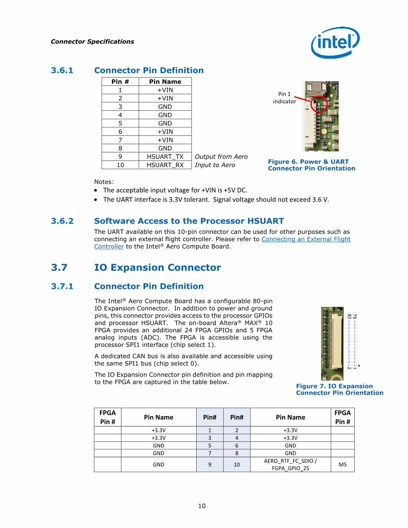
3.6.1 Connector Pin Definition
Pin # Pin Name
1 +VIN
2 +VIN
3 GND
4 GND
5 GND
6 +VIN
7 +VIN
8 GND
9 HSUART_TX Output from Aero
10 HSUART_RX Input to Aero
Figure 6. Power & UART Connector Pin Orientation
Notes:
The acceptable input voltage for +VIN is +5V DC.
The UART interface is 3.3V tolerant. Signal voltage should not exceed 3.6 V.
3.6.2 Software Access to the Processor HSUART
The UART available on this 10-pin connector can be used for other purposes such as
connecting an external flight controller. Please refer to Connecting an External Flight Controller to the Intel® Aero Compute Board.
3.7 IO Expansion Connector
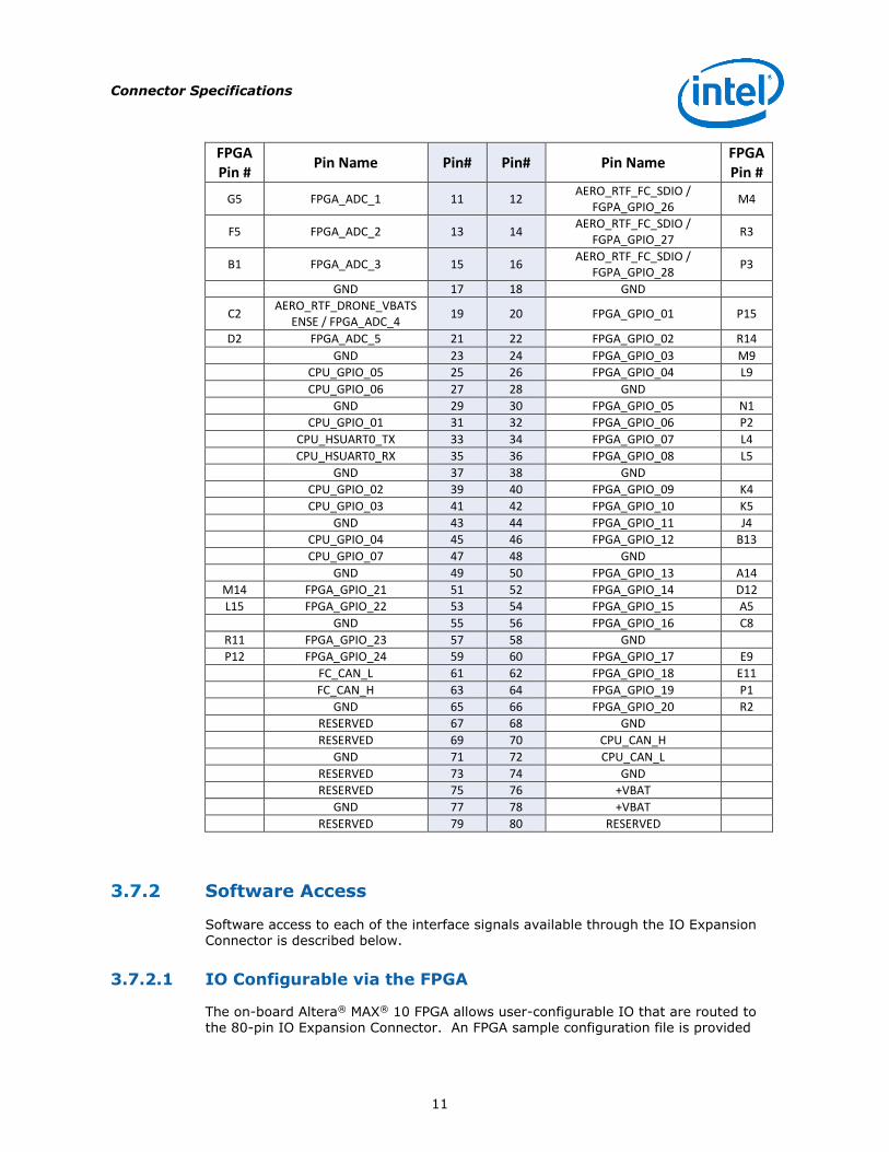
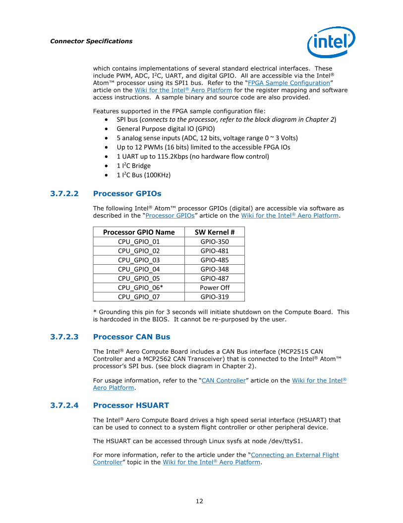
3.7.1 Connector Pin Definition
The Intel® Aero Compute Board has a configurable 80-pin IO Expansion Connector. In addition to power and ground pins, this connector provides access to the processor GPIOs and processor HSUART. The on-board Altera® MAX® 10 FPGA provides an additional 24 FPGA GPIOs and 5 FPGA analog inputs (ADC). The FPGA is accessible using the processor SPI1 interface (chip select 1).
A dedicated CAN bus is also available and accessible using the same SPI1 bus (chip select 0).
The IO Expansion Connector pin definition and pin mapping to the FPGA are captured in the table below.
Figure 7. IO Expansion Connector Pin Orientation
FPGA Pin #
Pin Name Pin# Pin# Pin Name FPGA Pin #
+3.3V 1 2 +3.3V
+3.3V 3 4 +3.3V
GND 5 6 GND
GND 7 8 GND
GND 9 10 AERO_RTF_FC_SDIO /
FGPA_GPIO_25 M5
Pin 1indicator
Connector Specifications
11
FPGA Pin #
Pin Name Pin# Pin# Pin Name FPGA Pin #
G5 FPGA_ADC_1 11 12 AERO_RTF_FC_SDIO /
FGPA_GPIO_26 M4
F5 FPGA_ADC_2 13 14 AERO_RTF_FC_SDIO /
FGPA_GPIO_27 R3
B1 FPGA_ADC_3 15 16 AERO_RTF_FC_SDIO /
FGPA_GPIO_28 P3
GND 17 18 GND
C2 AERO_RTF_DRONE_VBATS
ENSE / FPGA_ADC_4 19 20 FPGA_GPIO_01 P15
D2 FPGA_ADC_5 21 22 FPGA_GPIO_02 R14
GND 23 24 FPGA_GPIO_03 M9
CPU_GPIO_05 25 26 FPGA_GPIO_04 L9
CPU_GPIO_06 27 28 GND
GND 29 30 FPGA_GPIO_05 N1
CPU_GPIO_01 31 32 FPGA_GPIO_06 P2
CPU_HSUART0_TX 33 34 FPGA_GPIO_07 L4
CPU_HSUART0_RX 35 36 FPGA_GPIO_08 L5
GND 37 38 GND
CPU_GPIO_02 39 40 FPGA_GPIO_09 K4
CPU_GPIO_03 41 42 FPGA_GPIO_10 K5
GND 43 44 FPGA_GPIO_11 J4
CPU_GPIO_04 45 46 FPGA_GPIO_12 B13
CPU_GPIO_07 47 48 GND
GND 49 50 FPGA_GPIO_13 A14
M14 FPGA_GPIO_21 51 52 FPGA_GPIO_14 D12
L15 FPGA_GPIO_22 53 54 FPGA_GPIO_15 A5
GND 55 56 FPGA_GPIO_16 C8
R11 FPGA_GPIO_23 57 58 GND
P12 FPGA_GPIO_24 59 60 FPGA_GPIO_17 E9
FC_CAN_L 61 62 FPGA_GPIO_18 E11
FC_CAN_H 63 64 FPGA_GPIO_19 P1
GND 65 66 FPGA_GPIO_20 R2
RESERVED 67 68 GND
RESERVED 69 70 CPU_CAN_H
GND 71 72 CPU_CAN_L
RESERVED 73 74 GND
RESERVED 75 76 +VBAT
GND 77 78 +VBAT
RESERVED 79 80 RESERVED
3.7.2 Software Access
Software access to each of the interface signals available through the IO Expansion Connector is described below.
3.7.2.1 IO Configurable via the FPGA
The on-board Altera® MAX® 10 FPGA allows user-configurable IO that are routed to the 80-pin IO Expansion Connector. An FPGA sample configuration file is provided
Connector Specifications
12
which contains implementations of several standard electrical interfaces. These include PWM, ADC, I2C, UART, and digital GPIO. All are accessible via the Intel® Atom™ processor using its SPI1 bus. Refer to the “FPGA Sample Configuration” article on the Wiki for the Intel® Aero Platform for the register mapping and software access instructions. A sample binary and source code are also provided.
Features supported in the FPGA sample configuration file:
SPI bus (connects to the processor, refer to the block diagram in Chapter 2)
General Purpose digital IO (GPIO)
5 analog sense inputs (ADC, 12 bits, voltage range 0 ~ 3 Volts)
Up to 12 PWMs (16 bits) limited to the accessible FPGA IOs
1 UART up to 115.2Kbps (no hardware flow control)
1 I2C Bridge
1 I2C Bus (100KHz)
3.7.2.2 Processor GPIOs
The following Intel® Atom™ processor GPIOs (digital) are accessible via software as described in the “Processor GPIOs” article on the Wiki for the Intel® Aero Platform.
Processor GPIO Name SW Kernel # CPU_GPIO_01 GPIO-350
CPU_GPIO_02 GPIO-481
CPU_GPIO_03 GPIO-485
CPU_GPIO_04 GPIO-348
CPU_GPIO_05 GPIO-487
CPU_GPIO_06* Power Off
CPU_GPIO_07 GPIO-319
* Grounding this pin for 3 seconds will initiate shutdown on the Compute Board. This
is hardcoded in the BIOS. It cannot be re-purposed by the user.
3.7.2.3 Processor CAN Bus
The Intel® Aero Compute Board includes a CAN Bus interface (MCP2515 CAN
Controller and a MCP2562 CAN Transceiver) that is connected to the Intel® Atom™ processor’s SPI bus. (see block diagram in Chapter 2). For usage information, refer to the “CAN Controller” article on the Wiki for the Intel® Aero Platform.
3.7.2.4 Processor HSUART
The Intel® Aero Compute Board drives a high speed serial interface (HSUART) that can be used to connect to a system flight controller or other peripheral device.
The HSUART can be accessed through Linux sysfs at node /dev/ttyS1.
For more information, refer to the article under the “Connecting an External Flight Controller” topic in the Wiki for the Intel® Aero Platform.
Connector Specifications
13
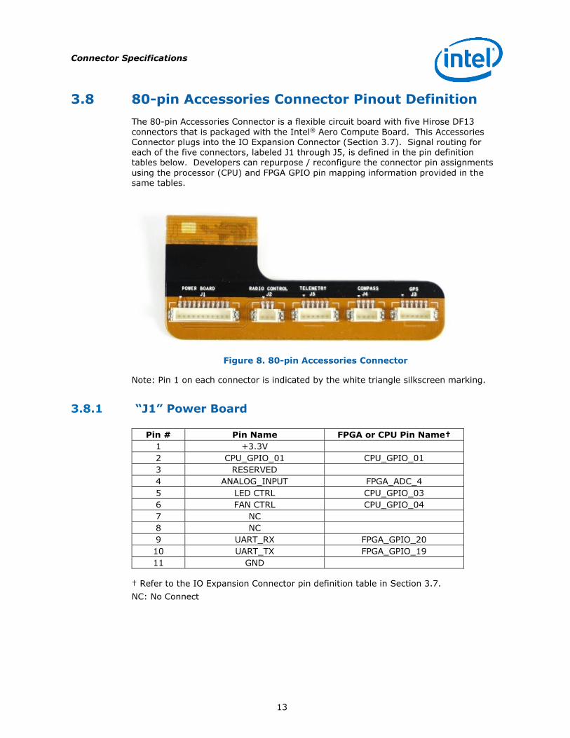
3.8 80-pin Accessories Connector Pinout Definition
The 80-pin Accessories Connector is a flexible circuit board with five Hirose DF13
connectors that is packaged with the Intel® Aero Compute Board. This Accessories Connector plugs into the IO Expansion Connector (Section 3.7). Signal routing for each of the five connectors, labeled J1 through J5, is defined in the pin definition tables below. Developers can repurpose / reconfigure the connector pin assignments
using the processor (CPU) and FPGA GPIO pin mapping information provided in the same tables.
Figure 8. 80-pin Accessories Connector
Note: Pin 1 on each connector is indicated by the white triangle silkscreen marking.
3.8.1 “J1” Power Board
Pin # Pin Name FPGA or CPU Pin Name†
1 +3.3V
2 CPU_GPIO_01 CPU_GPIO_01
3 RESERVED
4 ANALOG_INPUT FPGA_ADC_4
5 LED CTRL CPU_GPIO_03
6 FAN CTRL CPU_GPIO_04
7 NC
8 NC
9 UART_RX FPGA_GPIO_20
10 UART_TX FPGA_GPIO_19
11 GND
† Refer to the IO Expansion Connector pin definition table in Section 3.7.
NC: No Connect
Connector Specifications
14
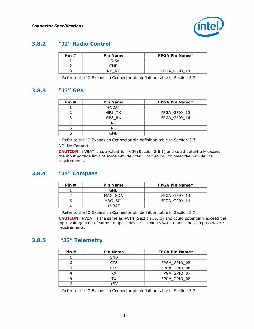
3.8.2 “J2” Radio Control
Pin # Pin Name FPGA Pin Name†
1 +3.3V
2 GND
3 RC_RX FPGA_GPIO_18
† Refer to the IO Expansion Connector pin definition table in Section 3.7.
3.8.3 “J3” GPS
Pin # Pin Name FPGA Pin Name†
1 +VBAT
2 GPS_TX FPGA_GPIO_15
3 GPS_RX FPGA_GPIO_16
4 NC
5 NC
6 GND
† Refer to the IO Expansion Connector pin definition table in Section 3.7.
NC: No Connect
CAUTION: +VBAT is equivalent to +VIN (Section 3.6.1) and could potentially exceed the input voltage limit of some GPS devices. Limit +VBAT to meet the GPS device requirements.
3.8.4 “J4” Compass
Pin # Pin Name FPGA Pin Name†
1 GND
2 MAG_SDA FPGA_GPIO_13
3 MAG_SCL FPGA_GPIO_14
4 +VBAT
† Refer to the IO Expansion Connector pin definition table in Section 3.7.
CAUTION: +VBAT is the same as +VIN (Section 3.6.1) and could potentially exceed the input voltage limit of some Compass devices. Limit +VBAT to meet the Compass device requirements.
3.8.5 “J5” Telemetry
Pin # Pin Name FPGA Pin Name†
1 GND
2 CTS FPGA_GPIO_05
3 RTS FPGA_GPIO_06
4 RX FPGA_GPIO_07
5 TX FPGA_GPIO_08
6 +5V
† Refer to the IO Expansion Connector pin definition table in Section 3.7.
On-Board Sensors
15
4 On-Board Sensors
The Intel® Aero Compute Board is designed with a 6 Degree of Freedom IMU (BMI160), a magnetometer (BMM150), and an altimeter (MS5611). The sensors are connected to the processor SPI bus and I2C bus.
Full details how to access each sensor can be found in the article “Onboard Sensors” on the Wiki for the Intel® Aero Platform.
LED Definition and Usage
16
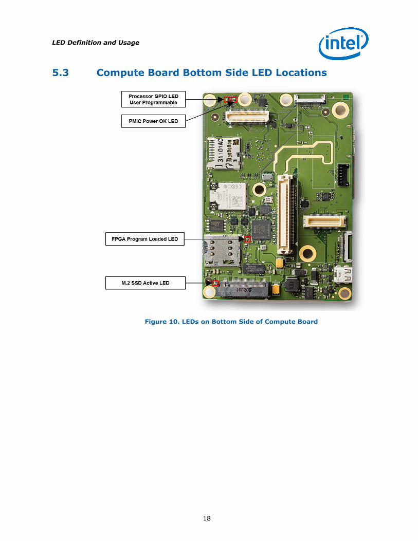
5 LED Definition and Usage
5.1 Compute Board LEDs
The Intel® Aero Compute Board has a total of 8 LEDs. Four are located on the top
side of the board. The other Four LEDs are located on the bottom side. Refer to Figure 9 and Figure 10
The table below describes each LED and its function. Two of the LEDs can be programmed via software as described in the “LEDs” article on the Wiki for the Intel® Aero Platform.
LED Color LED “ON” Function Software controlled
GPIO?
Green FPGA Program Loaded LED No
Green PMIC Power OK No
Green Processor Power On LED No
Green M.2 SSD Active LED No
Green M.2 Power On LED No
Green Flight Controller Connected LED No
Orange User Programmable Yes
Processor GPIO # 507
Tricolor
Red Yes
Processor GPIO # 437
Green Yes
Processor GPIO # 341
Blue Yes
Processor ISH GPIO # 347
Note that the “Flight Controller Connected LED” is used only with the Intel® Aero Flight Controller which is assembled with the Intel® Aero Ready to Fly Drone.
LED Definition and Usage
17
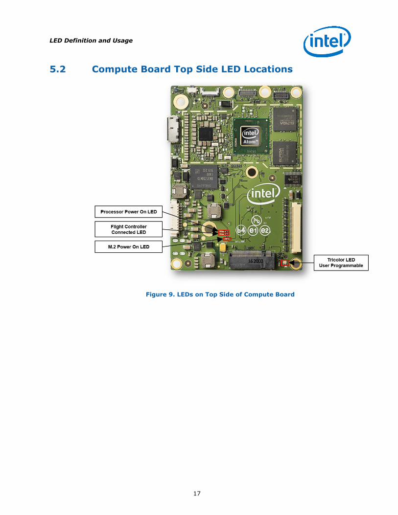
5.2 Compute Board Top Side LED Locations
Figure 9. LEDs on Top Side of Compute Board
LED Definition and Usage
18
5.3 Compute Board Bottom Side LED Locations
Figure 10. LEDs on Bottom Side of Compute Board
Intel® Aero Flight Controller
19
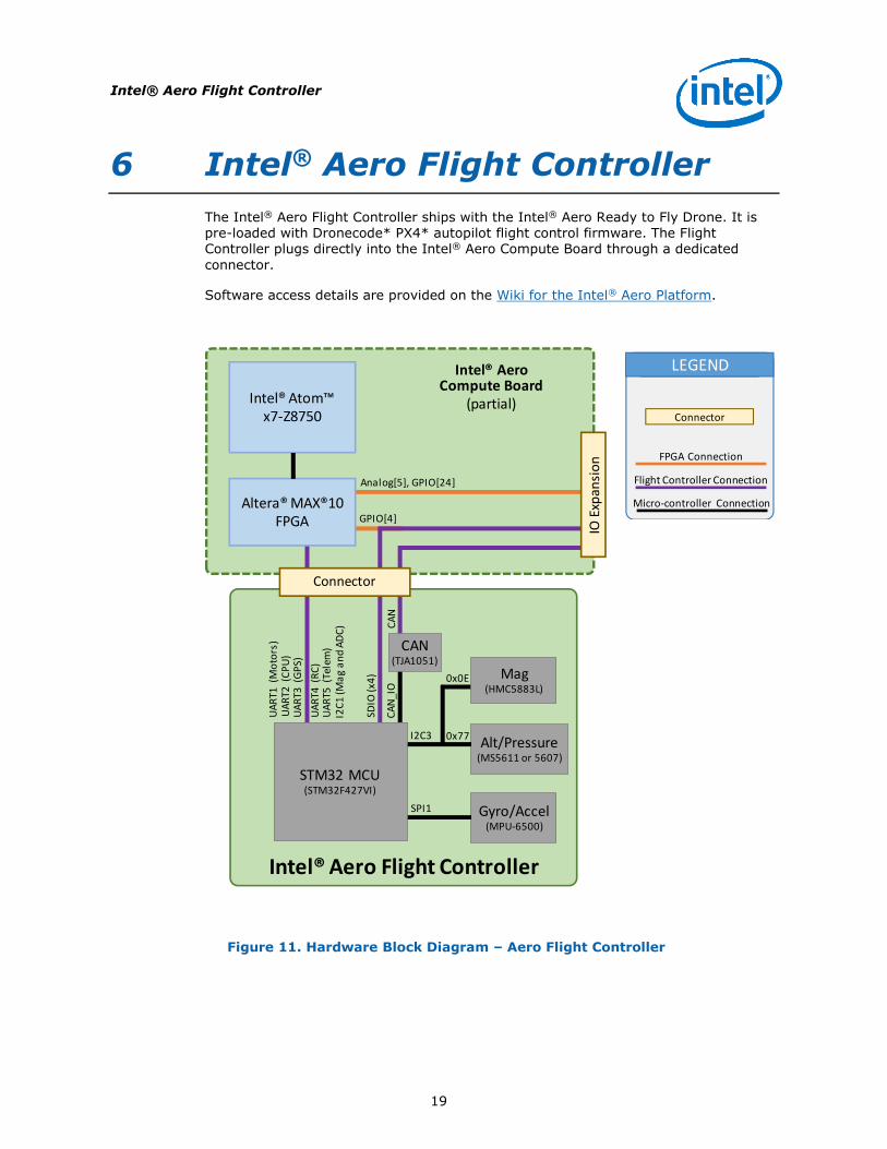
6 Intel® Aero Flight Controller
The Intel® Aero Flight Controller ships with the Intel® Aero Ready to Fly Drone. It is pre-loaded with Dronecode* PX4* autopilot flight control firmware. The Flight Controller plugs directly into the Intel® Aero Compute Board through a dedicated
connector.
Software access details are provided on the Wiki for the Intel® Aero Platform.
Figure 11. Hardware Block Diagram – Aero Flight Controller
UA
RT2
(C
PU
)
Gyro/Accel(MPU-6500)
SPI1
Alt/Pressure(MS5611 or 5607)
Mag(HMC5883L)
0x77
0x0E
I2C3
UA
RT1
(M
oto
rs)
UA
RT3
(G
PS)
I2C
1 (M
ag
an
d A
DC
)
UA
RT4
(R
C)
UA
RT5
(Te
lem
)
SDIO
(x4
)
Intel® Aero Flight Controller
Analog[5], GPIO[24]
Intel® Aero Compute Board
(partial)
GPIO[4]Altera® MAX®10
FPGA
Intel® Atom™x7-Z8750
CA
N_I
O
ConnectorIO
Exp
ansi
on
STM32 MCU(STM32F427VI)
CAN(TJA1051)
CA
N
Connector
FPGA Connection
Flight Controller Connection
LEGEND
Micro-controller Connection