Embed Size (px)
Citation preview

Japan Advanced Institute of Science and Technology
JAIST Repositoryhttps://dspace.jaist.ac.jp/
Title
Integration of a Low-Voltage Organic Field-Effect
Transistor and a Sensing Capacitor for a
Pressure-Sensing Device
Author(s) Sakai, Heisuke; Tsuji, Yushi; Murata, Hideyuki
CitationIEICE Transactions on Electronics, E100-C(2):
126-129
Issue Date 2017-02-01
Type Journal Article
Text version publisher
URL http://hdl.handle.net/10119/14716
Rights
Copyright (C)2017 IEICE. Heisuke Sakai, Yushi
Tsuji, Hideyuki Murata, IEICE Transactions on
Electronics, E100-C(2), 2017, 126-129.
http://www.ieice.org/jpn/trans_online/
Description
126IEICE TRANS. ELECTRON., VOL.E100–C, NO.2 FEBRUARY 2017
BRIEF PAPER Special Section on Recent Progress in Organic Molecular Electronics
Integration of a Low-Voltage Organic Field-Effect Transistor and aSensing Capacitor for a Pressure-Sensing Device
Heisuke SAKAI†, Member, Yushi TSUJI†, and Hideyuki MURATA†a), Nonmembers
SUMMARY We integrate a pressure sensing capacitor and a low oper-ation voltage OFET to develop a pressure sensor. The OFET was used as areadout device and an external pressure was loaded on the sensing capaci-tor. The OFET operates at less than 5 V and the change in the drain currentin response to the pressure load (100 kPa) is two orders of magnitude.key words: low-voltage operation, pressure sensor, organic field-effecttransistor, ferroelectric polymer
1. Introduction
Recently, an organic pressure sensing devices have at-tracted much attention regarding the development of arti-ficial skins, the health monitoring devices and the pressuresensing sheets, and several sensing devices such as capaci-tive sensors, piezoelectric sensors and transistor sensor havebeen reported [1]–[3]. Research-based development oftenfocuses on the fabrication of the pressure sensors on flexibleplastic substrates because devices flexibility is an essentialfactor for the artificial skin [4]. On the other hand, the reduc-tion of the operation voltage and sensitivity improvementare necessary for practical applications. Pressure sensingwith an organic field-effect transistor (OFET) as a readoutdevice of the pressure load is promising owing to its advan-tages such as high sensitivity to the pressure load and lowersusceptibility to electrical crosstalk. For example, a pressuresensor matrix of OFETs has been reported. The 32 × 32 ar-ray of sensor cells is fabricated on a plastic substrate, wherea pressure image of a kiss mark on the sheet was obtainedwith a −20 V operating bias [5]. Y. Zang et al. reported anOFET with a suspended gate that exhibited ultra-sensitivity(192 kPa−1) for the pressure detection, where the change inthe drain current (ID) in response to the pressure load (5 kPa)was more than three orders of magnitude with a −60 V op-erating bias [6]. Further reduction of operating voltage ofthe pressure sensing OFETs is necessary for practical appli-cations. Thus, the development of a pressure sensing OFETthat satisfies both low-voltage operation and high sensitivityis essential. A pressure-modulated OFET with an ultra-thin,hybrid organic/inorganic gate dielectric layer exhibits lowoperation voltage (2 V) [7]. Although the device operateswith a low-voltage, the change in the ID in response to thepressure load is limited to c.a. 5% of the initial value. In
Manuscript received May 31, 2016.Manuscript revised July 29, 2016.†The authors are with Japan Advanced Institute of Science and
Technology, Nomi-shi, 923–1211 Japan.a) E-mail: [email protected]
DOI: 10.1587/transele.E100.C.126
this study, we demonstrate an excellent pressure sensor witha low operation voltage and high pressure response by in-tegrating a sensing capacitor using a piezoelectric polymerfilm and a low-voltage OFET as a readout device. Our pres-sure sensor operates at less than −6 V and the change in theID in response to the pressure load (100 kPa) is two ordersof magnitude, where ID of the OFET changes from 120 nAto 5 nA.
2. Experimental
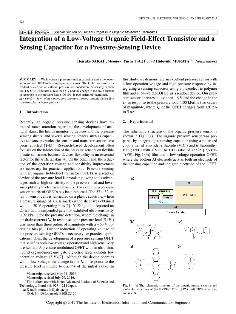
The schematic structure of the organic pressure sensor isshown in Fig. 1 (a). The organic pressure sensor was pre-pared by integrating a sensing capacitor using a polarizedcopolymer of vinylidene fluoride (VDF) and trifluoroethy-lene (TrFE) with a VDF to TrFE ratio of 75 : 25 [P(VDF-TrFE), Fig. 1 (b)] film and a low-voltage operation OFET,where the bottom Al electrode acts as both an electrode ofthe sensing capacitor and the gate electrode of the OFET.
Fig. 1 (a) The schematic structure of the organic pressure sensor andmolecular structures of (b) P(VDF-TrFE), (c) PVC, (d) TIPS-pentacene,and (e) PS.
Copyright c© 2017 The Institute of Electronics, Information and Communication Engineers

BRIEF PAPER127
The Al bottom electrode (60 nm) was thermally evapo-rated onto a glass substrate. Prior to the fabrication of theOFET, the sensing capacitor was fabricated. As the pressuresensing material of the sensing capacitor, the P(VDF-TrFE)piezoelectric layer (8 µm) was blade coated on the Al bot-tom electrode. The Al top electrode (50 nm) was evaporatedonto the P(VDF-TrFE) piezoelectric layer, followed by thepolarization of the layer by a contact poling method. A pol-ing voltage of 1 kV was applied to the Al top electrode andAl bottom electrode was grounded. As the gate dielectriclayer of the OFET, poly(vinyl cinamate) [PVC, Fig. 1 (c)](220 nm) was spin coated and cross linked by UV irradia-tion. Ag source/drain electrodes (50 nm) were evaporatedwith a shadow mask. The channel width (W) and channellength (L) of the electrodes were 2 mm and 50 µm, respec-tively. The electrodes were modified by immersion in a so-lution of pentafluorothiophenol in ethanol at a concentra-tion of 5 × 10⁻³ mol/L. The semiconducting layer (100 nm)was then spin coated from a mixed solution consisting of3 : 1 by weight blend of 6,13-bis(triisopropyl-silylethynyl)pentacene [TIPS-Pentacene, Fig. 1 (d)] and Polystyrene [PS,Fig. 1 (e)] at 0.01 g/mL concentration of solids. The pres-sure response of the device was measured as the change inthe drain current (ID) of the OFET at a certain drain voltage(VD) by applying a pressure (100 kPa) to the P(VDF-TrFE)sensing capacitor. The pressure was loaded with a home-made pressure load system. Electrical measurements of theOFETs were carried out at room temperature (23◦C) usinga Keithley 4200 semiconductor characterization system in adry nitrogen atmosphere.
The surface morphology of the PVC dielectriclayer was measured with a HITACHI High-Tech ScienceAFM5000II, and a polarized optical microscope imageof the active layer was obtained with a Nikon ECLIPSEE400POL.
For the Fourier-transform infrared (FT-IR) measure-ment of polarized P(VDF-TrFE) film, the film was preparedon an Si substrate. The conditions to prepare the film andto polarize the P(VDF-TrFE) film were the same as thoseused to prepare the sensing capacitor. The FT-IR absorptionspectra were measured with a Thermo Nicolet 6700 FT-IRspectrometer. The resolution of the spectra was 4 cm−1, andthe number of scans collected was 128.
3. Results and Discussion
Figure 2 (a) shows an atomic force microscope (AFM) im-age of the PVC gate dielectric surface. The film was foundto have a very smooth and pinhole-free surface, with a root-mean square roughness of 0.20 nm within a 5 × 5 µm2 scanscale, which is much smoother than the value (0.67 nm) forthe of PVC film previously reported [8]. Figure 2 (b) showsa polarized microscope image of the TIPS-pentacene/PS ac-tive layer. As can be seen, the high crystallinity of the ac-tive layer is confirmed. These results lead us to expect thelow-voltage operation of the OFET as gate dielectric surfacesmoothness and high crystallinity of the active layer are key
Fig. 2 (a) AFM image of the PVC surface. (b) Polarization microscopeimage of TIPS-pentacene and PS active layer.
Fig. 3 (a) The output characteristics of the OFET (b) The transfer char-acteristics of the OFET.
factors for the low-voltage OFET operation [9].Figures 3 (a) and 3 (b) show the output characteristics
and the transfer characteristics of the OFET. In the outputcharacteristics, the gate voltage (VG) was swept from 0 to−5 V with a step voltage of 1 V. A clear increase in ID as afunction of VG was observed despite the low VG application.In addition, ID was tended to saturate below VG of −5 Vas shown in Fig. 2 (b), where the ON/OFF ratio, mobility,threshold voltage (Vth) and threshold swing were 1.3 × 105,0.29 cm2/Vs, −1.25 V and 0.26 V/dec, respectively. Fromthese results, we confirmed the low operation voltage of theOFET.
The pressure-sensing device was fabricated by integrat-ing the low-voltage OFET and the sensing capacitor. Prior tothe integration, the P(VDF-TrFE) film in the sensing capaci-tor is polarized by means of a contact poling method. Whilea poling voltage of 1 kV was applied to the Al top electrode,the Al bottom electrode was grounded. Thus, the directionof the polarization in the P(VDF-TrFE) film is from the bot-tom to the top. To confirm the electric field polarization inthe P(VDF-TrFE) film induced by the change in the orien-tation of the P(VDF-TrFE) polymer chain, an FT-IR mea-surement of the film was conducted, where the orientationchange of polar functional groups in the polymer chain canbe observed as a change in the corresponding bands of theFT-IR spectra [10], [11]. In order to clarify the change inthe spectra of the P(VDF-TrFE) after poling treatment, thedifference spectrum was calculated by subtracting the spec-trum of the polarized film from that of the pristine film. Aclear difference in the bands before and after poling treat-

128IEICE TRANS. ELECTRON., VOL.E100–C, NO.2 FEBRUARY 2017
Fig. 4 (a) The ID of the OFET integrated with the sensing capacitor us-ing the pristine P(VDF-TrFE) film and the polarized P(VDF-TrFE) filmat VD = −6 V. (b) The the ID response of the OFET integrated with thesensing capacitor using the pristine P(VDF-TrFE) film and the polarizedP(VDF-TrFE) film at VD = −6 V.
ment was observed, which is consistent with the previousreports [10], [11]. A detailed analysis on the FT-IR spec-tra will be reported elsewhere. The change in the bandsindicates that the polar C-F bonds in the film are orientedalong the direction of the external electric field during thepoling treatment. In addition, the orientation of the bondis maintained after removal of the electric field. Thus, weconcluded that the P(VDF-TrFE) film was successfully po-larized by the contact poling treatment.
Figure 4 (a) shows the ID at VD = −6 V for the OFET.The ID increased from 285 pA to 120 nA by integratingthe sensing capacitor with the polarized P(VDF-TrFE). Thissuggests that the polarization in the P(VDF-TrFE) film in-duced the charge accumuration in the OFET channel. Asthe sensing capacitor and the OFET are integrated via thebottom electrode, the bottom electrode serve as the gateelectrode of the OFET. Thus, the polarization of the film inthe sensing capacitor applies an electric potential to the ac-tive layer of the OFET and consequently induces a changein the ID. This is consistent with the changes observed inthe device with similar structure [7], [12]. The change inthe ID induced by the polarization is produce shifts of thetransfer curve and the Vth [13], [14]. In our device, how-ever, the measurement of the transfer curve after integrationwas not succesful owing to electrical noise in the measure-ment, which was caused by the electrostatic charges in thepolarized P(VDF-TrFE) layer. As can be seen in Fig. 4 (a),
the typical ID of our typical OFETs exceeded 100 nA afterintegration with the sensing capacitor, despite the measure-ment having been carried out without VG application to theOFET. The value of ID is consistent with that at approxi-mately VG = −3 V in Fig. 3 (a). Thus, we assume the effectof the polarization on the Vth shift would be c.a. 3 V inour integrated device. Figure 4 (b) shows the ID responseof the OFET integrated with the sensing capacitor using thepristine P(VDF-TrFE) film and the polarized P(VDF-TrFE)film. In the case of the sensor device with the polarizedP(VDF-TrFE) film, ID decreased from 120 nA to 5 nA byapplying a pressure of 100 kPa. The variation of ID was ap-proximatly 16 times larger than that of a reported pressuresensor with a similar structure [1]. In addition, the changein the ID caused by the pressure load is more than 95% ofthe initial value, which is significantly improved over thechange (5%) for a pressure sensor using the low-voltageoperation OFET [7]. After the release of the pressure, ID
slowly returned to the initial value, with a slow deformationof the P(VDF-TrFE) layer to its initial form. In contrast, inthe case of the sensor device with the non-polarized (pris-tine) P(VDF-TrFE) film, no ID difference against the pres-sure load was observed. This indicates that the polarizationin the sensing capacitor is imperative for our sensor device.Furthermore, when the OFET of the sensor using the polar-ized P(VDF-TrFE) film was replaced by an OFET requir-ing high-voltage operation (60 V), the pressure response ofthe sensor was approximatly 10 times smaller than that ofour device (data not shown). Thus, we concluded that theintegration of the pressure sensing capacitors and the lowoperation voltage OFETs is critical to the development ofhigh-performance pressure sensors. In particular, by usinga low-voltage OFET with a sensing capacitor, we have suc-ceeded in demonstratting a pressure sensing OFET that sat-isfies both low-voltage operation and high sensitivity.
4. Conclusion
In conclusion, we successfully achieved the pressure re-sponse at low operation voltage in our organic pressure sen-sor. The organic pressure sensor was prepared by integratingthe sensing capacitor and the low-voltage operation OFET.The OFET was employed as the readout device of the pres-sure load and was operated below −6V. The sensing capaci-tor was prepared by using a polarized P(VDF-TrFE) film. ID
was changed from 120 nA to 5 nA by applying the pressure.The variation of ID is approximately 10 times larger thanthat detected by a pressure sensor with a similar structure.We believe that the integration of the low-voltage OFETsand the sensing capasitors will be a one of the key technolo-gies to develop the pressure sensor sheets.
Acknowledgments
Part of this work was supported by JSPS KAKENHI GrantNumber 16K21061.
BRIEF PAPER129
References
[1] I. Graz, M. Kaltenbrunner, C. Keplinger, R. Schwodiauer, S. Bauer,S.P. Lacour, and S. Wagner, “Flexible ferroelectret field-effect tran-sistor for large-area sensor skins and microphones,” Appl. Phys.Lett., vol.89, no.7, pp.073501–073503, 2006.
[2] M.L. Hammock, A. Chortos, B.C.-K. Tee, J.B.-H. Tok, and Z.Bao, “25th Anniversary Article: The Evolution of Electronic Skin(E-Skin): A Brief History, Design Considerations, and RecentProgress,” Adv. Mater., vol.25, no.42, pp.5997–6038, 2013.
[3] Y. Watanabe, S. Uemura, and S. Hoshino, “Printed pressure sensorarray sheets fabricated using poly(amino acid)-based piezoelectricelements,” Jpn. J. Appl. Phys., vol.53, no.5S3, p.05HB15, 2014.
[4] H. Mei, R. Wang, Z. wang, J. Feng, Y. Xia, and T. Zhang, “A flex-ible pressure-sensitive array based on soft substrate,” Sensors andActuators A: Physical, vol.222, pp.80–86, 2015.
[5] T. Someya, T. Sekitani, S. Iba, Y. Kato, H. Kawaguchi, and T.Sakurai, “A large-area, flexible pressure sensor matrix with organicfield-effect transistors for artificial skin applications,” Proc. Natl.Acad. Sci. U.S.A., vol.101, no.27, pp.9966–9970, 2004.
[6] Y. Zang, F. Zhang, D. Huang, X. Gao, C.-A. Di, and D. Zhu, “Flex-ible suspended gate organic thin-film transistors for ultra-sensitivepressure detection,” Nat Commun, vol.6, 2015.
[7] S. Lai, P. Cosseddu, A. Bonfiglio, and M. Barbaro, “Ultralow Volt-age Pressure Sensors Based on Organic FETs and Compressible Ca-pacitors,” Electron Device Letters, IEEE, vol.34, no.6, pp.801–803,2013.
[8] J. Jang, S.H. Kim, S. Nam, D.S. Chung, C. Yang, W.M. Yun, C.E.Park, and J.B. Koo, “Hysteresis-free organic field-effect transistorsand inverters using photocrosslinkable poly(vinyl cinnamate) as agate dielectric,” Appl. Phys. Lett., vol.92, no.14, p.143306, 2008.
[9] L. Feng, W. Tang, X. Xu, Q. Cui, and X. Guo, “Ultralow-Volt-age Solution-Processed Organic Transistors With Small Gate Di-electric Capacitance,” Electron Device Letters, IEEE, vol.34, no.1,pp.129–131, 2013.
[10] H. Isoda and Y. Furukawa, “Effect of electric field on the infraredspectrum of a ferroelectric poly(vinylidene fluoride-co-hexafluoro-propylene) film,” Vib. Spectrosc, vol.78, pp.12–16, 2015.
[11] X. Ma, J. Liu, C. Ni, D.C. Martin, D.B. Chase, and J.F. Rabolt,“Molecular Orientation in Electrospun Poly(vinylidene fluoride)Fibers,” ACS Macro Letters, vol.1, no.3, pp.428–431, 2012.
[12] M. Zirkl, A. Haase, A. Fian, H. Schon, C. Sommer, G. Jakopic, G.Leising, B. Stadlober, I. Graz, N. Gaar, R. Schwodiauer, S. Bauer-Gogonea, and S. Bauer, “Low-Voltage Organic Thin-Film Tran-sistors with High-k Nanocomposite Gate Dielectrics for FlexibleElectronics and Optothermal Sensors,” Adv. Mater., vol.19, no.17,pp.2241–2245, 2007.
[13] H. Sakai, K. Konno, and H. Murata, “Control of threshold voltageof organic field-effect transistors by space charge polarization,” ThinSolid Films, vol.518, no.2, pp.510–513, 2009.
[14] H. Sakai, K. Konno, and H. Murata, “Tuning of threshold voltage oforganic field-effect transistors by space charge polarization,” Appl.Phys. Lett., vol.94, no.7, p.073304, 2009.